Note: Descriptions are shown in the official language in which they were submitted.
84424200
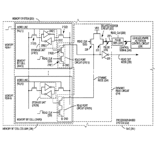
LEAKAGE-AWARE ACTIVATION CONTROL OF A DELAYED KEEPER CIRCUIT
FOR A DYNAMIC READ OPERATION IN A MEMORY BIT CELL
PRIORITY APPLICATION
[0001]
The present application claims priority to U.S. Patent Application Serial No.
15/085,187, filed on March 30, 2016, and entitled "LEAKAGE-AWARE ACTIVATION
CONTROL OF A DELAYED KEEPER CIRCUIT FOR A DYNAMIC READ OPERATION IN A
MEMORY BIT CELL".
BACKGROUND
I. Field of the Disclosure
[0002]
The technology of the disclosure relates generally to memory systems employing
memory bit cells for storing data, and more particularly to dynamic read
circuits for performing
dynamic read operations in a memory bit cell.
Background
[0003]
Processor-based systems that include a central processing unit (CPU) or other
processors utilize memory of varying types for system operations. This memory
may be used as
system memory for data storage. This memory may also be used to store program
code or
instructions to be executed by a CPU or processor.
[0004]
For example, Figure 1 illustrates a memory system 100 that can be provided in
a
processor-based system. The memory system 100 in this particular example
employs memory bit
cells 102(1)-102(N) for storing data, as shown in Figure 1. Each memory bit
cell 102 is capable of
storing a single bit of information. In Figure 1, a single memory bit cell
column 104 is shown that
contains a plurality of memory bit cells 102(1)-102(N), wherein 'N' can be any
number of rows of
memory bit cells desired. However, note that multiple memory bit cell columns
104 may be
provided in the memory system 100 to provide a data array of the memory bit
cells 102(1)-102(N).
In this example, the memory bit cells 102(1)-102(N) are provided in the form
of eight (8) transistor
(T) (8-T) complement memory bit cells. Using memory bit cell 102(1) as a
reference example, each
memory bit cell 102(1)-102(N) includes two (2) cross-
1
Date Recue/Date Received 2022-01-27
CA 03016028 2018-08-28
WO 2017/172230
PCMJS2017/020351
coupled inverters 106(1), 106(2) (i.e., four (4) transistors) and two (2)
access transistors
108(1), 108(2) configured to be activated by a row word line VVL(1) for the
accessed
memory row 1 of the memory bit cell 102(1) for performing write operations, as
is well
known. Two (2) additional transistors, a pull-down NFET 110(1) and a read port
NFET
110(2), as provided for the memory bit cell 102(1) as part of a dynamic read
circuit 112
for performing read operations in the memory bit cell 102(1). The dynamic read
circuit
112 performs read operations for each of the memory bit cells 102(1)-102(N)
for the
memory bit cell column 104. The assertion of a particular word line WL(1)-
WL(N) for
a given respective memory row 1-N controls which memory bit cell 102(1)-102(N)
is
read by the dynamic read circuit 112 during a read operation. Providing the
additional
pull-down NFET 110(1) and read port NFET 110(2) in the dynamic read circuit
112
decouples write performance of the memory bit cell 102(1) from read
performance of
the memory bit cell 102(1).
[0005] During a pre-
charge phase of the memory bit cell 102(1), a charge P-type
Field-Effect Transistor (PFET) 116 is activated in response to a read clock
signal
(read_clk) 118 being a low logic level indicating that a read operation is not
active.
This causes a dynamic node 120 in the dynamic read circuit 112 to be pre-
charged to
voltage Vdd. Then, during an evaluation phase in response to the read clock
signal
(read_clk) 118 being a logic high level indicating a read operation, the PPET
116 is
turned off and the pull-down NFET 110(1) is activated to be coupled to ground
(GND).
If the charge on a complement node 122C in the selected memory bit cell 102(1)-
102(N) is a logical '1' (i.e., voltage Vdd) during a read operation, the pull-
down NFET
110(1) is activated to pull the dynamic node 120 down to ground (GND). Pulling
the
dynamic node 120 to ground (GND) will cause a logical '1' to generate on a
read out
node 124 by an inverter 126. However, a keeper circuit 128 is initially
activated by the
complement node 122C having a logical '1' state during the read operation,
which
causes the inverter 126 to generate a logical '0' on the read out node 124 and
keep the
keeper circuit 128 activated thereby pulling the dynamic node 120 up to
voltage Vdd in
contention with the pull-down NFET 110(1).
2
CA 03016028 2018-08-28
WO 2017/172230
PCT/US2017/020351
SUMMARY OF THE DISCLOSURE
[0006] Aspects of
the disclosure involve leakage-aware activation control of a
delayed keeper circuit for a dynamic read operation in a memory bit cell. In
this regard,
in one aspect, a leakage-aware activation control circuit is provided for a
dynamic read
circuit configured to perform read operations on a memory bit cell. The
dynamic read
circuit includes a delayed keeper circuit configured to keep a read out value
from the
selected memory bit cell asserted on a dynamic node in the dynamic read
circuit during
an evaluation phase of a dynamic read operation. To prevent or mitigate
contention
between the delayed keeper circuit and a read port circuit in the dynamic read
circuit
pulling the dynamic node to opposite voltage levels when a read operation is
initiated,
the delayed keeper circuit is selectively deactivated during the evaluation
phase.
However, because factors such as process variation and technology node scaling
can
affect leakage current of transistors in the delayed keeper circuit and the
read port
circuit, and thus their relative transistor strengths, aspects disclosed
herein include the
leakage-aware activation control circuit for controlling activation timing of
the delayed
keeper circuit. The leakage-aware activation control circuit is configured to
adaptively
control the activation timing of the delayed keeper circuit based on a
comparison of N-
type Field-Effect Transistor (NFET) leakage current to P-type FET (PELT)
leakage
current. In this manner, if the relative strengths of the NFETs and PFETs in
the delayed
keeper circuit and read port circuit of the dynamic read circuit vary from
design time
assumptions, the leakage-aware activation control circuit can adaptively
adjust the
activation timing of the delayed keeper circuit based on the actual relative
strengths of
the NFETs and PFETs to avoid or reduce contention with the read port circuit
in
response to initiation of the evaluation phase of a read operation.
[0007] In this
regard, in one exemplary aspect, a leakage-aware activation control
circuit for controlling activation of a delayed keeper circuit in a dynamic
read circuit for
a memory bit cell is provided. The leakage-aware activation control circuit
comprises
an NFET leakage circuit configured to provide an NFET leakage indicator
indicating
leakage current of at least one NFET in a dynamic read circuit. The leakage-
aware
activation control circuit also comprises a PFET leakage circuit configured to
provide a
PELT leakage indicator indicating leakage current of at least one PFET in the
dynamic
read circuit. The leakage-aware activation control circuit also comprises a
comparator
3
CA 03016028 2018-08-28
WO 2017/172230
PCT/US2017/020351
circuit. The comparator circuit is configured to receive the NFET leakage
indicator and
the PFET leakage indicator. The comparator circuit is also configured to
compare the
NFET leakage indicator to the PFET leakage indicator. The comparator circuit
is also
configured to generate a FET leakage signal based on the comparison of the
NFET
leakage indicator to the PFET leakage indicator. The leakage-aware activation
control
circuit also comprises a control signal generator configured to adaptively
generate at
least one control signal based on the PET leakage signal to control activation
timing of a
delayed keeper circuit.
[0008] In another
exemplary aspect, a leakage-aware activation control circuit for
controlling activation of a delayed keeper circuit in a dynamic read circuit
for a memory
bit cell is provided. The leakage-aware activation control circuit comprises
means for
providing an NFET leakage indicator indicating leakage current of at least one
NFET in
a dynamic read circuit. The leakage-aware activation control circuit also
comprises
means for providing a PFET leakage indicator indicating leakage current of at
least one
PFET in the dynamic read circuit. The leakage-aware activation control circuit
also
comprises means for receiving the NFET leakage indicator and the PFET leakage
indicator. The leakage-aware activation control circuit also comprises means
for
comparing the NFET leakage indicator to the PFET leakage indicator. The
leakage-
aware activation control circuit also comprises means for generating a FET
leakage
signal based on the comparison of the NFET leakage indicator to the PFET
leakage
indicator. The leakage-aware activation control circuit also comprises means
for
adaptively generating at least one control signal based on the PET leakage
signal to
control activation timing of a delayed keeper circuit.
[0009] In another
exemplary aspect, a method for controlling activation of a delayed
keeper circuit in a dynamic read circuit for a memory bit cell is provided.
The method
comprises determining leakage current of at least one NFET in a dynamic read
circuit.
The method also comprises determining leakage current of at least one PFET in
the
dynamic read circuit. The method also comprises comparing the determined
leakage
current of at least one NFET to the determined leakage current of the at least
one PFET.
The method also comprises adaptively generating at least one control signal
for a
delayed keeper circuit based on the comparison of the determined leakage
current of the
at least one NFET to the determined leakage current of the at least one PFET.
4
84424200
[0010] In
another exemplary aspect, a memory system is provided. The memory system
comprises a memory bit cell comprising a storage circuit configured to store a
complement
voltage and a read port circuit coupled to the storage circuit. The read port
circuit is configured
to generate the complement voltage on a dynamic node in response to a read
operation. The
memory system also comprises a dynamic read circuit. The dynamic read circuit
comprises the
dynamic node, and a delayed keeper circuit configured to be activated in
response to a pulse to
keep the complement voltage on the dynamic node outside of an evaluation
phase, and
configured to be deactivated in response to the pulse, in response to the
evaluation phase of the
read operation. The memory system also comprises a leakage-aware activation
control circuit.
The leakage-aware activation control circuit comprises a leakage circuit
configured to generate
a FET leakage signal based on a comparison of leakage current of at least one
NFET to leakage
current of at least one PFET. The leakage-aware activation control circuit
also comprises a
control signal generator configured to adaptively generate at least one
control signal based on
the FET leakage signal to control activation timing of a second delayed keeper
circuit. The
memory system also comprises a pulse generator configured to generate the
pulse having a
pulse width based on a control activation timing for activation and
deactivation of the second
delayed keeper circuit in response to the at least one control signal.
[0010a]
According to one aspect of the present invention, there is provided a leakage-
aware activation control circuit for controlling activation of a delayed
keeper circuit in a
dynamic read circuit for a memory bit cell, comprising: an N-type Field-Effect
Transistor,
NFET, leakage circuit configured to provide an NFET leakage indicator
indicating leakage
current of at least one NFET in a dynamic read circuit; a P-type Field-Effect
Transistor, PFET,
leakage circuit configured to provide a PFET leakage indicator indicating
leakage current of at
least one PFET in the dynamic read circuit; a comparator circuit configured
to: receive the
NFET leakage indicator and the PFET leakage indicator; compare the NFET
leakage indicator
to the PFET leakage indicator; and generate a FET leakage signal based on the
comparison of
the NFET leakage indicator to the PFET leakage indicator; and a control signal
generator
configured to adaptively generate at least one control signal based on the FET
leakage signal to
control activation timing of the delayed keeper circuit, wherein the NFET
leakage circuit
comprises an NFET leakage sensor configured to determine NFET leakage; the
NFET leakage
Date Recue/Date Received 2022-01-27
84424200
sensor being further configured to provide the NFET leakage indicator
indicating the leakage
current of the at least one NFET based on the determined NFET leakage in the
dynamic read
circuit; and the PFET leakage circuit comprises a PFET leakage sensor
configured to determine
PFET leakage; the PFET leakage sensor being further configured to provide the
PFET leakage
indicator indicating the leakage current of the at least one PFET based on the
determined PFET
leakage in the dynamic read circuit; wherein: the NFET leakage sensor
comprises at least one
deactivated NFET configured to provide an NFET leakage current indicative of
the leakage
current of the at least one NFET; and the PFET leakage sensor comprises at
least one
deactivated PFET configured to provide a PFET leakage current indicative of
the leakage
current of the at least one PFET; wherein the leakage-aware activation control
circuit is
characterized in that: the NFET leakage sensor further comprises an NFET ring
oscillator circuit
comprising a plurality of first buffer circuits coupled together in a ring
oscillator, each of the
plurality of first buffer circuits being configured to be activated by the
NFET leakage current
indicative of the leakage current of the at least one NFET from the at least
one deactivated
NFET, the NFET ring oscillator circuit being configured to update the NFET
leakage indicator
based on the provided NFET leakage current; and the PFET leakage sensor
further comprises a
PFET ring oscillator circuit comprising a plurality of second buffer circuits
coupled together in
a ring oscillator, each of the plurality of second buffer circuits being
configured to be activated
by the PFET leakage current indicative of the leakage current of the at least
one PFET from the
at least one deactivated PFET, the PFET ring oscillator circuit being
configured to update the
PFET leakage indicator based on the provided PFET leakage current.
10010b1
According to another aspect of the present invention, there is provided a
method
for controlling activation of a delayed keeper circuit in a dynamic read
circuit for a memory bit
cell, comprising: providing by a N-type Field-Effect Transistor, NFET, leakage
circuit, an
NFET leakage indicator indicating leakage current of at least one NFET in a
dynamic read
circuit; providing by a P-type Field-Effect Transistor, PFET, leakage circuit
a PFET leakage
indicator indicating leakage current of at least one PFET in the dynamic read
circuit; comparing
the NFET leakage indicator to the PFET leakage indicator; and generating a FET
leakage signal
based on the comparison of the NFET leakage indicator to the PFET leakage
indicator;
adaptively generating at least one control signal for a delayed keeper circuit
based on the FET
5a
Date Recue/Date Received 2022-01-27
84424200
leakage signal to control activation timing of a delayed keeper circuit,
wherein the NFET
leakage circuit comprises an NFET leakage sensor configured to determine NFET
leakage; the
NFET leakage sensor being further configured to provide the NFET leakage
indicator indicating
the leakage current of the at least one NFET based on the determined NFET
leakage in the
dynamic read circuit; and the PFET leakage circuit comprises a PFET leakage
sensor configured
to determine PFET leakage; the PFET leakage sensor being further configured to
provide the
PFET leakage indicator indicating the leakage current of the at least one PFET
based on the
determined PFET leakage in the dynamic read circuit; wherein: the NFET leakage
sensor
comprised at least one deactivated NFET configured to provide an NFET leakage
current
indicative of the leakage current of the at least one NFET; and the PFET
leakage sensor
comprises at least one deactivated PFET configured to provide a PFET leakage
current
indicative of the leakage current of the at least one PFET; wherein the method
is characterized
in that: the NFET leakage sensor further comprises an NFET ring oscillator
circuit comprising
a plurality of first buffer circuits coupled together in a ring oscillator,
each of the plurality of
first buffer circuits being configured to be activated by the NFET leakage
current indicative of
the leakage current of the at least one NFET from the at least one deactivated
NFET, the NFET
ring oscillator circuit being configured to update the NFET leakage indicator
based on the
provided NFET leakage current; and the PFET leakage sensor further comprises a
PFET ring
oscillator circuit comprising a plurality of second buffer circuits coupled
together in a ring
oscillator, each of the plurality of second buffer circuits being configured
to be activated by the
PFET leakage current indicative of the leakage current of the at least one
PFET from the at least
one deactivated PFET, the PFET ring oscillator circuit being configured to
update the PFET
leakage indicator based on the provided PFET leakage current.
[0010c]
According to another aspect of the present invention, there is provided a
memory
system, comprising: a memory bit cell comprising: a storage circuit configured
to store a
complement voltage; and a read port circuit coupled to the storage circuit,
the read port circuit
being configured to generate the complement voltage on a dynamic node in
response to a read
operation; a dynamic read circuit, comprising: the dynamic node; a delayed
keeper circuit
configured to be activated in response to a pulse to keep the complement
voltage on the dynamic
node outside of an evaluation phase, and configured to be deactivated in
response to the pulse
5b
Date Recue/Date Received 2022-01-27
84424200
in response to the evaluation phase of the read operation; a leakage-aware
activation control
circuit as described herein; and a pulse generator configured to generate the
pulse having a pulse
width based on a control activation timing for activation and deactivation of
the delayed keeper
circuit in response to the at least one control signal.
BRIEF DESCRIPTION OF THE FIGURES
[0011] Figure 1 is a schematic diagram of an exemplary memory system
employing eight
(8) transistor (T) (8-T) memory bit cells and a dynamic read circuit for
performing read
operations on the memory bit cells;
[0012] Figure 2 is a circuit diagram of an exemplary memory system
comprising a plurality
of memory bit cells and a dynamic read circuit employing a leakage-aware
activation control
circuit for controlling activation timing of a delayed keeper circuit based on
a comparison of N-
type Field-Effect Transistor(s) (NFET(s)) leakage current to P-type FET(s)
(PFET(s)) leakage
current, in response to a read operation;
[0013] Figure 3A is a timing diagram illustrating activation of a keeper
circuit in the
dynamic read circuit in Figure 2 not being delayed long enough, thereby
pushing out
5c
Date Recue/Date Received 2022-01-27
CA 03016028 2018-08-28
WO 2017/172230
PCT/US2017/020351
pull-down of a dynamic node in the dynamic read circuit and impacting read
performance;
[0014] Figure 3B is
a timing diagram illustrating activation of a delayed keeper
circuit in the dynamic read circuit in Figure 2 being delayed too long,
thereby causing
the dynamic node in the dynamic read circuit to droop down to ground causing
an
incorrect read out value to be generated in response to a read operation;
[0015] Figure 4 is
graph illustrating an exemplary relationship between a ratio of
NFET to PFET leakage current/strength and activation timing of the delayed
keeper
circuit in the dynamic read circuit in Figure 2;
[0016] Figure 5 is
a schematic diagram of an exemplary leakage-aware activation
control circuit that can be provided in the dynamic read circuit in Figure 2
for
generating at least one control signal to control activation timing of a pulse
provided to
a delayed keeper circuit to control activation timing of the delayed keeper
circuit based
on a comparison of NFET leakage current to PFET leakage current;
[0017] Figure 6 is
a flowchart illustrating an exemplary process of controlling the
activation timing of the delayed keeper circuit in the dynamic read circuit in
Figure 5 for
read operations in a memory bit cell;
[0018] Figure 7 is
a schematic diagram of another exemplary leakage-aware
activation control circuit that can be provided in the dynamic read circuit in
Figure 2 for
generating a control signal to control activation timing of a pulse provided
to the
delayed keeper circuit to control activation timing of the delayed keeper
circuit based on
a comparison of NFET leakage current to PFET leakage current;
[0019] Figure 8A is
a circuit diagram of an exemplary NFET leakage circuit that
can be employed in a leakage-aware activation control circuit in the dynamic
read
circuit in Figure 2, wherein the NFET leakage circuit is configured to provide
an NFET
leakage indicator indicating leakage current of at least one NFET in the
dynamic read
circuit;
[0020] Figure 8B is
a circuit diagram of an exemplary PFET leakage circuit that can
be employed in a leakage-aware activation control circuit in the dynamic read
circuit in
Figure 2, wherein the PFET leakage circuit is configured to provide a PFET
leakage
indicator indicating leakage current of at least one PFET in the dynamic read
circuit;
6
CA 03016028 2018-08-28
WO 2017/172230
PCT/US2017/020351
[0021] Figure 9 is
a logic table illustrating an exemplary leakage FET leakage
control word generated by the leakage-aware activation control circuit in
Figure 6 for
controlling activation timing of the delayed keeper circuit based on the
various NFET
leakage indicator and PFET leakage indicator ratios;
[0022] Figure 10 is
a listing of exemplary logic statements for the leakage-aware
activation control circuit in Figure 6 for generating a FET leakage control
word
according to the logic table in Figure 9 for controlling activation timing of
the delayed
keeper circuit;
[0023] Figure 11 is
a circuit diagram of an exemplary pulse generator configured to
receive a generated control signal from the leakage-aware activation control
circuit in
Figure 7 to control activation timing of the delayed keeper circuit based on
the
comparison of the NFET leakage indicator and the PFET leakage indicator; and
[0024] Figure 12 is
a block diagram of an exemplary processor-based system that
can include a memory system that includes a dynamic read circuit employing a
leakage-
aware activation control circuit for controlling activation timing of a
delayed keeper
circuit in response to a read operation, and according to any of the aspects
disclosed
herein.
DETAILED DESCRIPTION
[0025] With
reference now to the drawing figures, several exemplary aspects of the
present disclosure are described. The word "exemplary" is used herein to mean
"serving as an example, instance, or illustration." Any aspect described
herein as
"exemplary" is not necessarily to be construed as preferred or advantageous
over other
aspects.
[0026] Figure 2
illustrates a memory system 200 that can be included in a
processor-based system 202. The processor-based system 202 may be provided in
a
system-on-a-chip (SoC) 204 as an example. The memory system 200 employs a
plurality of memory bit cells 204(1)-204(N) for storing data, wherein 'N' can
he any
number of rows of memory bit cells 204(1)-204(N) desired. Each memory bit cell
204(1)-204(N) is capable of storing a single bit of information. In Figure 2,
a single
memory bit cell column 206 is shown that contains the plurality of memory bit
cells
204(1)-204(N). However, note that multiple memory bit cell columns 206 may be
7
CA 03016028 2018-08-28
WO 2017/172230
PCT/US2017/020351
provided in the memory system 200 to provide a data array of the memory bit
cells
204(1)-204(N). In this example, using memory bit cell 204(1) as a reference
example
indicative of each memory bit cell 204(1)-204(N), the memory bit cell 204(1)
includes
two (2) cross-coupled inverters 208(1), 208(2) (i.e., four (4) transistors) to
form a
storage unit 210(1)-210(N) and two (2) access transistors 212(1), 212(2) in a
six (6)
transistor (T) (6-T) complementary memory bit cell arrangement. The two (2)
access
transistors 212(1), 212(2) are configured to be activated by a row word line
WL(1),
WL(N) for the accessed memory row 1 of memory bit cells 204(1)-204(N) for
performing read and write operations.
[0027] With
continuing reference to Figure 2, a dynamic read circuit 214 is
provided in the memory system 200 for performing read operations on the
selected
memory bit cell 204(1)-204(N). The assertion of a particular word line WL(1)-
WL(N)
for a given respective memory row 1-N controls which memory bit cell 204(1)-
204(N)
is read by the dynamic read circuit 214 during a read operation. With regard
to memory
bit cell 204(1) as an example, a read port circuit 216(1) is provided for the
memory bit
cell 204(1) as part of the dynamic read circuit 214 for read operations on the
memory bit
cell 204(1). The read port circuit 216(1) in this example is an NFET-based
read port
circuit that contains two (2) transistors, a pull-down NFET 218(1) and a read
port NFET
218(2), to provide for the memory bit cell 204(1) to be provided as an eight
(8)
transistor (8-T) memory bit cell. The pull-down NFET 218(1) is activated in
response
to a read clock signal (read_clk) 220 in response to a read operation. The
read port
NFET 218(2) is activated based on the voltage (i.e., data) on a complement
node 222C
being a logical high level, which causes a dynamic node 224 of the dynamic
read circuit
214 to be pulled to ground (GND). The read port NFE,T 218(2) is deactivated
based on
the voltage (i.e., data) on the complement node 222C being a logical low
level, which
causes the dynamic node 224 of the dynamic read circuit 214 to retain its
charge to
voltage Vdd. In either case, the memory bit cell 204(1) is configured to
generate a
voltage on the dynamic node 224 to be the voltage on the complement node 222C
in
response to a read operation. Providing the additional pull-down NFET 218(1)
and read
port NFET 218(2) in the read port circuit 216(1) decouples write performance
of the
memory bit cell 204(1) from read performance of the memory bit cell 204(1).
8
CA 03016028 2018-08-28
WO 2017/172230
PCT/US2017/020351
[0028] During a pre-
charge phase of the memory bit cell 204(1), a pre-charge PFET
226 in the dynamic read circuit 214 is activated in response to the read clock
signal
(read clk) 220 being a low logic level indicating that a read operation is not
active.
This causes the dynamic node 224 in the dynamic read circuit 214 to be pre-
charged to
voltage Vdd. Then, during an evaluation phase in response to the read clock
signal
(read_clk) 220 being a logic high level indicating a read operation is active,
the pre-
charge PFET 226 is turned off, and the pull-down NFET 218(1) is activated to
be
coupled to ground (GND). If the charge on the complement node 222C in the
memory
bit cell 204(1) is a logical '1' (i.e., voltage Vdd) during a read operation,
the read port
NFET 218(2) is activated to pull the dynamic node 224 down to ground (GND).
Pulling
the dynamic node 224 to ground (GND) will cause a logical '1' to be generated
on a
read out node 228 by an inverter 230. However, a delayed keeper circuit 232
provided
in the dynamic read circuit 214, which is a PFET-based delayed keeper circuit
comprised of a PFET 233 in this example, is turned off when the read operation
is
activated. But the delayed keeper circuit 232 is then turned on after a
designed amount
of time that is not sensitive to leakage currents of PFETs and NFETs. If the
delayed
keeper circuit 232 is turned on too early and its leakage is large relative to
the pull down
NFLT 218(1) and read port NFET 218(2) when the node 222C is at a logic "1",
the
dynamic node 224 will be pulled up towards voltage Vdd in contention with the
pull-
down NFET 218(1) in the read port circuit 216(1).
[0029] To avoid or
reduce this contention between the delayed keeper circuit 232
and the pull-down NFET 218(1) in the read port circuit 216(1) on the dynamic
node 224
in the memory system 200 in Figure 2, a pulse generator 234 is provided as
shown in
Figure 2. The pulse generator 234 is configured to activate and deactivate the
delayed
keeper circuit 232 in response to the read clock signal (read clk) 220 to
avoid or reduce
contention between the delayed keeper circuit 232 and the pull-down NFET
218(1) in
the read port circuit 216(1). The pulse generator 234 is configured to
generate a pulse
236 in response to the read clock signal (read_clk) 220 indicating a read
operation. In
this example, the pulse 236 is provided to a gate (G) of the delayed keeper
circuit 232.
Thus, initially during the evaluation phase of the dynamic read circuit 214,
the pulse
generator 234 generates the pulse 236 on an output node 237 to initially
deactivate the
delayed keeper circuit 232 to avoid contention with the pull-down NFET 218(1)
on the
9
CA 03016028 2018-08-28
WO 2017/172230
PCT/US2017/020351
dynamic node 224. In this example, the the pulse 236 generated by the pulse
generator
234 is an active low pulse, because the delayed keeper circuit 232 is a PFET
activated
by a lower signal level in this example. A pulse width of the pulse 236 is
controlled by
the pulse generator 234 to control deactivation of the delayed keeper circuit
232 for the
desired period of time to allow for the pull-down NFET 218(1) to perform the
evaluation phase on the dynamic node 224. Thereafter, during a subsequent keep
phase
of the dynamic read circuit 214, the pulse 236 expires on the output node 237,
which
activates the delayed keeper circuit 232 to keep the read voltage (i.e., data)
on the
dynamic node 224.
[0030] Thus, as
discussed above, the timing control of generation of the pulse 236
by the pulse generator 234 in the memory system 200 is critical to avoid or
reduce
contention between the delayed keeper circuit 232 and the pull-down NFET
218(1) in
the read port circuit 216(1). The activation timing control may be designed
based on the
drive strengths of the transistors in the delayed keeper circuit 232 and the
pull-down
NFET 218(1) in the read port circuit 216(1) at design. However, the drive
strengths of
the transistors in the delayed keeper circuit 232 and the pull-down NFET
218(1) may
vary from design parameters because of factors, such as process variation and
technology node scaling. As a result of these variations in transistor drive
strengths, the
transistor drive strength of the delayed keeper circuit 232 may be stronger
than expected
in design over the read port circuit 216(1). In this scenario, the generation
of the pulse
236 by the pulse generator 234 may not be delayed long enough to avoid or
reduce
contention between the delayed keeper circuit 232 and the pull-down NFET
218(1) in
the read port circuit 216(1). On the other hand, if the transistor drive
strength of the
read port circuit 216(1) is stronger than expected in design over the delayed
keeper
circuit 232, the generation of the pulse 236 by the pulse generator 234 may be
delayed
too long to avoid or reduce contention between the delayed keeper circuit 232
and the
pull-down NFET 218(1) in the read port circuit 216(1).
[0031] For example,
if the complement node 222C in the memory hit cell 204(1) in
Figure 2 has a logical '1' state prior to the read operation, and the
generation of the
pulse 236 at time T1 to activate the delayed keeper circuit 232 is too early
or not delayed
enough, as shown in Figure 3A, the pull-down of the dynamic node 224 by the
pull-
down NFET 218(1) is pushed out in time at time T2. In this manner, the delayed
keeper
CA 03016028 2018-08-28
WO 2017/172230
PCT/US2017/020351
circuit 232 being activated too early delays the read out of the memory bit
cell 204(1)
and impacts read performance. Further, if the complement node 222C in the
memory
bit cell 204(1) in Figure 2 has a logical '0' state prior to the read
operation, and the
activation of the delayed keeper circuit 232 is delayed too long and the
leakage current
of the delayed keeper circuit 232 is strong, as shown in Figure 3B, the
dynamic node
224 droops to ground (GND). This can cause the delayed keeper circuit 232 to
store a
logical '0' instead of a logical '1", thereby causing a read out of a logical
'1' value at
the read out node 228 instead of the correct logical '0' value.
[0032] The
relationship of transistor leakage current in the delayed keeper circuit
232 to the read port circuit 216(1) is recognized as shown in chart 400 in
Figure 4 in this
example. As shown in the chart 400 in Figure 4, as the ratio of NFET leakage
current
(i.e., drive strength) to PFET leakage current (i.e., drive strength)
decreases, the pulse
width of the pulse 236 needs to be increased to avoid pushing out the pull-
down of the
dynamic node 224 and impacting the read performance as discussed above with
regard
to Figure 3A. However, as shown in the chart 400 in Figure 4, as the ratio of
NFET
leakage current (i.e., drive strength) to PFET leakage current (i.e., drive
strength)
increases, the pulse width of the pulse 236 needs to be decreased to activate
the delayed
keeper circuit 232 sooner than the dynamic node 224 droops to ground (GND),
and
subsequently reads out the wrong data (logical "I" instead of "0"), as
discussed above
with regard to Figure 3B.
[0033] In this
regard, the memory system 200 in Figure 2 includes a leakage-aware
activation control circuit 238. As will be discussed in more detail below, the
leakage-
aware activation control circuit 238 is configured to adaptively control the
activation
timing of the delayed keeper circuit 232 based on a comparison of NFET leakage
current to PFET leakage current. The leakage-aware activation control circuit
238 is
configured to generate a control signal 240 to control the activation timing
of the pulse
width of the pulse 236 generated by the pulse generator 234 based on the
comparison of
NFET leakage current to PFET leakage current. As discussed above, the delayed
keeper circuit 232 in the memory system 200 in Figure 2 includes a PFET. The
read
port circuits 216(1)-216(N) include the pull-down NFET 218(1). PFET leakage
current
and NFET leakage current are related to their respective transistor drive
strengths.
Thus, the leakage-aware activation control circuit 238 is configured to
adaptively
11
CA 03016028 2018-08-28
WO 2017/172230
PCT/US2017/020351
control the activation timing of the delayed keeper circuit 232 based on a
comparison of
NFET leakage current to PFET leakage current. Thus, adjustments to the pulse
width of
the pulse 236 can be made during operation to account for variations in
transistor drive
strength due to variations in design and/or fabrication of the NFET and PFET
transistors
in the memory system 200 to allow the dynamic read circuit 214 to more
accurately
provide the read data from the memory bit cells 204(1)-204(N).
[0034] In this
regard, Figure 5 is a schematic diagram of the leakage-aware
activation control circuit 238 provided in the memory system 200 in Figure 2
to
adaptively control the activation timing of the delayed keeper circuit 232
based on a
comparison of NFET leakage current to PFET leakage current. As shown in Figure
5,
the leakage-aware activation control circuit 238 includes a PFET leakage
circuit 500
configured to provide a PFET leakage indicator 502 indicating leakage current
of at
least one PFET in the dynamic read circuit 214. For example, the PFET leakage
circuit
500 could include one or more PFETs that are located in a same integrated
circuit (IC)
and/or area of the IC as the delayed keeper circuit 232 of the memory system
200 in this
example to provide for the PFET leakage indicator 502 providing an indication
of the
PFET leakage current in the delayed keeper circuit 232. The PFET leakage
circuit 500
may also be configured to provide the PFET leakage indicator 502 during
operation of
the dynamic read circuit 214 if it is desired to measure PFET leakage current
that the
dynamic read circuit 214 may be experiencing during operation. Further, the
leakage-
aware activation control circuit 238 also includes an NFET leakage circuit 504
configured to provide an NFET leakage indicator 506 providing an indication of
NFET
leakage current of at least one NFET in the dynamic read circuit 214. Also,
the NFET
leakage circuit 504 could include one or more NFETs that are located in the
same IC
and/or area of the IC as the read port circuits 216(1)-216(N) of the memory
system 200
in this example to provide for the NFET leakage indicator 506 providing an
indication
of the NFET leakage current in the read port circuits 216(1)-216(N). The NFET
leakage
circuit 504 may also be configured to provide the NFET leakage indicator 506
during
operation of the dynamic read circuit 214 if it is desired to measure NFET
leakage
current that the dynamic read circuit 214 may be experiencing during
operation.
[0035] With
continuing reference to Figure 5, the leakage-aware activation control
circuit 238 also includes a comparator circuit 508. The comparator circuit 508
is
12
CA 03016028 2018-08-28
WO 2017/172230
PCT/US2017/020351
configured to receive the PFET leakage indicator 502 and the NFET leakage
indicator
506, and compare the PFET leakage indicator 502 to the NFET leakage indicator
506.
The comparator circuit 508 is configured to generate a FET leakage signal 510
based on
the comparison of the PFET leakage indicator 502 to the NFET leakage indicator
506.
The PET leakage signal 510 is provided to a control signal generator 512
configured to
adaptively generate the control signal 240 based on the I4ET leakage signal
510 to
control activation timing of the delayed keeper circuit 232. As discussed
above, in this
example, the control signal 240 controls activation timing of the pulse 236
generated by
the pulse generator 234, as shown in Figure 5, to control the activation
timing of the
delayed keeper circuit 232 in this example. Note that the pulse generator 234
is not
required. The leakage-aware activation control circuit 238 could be configured
to
generate the control signal 240 and provide it directly to the delayed keeper
circuit 232
to control the activation timing of the delayed keeper circuit 232.
[0036] The ratio of
leakage current of NFETs to PFETs can vary based on design
and fabrication processes. Thus, it may be desired to provide for a leakage-
aware
activation control circuit 238 that has the capability to generate control
signals based on
various operation speed scenarios of NFET to PFET leakage current. For
example,
PFETs and/or NFETs may vary from their nominal (expected) behavior and
switching
speed, and may operate with relatively slower or faster switching speeds
depending on
variations in fabrication processes that affect voltage and temperature
variations within
an IC (in circuit simulation terms, a slow comer represents a slowest expected
behavior
of a device, a nominal comer represents average expected behavior, and a fast
comer
represents the fastest expected behavior). Such variations in the fabrication
process
affects the leakage currents of the NFETs and PFETs. Additionally, a PFET may
vary
differently as a result of the fabrication process than an NFET, and thus may
experience
different variation in switching speed than an NFET, and vice versa. For
example, a
fabricated PFET may be a slower device, while a fabricated NFET may be a
faster
device. Leakage current of PFETs and NFETs is related to switching speed, with
faster
devices having greater leakage current. Thus, because of these switching speed
differences that can occur in fabricated PFETs and NFETs, it may be desired
for the
leakage-aware activation control circuit 238 to take the relative switching
speed of the
13
CA 03016028 2018-08-28
WO 2017/172230
PCT/US2017/020351
PFBTs and NI-1,Ts into consideration when determining how to control the
activation
timing of the delayed keeper circuit 232.
[0037] Figure 6 is
a flowchart illustrating generally an exemplary process 600 of the
leakage-aware activation control circuit 238 in Figure 2 controlling the
activation timing
of the delayed keeper circuit 232 in the dynamic read circuit 214. As shown
therein, the
process 600 determines the PFET leakage current of at least one PFET in the
dynamic
read circuit 214 (block 602). The process 600 also includes determining NFET
leakage
current of at least NFET in the dynamic read circuit 214 (block 604). The
determined
leakage current of at least one NFET is compared to the determined leakage
current of
the at least one PFET (block 606). At least one control signal 240 is
adaptively
generated for the delayed keeper circuit 232 based on the comparison of the
determined
leakage current of the at least one 1\11-17 to the determined leakage current
of the at least
one PFET (block 608). The process 600 can also include controlling an
activation
timing of the delayed keeper circuit 232 in the dynamic read circuit 214 for a
memory
bit cell 204(1)-204(N) based on the at least one control signal 240 (block
610).
[0038] Figure 7 is
a schematic diagram of another exemplary leakage-aware
activation control circuit 700 that can be provided in the dynamic read
circuit 214 in
Figure 2. As discussed below, the leakage-aware activation control circuit 700
is
configured to generate a control signal 240(1) that can be used to control the
timing of
the generation of the pulse 236 by the pulse generator 234 to the activation
timing of the
delayed keeper circuit 232 in Figure 2, based on a comparison of NFET leakage
current
to PFET leakage current. In this regard, a PFET leakage circuit 702 and an
NFET
leakage circuit 704 are provided to determine the leakage current of a PFET(s)
and
N1-17(s), respectively. In this example, the PFET leakage circuit 702 includes
a PFET
leakage sensor 706 that is configured to sense leakage current of a PFET(s).
Similarly,
the NFET leakage circuit 704 includes an NFET leakage sensor 708 that is
configured
to sense leakage current of an NFET(s). As discussed above, the PFET leakage
sensor
706 and/or the NFET leakage sensor 708 can be provided in the same circuit or
area of
an IC containing the dynamic read circuit 214 in Figure 2 so that the
determined leakage
current of a PFET(s) and/or NFET(s) is indicative of the leakage current of
PFET(s)
and/or NFET(s) in the dynamic read circuit 214.
14
CA 03016028 2018-08-28
WO 2017/172230
PCT/US2017/020351
[0039] With
continuing reference to Figure 7. the PFE,T leakage circuit 702 and
NFET leakage circuit 704 also contain a PFET leakage frequency counter 710 and
an
NI-LT leakage frequency counter 712, respectively. The PFET leakage frequency
counter 710 and an NFET leakage frequency counter 712 are configured to store
a
PFET leakage frequency count 714 and an NFET leakage frequency count 716,
respectively, indicative of the leakage current of a PFET(s) and NFET(s). The
PFET
leakage sensor 706 and NFET leakage sensor 708 are configured to update the
PFET
leakage frequency count 714 and NFET leakage frequency count 716 in the
respective
PFET leakage frequency counter 710 and NFET leakage frequency counter 712,
respectively, as a function of the determined leakage current of the PFET(s)
and
NFET(s). For example, an example of the PFET leakage circuit 702 in Figure 7
is
provided as a PFET leakage circuit 702(1) in Figure 8A. As illustrated
therein, a PFET
leakage sensor 706(1) is provided that is comprised of a PFET 800. A gate (G)
of the
PFE,T 800 is tied to voltage Vdd so that the PFET 800 is turned off or
deactivated.
Thus, any PFET leakage current Ip is provided to a PFET leakage frequency
counter
710(1) as leakage current from the PFET 800. The PFET leakage current 1p is
coupled
to a series of gates (G) of NFETs 802(1)-802(P) in a PFET ring oscillator
circuit 804 in
the PFET leakage circuit 702(1). The NFETs 802(1)-802(P) are each configured
to
control activation of a respective buffer circuit 806(1)-806(P) configured in
an
oscillation loop 808 in the PFET ring oscillator circuit 804. Thus, the
strength of the
PFET leakage current Ip controls the turn on strength of the NFETs 802(1)-
802(P) in the
PFET ring oscillator circuit 804, which in turn controls the speed or
oscillation of the
buffer circuits 806(1)-806(P) to provide an indication of the PFET leakage
current. If,
for example, each iteration of the oscillation loop 808 could be used to
increment a
PFET leakage frequency count, such as the PFET leakage frequency count 714 in
Figure 7.
[0040] Similarly,
an example of the NFET leakage circuit 704 in Figure 7 is
provided as an NFET leakage circuit 704(1) in Figure 8B. As illustrated
therein, an
NFET leakage sensor 708(1) is provided that is comprised of an NFET 810 and a
PFET
current mirror 811. A gate (G) of the NFET 810 is tied to ground (GND) so that
the
NFET 810 is turned off or deactivated. Thus, any NFET leakage current IN is
provided
to an NFET leakage frequency counter 712(1) as leakage current from the NFET
810.
CA 03016028 2018-08-28
WO 2017/172230
PCT/US2017/020351
The NFET leakage current IN is coupled to a series of gates (G) of NFETs
812(1)-
812(Q) in an NFET ring oscillator circuit 814 in the NFET leakage circuit
704(1). The
NFETs 812(1)-812(Q) are each configured to control activation of a respective
buffer
circuit 816(1)-816(Q) configured in an oscillation loop 818. Thus, the
strength of the
NFET leakage current IN controls the turn on strength of the NFETs 812(1)-
812(Q) in
the NFET ring oscillator circuit 814, which in turn controls the speed or
oscillation of
the buffer circuits 816(1)-816(Q) to provide an indication of the NFET leakage
current.
If, for example, each iteration of the oscillation loop 818 could be used to
increment an
NFET leakage frequency count, such as the NFET leakage frequency count 716 in
Figure 7.
[0041] With
reference back to the leakage-aware activation control circuit 700 in
Figure 7, a comparator circuit 718 is provided that is configured to compare
the PFET
leakage current to the NFET leakage current. In this example, the comparator
circuit
718 receives the PFET leakage frequency count 714 and the NI-ET leakage
frequency
count 716 from the respective PFET leakage circuit 702 and NFET leakage
circuit 704
as an indication of the PFET leakage current to the NFET leakage current,
respectively.
The comparator circuit 718 is comprised of a plurality of comparators 720(1)-
720(C).
Each comparator 720(1)-720(C) is configured to make certain comparisons based
on the
PFET leakage current and/or the NFET leakage current to generate respective
FET
leakage signals 722(1)-722(C) to provide a FET leakage control signal 724
indicative of
the ratio of the PFET leakage current and/or the NFET leakage current. As
discussed
below, by providing a plurality of comparators 720(1)-720(C), the comparators
720(1)-
720(C) can each be configured differently to determine if the PFET leakage
current
and/or the NFET leakage current indicates a slow, nominal (typical), or fast
leakage
current. In this manner, the FET leakage signals 722(1)-722(C) can be combined
to
form the FET leakage control signal 724 to enable more precise control of a
delayed
keeper circuit, such as the delayed keeper circuit 232 in Figure 2, based on
the relative
PFET leakage current and NFET leakage current, and speed of the PFET and NFET
devices.
[0042] In this
regard, the comparator circuit 718 in the leakage-aware activation
control circuit 700 in Figure 7 includes six (6) comparators 720(1)-720(6) in
this
example. Comparator 720(3) is configured as a PFET nominal leakage comparator
16
CA 03016028 2018-08-28
WO 2017/172230
PCT/US2017/020351
circuit configured to compare the PFET leakage frequency count 714 to the NFET
leakage frequency count 716 to indicate if the PFET(s) has a greater leakage
current
than the NBE,T(s). If so, comparator 720(3) generates a FET leakage signal
722(3) with
such an indication. Similarly, comparator 720(4) is configured as an NFET
nominal
leakage comparator circuit configured to compare the NFET leakage frequency
count
716 to the PFET leakage frequency count 714 to indicate if the NFET(s) has a
greater
leakage current than the PFET(s). If so, comparator 720(4) generates a FET
leakage
signal 722(4) with such an indication.
[0043] Further,
comparator 720(1) is configured as a PFET slow leakage
comparator circuit configured to compare the PFET leakage frequency count 714
to a
predefined slow leakage indicator 726 (or limit). Comparator 720(2) is
configured as an
NFET slow leakage comparator circuit configured to compare the NFET leakage
frequency count 716 to the predefined slow leakage indicator 726 (or limit).
In this
manner, comparators 720(1), 720(2) can provide FET leakage signals 722(1),
722(2),
respectively, indicating if the determined leakage current of the PFET(s) and
NFET(s)
indicate slow speed devices, respectively. Further, comparator 720(5) is
configured as a
PFET fast leakage comparator circuit configured to compare the PFET leakage
frequency count 714 to the predefined fast leakage indicator 728 (or limit).
Comparator
720(6) is configured as an NFET fast leakage comparator circuit configured to
compare
the NFET leakage frequency count 716 to a predefined fast leakage indicator
728 (or
limit). In this manner, comparators 720(5), 720(6) can provide BET leakage
signals
722(5), 722(6), respectively, indicating if the determined leakage current of
the PFET(s)
and NFET(s) indicate fast speed devices, respectively.
[0044] Thus, with
the FET leakage signals 722(1)-722(6), the comparator circuit
718 provides an indication of PFET leakage current to NFET leakage current, as
well as
whether the Pl-,E,T(s) and NFET(s) are slow, nominal, or fast switching speed
devices.
The FET leakage signals 722(1)-722(6) form the FET leakage control signal 724.
A
decoder circuit 730 is provided in the leakage-aware activation control
circuit 700 to
decode the FET leakage control signal 724 into a FET leakage control word 732
as a
control signal, which is eight (8) bits (<7:0>) in this example, as will be
explained
below. The FET leakage control word 732 can be provided to the pulse generator
234
17
CA 03016028 2018-08-28
WO 2017/172230
PCT/US2017/020351
to control the timing of generation of the pulse 236 and delayed keeper
circuit 232 in the
dynamic read circuit 214 in Figure 2, as previously discussed above.
[0045] Figure 9 is
a logic table 900 illustrating exemplary FET leakage control
words that can be generated by the leakage-aware activation control circuit
700 in
Figure 7 for controlling activation timing of the delayed keeper circuit 232
based on
FET leakage signals 722(1)-722(6) provided by the comparator circuit 718. In
this
example, a process column 902 shows the various possible combinations of fast,
slow,
and nominal PFET and NFET devices. The Prog<O> - Prog<7> columns 904
illustrate
the values of the bits in the FET leakage control word 732 based on the
combinations of
fast, slow, and nominal PFET and NFET devices. A pulse width column 906
illustrates
the pulse width setting of the pulse 236 generated by the pulse generator 234
in
response to the FET leakage control word 732. For example, a fast NFET leakage
current (i.e., above the predefined fast leakage indicator) and slow PFET
leakage current
(i.e., below the predefined slow leakage indicator) is shown as indicating the
"smallest"
pulse width setting of the pulse 236 for activation timing control of the
delayed keeper
circuit 232. A slow NFET leakage current (i.e., below the predefined slow
leakage
indicator) and a fast PFET leakage current (i.e., above the predefined fast
leakage
indicator) is shown as indicating the "largest" pulse width setting of the
pulse 236 for
activation timing control of the delayed keeper circuit 232. Figure 10 is a
diagram 1000
of exemplary formulas for the Prog<O> - Prog<7> bits of the FET leakage
control word
732 generated by the decoder circuit 730 for the comparator circuit 718 in
Figure 7, and
as shown in the logic table 900 in Figure 9.
[0046] Figure 11 is
a circuit diagram of an exemplary pulse generator 234(1) that
can be employed as the pulse generator 234 in Figure 7 to receive the FET
leakage
control word 732 from the leakage-aware activation control circuit 700 to
control
activation timing of a delayed keeper circuit 232 based on the comparison of
an NFET
leakage indicator and a PFET leakage indicator. As shown in Figure 11, the
pulse
generator 234(1) contains a multiplexor circuit 1100. The FET leakage control
word
732 selects a signal path 1104(0)-1104(7) provided by the multiplexor circuit
1100 to an
output 1102 used by the pulse generator 234 to generate a pulse 236(1) to be
provided to
the delayed keeper circuit 232. Each signal path 1104(1)-1104(7) contains a
different
number of buffer circuits 1106 configured to delay the received read clock
signal
18
CA 03016028 2018-08-28
WO 2017/172230
PCT/US2017/020351
(read_clk) 220 based on the number of buffer circuits 1106 provided in the
respective
signal path 1104(0)-1104(7). Signal path 1104(0) is directly coupled to the
read out
node 228. A delayed read clock signal (read elk) 220D according to the
selected signal
path 1104(0)-1104(7) by the FET leakage control word 732 is provided to an AND
gate
1108 gated and ANDed with the undelayed read clock signal (read_clk) 220 to
generate
the pulse 236(1) to control the activation timing of the delayed keeper
circuit 232.
[0047] Note that
although the aspects herein are described with reference to a circuit
that employs a pre-charge and then a discharge-evaluate mode, circuits that
employ a
pre-discharge and then a charge-evaluate are within the scope of the
disclosure. For
example, referring to the memory system 200 in Figure 2 as an example, a
skilled
artisan would readily understand how to adapt the concepts herein to apply to
such a
circuit if the delayed keeper circuit 232 employed an NFET and the read port
circuit
216(1) employed a Pl-,E,T for the evaluation phase of the dynamic read circuit
214. In
this example, the pulse generator 234 could be configured to generate an
active low
pulse out the output node 237 to control activation and deactivation of the
delayed
keeper circuit 232.
[0048] Leakage-
aware activation control circuits disclosed herein to prevent or
mitigate contention between the delayed keeper circuit and a read port circuit
in the
dynamic read circuit for performing a read operation in a memory bit cell
according to
aspects disclosed herein, may be provided in or integrated into a memory in
any
processor-based device. Examples, without limitation, include a set top box,
an
entertainment unit, a navigation device, a communications device, a fixed
location data
unit, a rnobile location data unit, a mobile phone, a cellular phone, a smart
phone, a
tablet, a phablet, a server, a computer, a portable computer, a desktop
computer, a
personal digital assistant (PDA), a monitor, a computer monitor, a television,
a tuner, a
radio, a satellite radio, a music player, a digital music player, a portable
music player, a
digital video player, a video player, a digital video disc (DVD) player, a
portable digital
video player, and an automobile.
[0049] In this
regard, Figure 12 illustrates an example of a processor-based system
1200. Any component or circuit of the processor-based system 1200 can employ
leakage-aware activation control circuits to prevent or mitigate contention
between a
delayed keeper circuit and a read port circuit in a dynamic read circuit for
performing a
19
CA 03016028 2018-08-28
WO 2017/172230
PCT/US2017/020351
read operation in a memory bit cell according to aspects disclosed herein. In
this
example, the processor-based system 1200 includes one or more central
processing units
(CPUs) 1202, each including one or more processors 1204. The CPU(s) 1202 may
have
cache memory 1206 coupled to the processor(s) 1204 for rapid access to
temporarily
stored data. As an example, the cache memory 1206 can employ any leakage-aware
activation control circuit 1208 disclosed herein, including the leakage-aware
activation
control circuits 238 and 700 in Figures 2 and 7, respectively.
[0050] With
continuing reference to Figure 12, the CPU(s) 1202 is coupled to a
system bus 1210 and can intercouple master and slave devices included in the
processor-based system 1200. As is well known, the CPU(s) 1202 communicates
with
these other devices by exchanging address, control, and data information over
the
system bus 1210. For example, the CPU(s) 1202 can communicate bus transaction
requests to a memory controller 1212 in a memory system 1214 as an example of
a
slave device. Although not illustrated in Figure 12, multiple system buses
1210 could
be provided, wherein each system bus 1210 constitutes a different fabric. In
this
example, the memory controller 1212 is configured to provide memory access
requests
to a memory array 1216 in the memory system 1214. As an example, the memory
array
1216 can employ any of the leakage-aware activation control circuits 1208
disclosed
herein, including the leakage-aware activation control circuits 238 and 700 in
Figures 2
and 7, respectively.
[0051] Other
devices can be connected to the system bus 1210. As illustrated in
Figure 12, these devices can include the memory system 1214, one or more input
devices 1220, one or more output devices 1222, one or more network interface
devices
1224, and one or more display controllers 1226, as examples. The input
device(s) 1220
can include any type of input device, including but not limited to input keys,
switches,
voice processors, etc. The output device(s) 1222 can include any type of
output device,
including but not limited to audio, video, other visual indicators, etc. The
network
interface device(s) 1224 can be any devices configured to allow exchange of
data to and
from a network 1228. The network 1228 can be any type of network, including
but not
limited to a wired or wireless network, a private or public network, a local
area network
(LAN), a wireless local area network (WLAN), a wide area network (WAN), a
CA 03016028 2018-08-28
WO 2017/172230
PCT/US2017/020351
BLUETOOTHTm network, and the Internet. The network interface device(s) 1224
can
be configured to support any type of communications protocol desired.
[0052] The CPU(s)
1202 may also be configured to access the display controller(s)
1226 over the system bus 1210 to control information sent to one or more
displays
1230. The display controller(s) 1226 sends information to the display(s) 1230
to be
displayed via one or more video processors 1232, which process the information
to be
displayed into a format suitable for the display(s) 1230. The display(s) 1230
can
include any type of display, including but not limited to a cathode ray tube
(CRT), a
liquid crystal display (LCD), a plasma display, etc.
[0053] Note that
the use of PFET and NFET in this disclosure can include
PMOSFE,Ts and NMOSFETs that are metal oxide semiconductors (MOSs). The PFE,Ts
and NFETs discussed herein can include other types of oxide layers other than
metal.
[0054] Those of
skill in the art will further appreciate that the various illustrative
logical blocks, modules, circuits, and algorithms described in connection with
the
aspects disclosed herein may be implemented as electronic hardware,
instructions stored
in memory or in another computer-readable medium and executed by a processor
or
other processing device, or combinations of both. The master and slave devices
described herein may be employed in any circuit, hardware component,
integrated
circuit (IC), or IC chip, as examples. Memory disclosed herein may be any type
and
size of memory and may be configured to store any type of information desired.
To
clearly illustrate this interchangeability, various illustrative components,
blocks,
modules, circuits, and steps have been described above generally in terms of
their
functionality. How such functionality is implemented depends upon the
particular
application, design choices, and/or design constraints imposed on the overall
system.
Skilled artisans may implement the described functionality in varying ways for
each
particular application, but such implementation decisions should not be
interpreted as
causing a departure from the scope of the present disclosure.
[0055] The various
illustrative logical blocks, modules, and circuits described in
connection with the aspects disclosed herein may be implemented or performed
with a
processor, a Digital Signal Processor (DSP), an Application Specific
Integrated Circuit
(ASIC), a Field Programmable Gate Array (FPGA) or other programmable logic
device,
discrete gate or transistor logic, discrete hardware components, or any
combination
21
CA 03016028 2018-08-28
WO 2017/172230
PCT/US2017/020351
thereof designed to perform the functions described herein. A processor may be
a
microprocessor, but in the alternative, the processor may be any conventional
processor,
controller, microcontroller, or state machine. A processor may also be
implemented as
a combination of computing devices, e.g., a combination of a DSP and a
microprocessor, a plurality of microprocessors, one or more microprocessors in
conjunction with a DSP core, or any other such configuration.
[0056] It is also
noted that the operational steps described in any of the exemplary
aspects herein are described to provide examples and discussion. The
operations
described may be performed in numerous different sequences other than the
illustrated
sequences. Furthermore, operations described in a single operational step may
actually
be performed in a number of different steps. Additionally, one or more
operational
steps discussed in the exemplary aspects may be combined. It is to be
understood that
the operational steps illustrated in the flow chart diagrams may be subject to
numerous
different modifications as will be readily apparent to one of skill in the
art. Those of
skill in the art will also understand that information and signals may be
represented
using any of a variety of different technologies and techniques. For example,
data,
instructions, commands, information, signals, bits, symbols, and chips that
may be
referenced throughout the above description may be represented by voltages,
currents,
electromagnetic waves, magnetic fields or particles, optical fields or
particles, or any
combination thereof.
[0057] The previous
description of the disclosure is provided to enable any person
skilled in the art to make or use the disclosure. Various modifications to the
disclosure
will be readily apparent to those skilled in the art, and the generic
principles defined
herein may be applied to other variations without departing from the spirit or
scope of
the disclosure. Thus, the disclosure is not intended to be limited to the
examples and
designs described herein, but is to be accorded the widest scope consistent
with the
principles and novel features disclosed herein.
22