Note: Descriptions are shown in the official language in which they were submitted.
CA 03017223 2018-09-07
WO 2017/180277 PCT/US2017/022199
ACTIVE AREA SELECTION FOR LIDAR RECEIVERS
BACKGROUND
[0001] Light Detection And Ranging (LIDAR) is a surveying technology that
measures distance by illuminating a target with a laser light and reading a
pulse
corresponding to the reflected laser light. LIDAR is often utilized to
determine the
topology of a landscape, and LIDAR is commonly used in modern vehicles to help
determine distances between the vehicles and objects in their surroundings.
However,
because the sensor of a LIDAR receiver can be so sensitive, it is vulnerable
to noise
from light from sources of light other than the LIDAR transmitter.
SUMMARY
[0002] Techniques provided herein are directed toward providing an optical
sensor
that reduces noise from sources of light other than the LIDAR transmitter by
changing
the active area of the sensor of a LIDAR receiver. The optical sensor may
include a two
dimensional array of single photon avalanche devices (SPADs) with row-select
and
column-select transistors, where rows and columns are selected based on a
predicted
spot size and angle of reflected laser light detected at the LIDAR receiver.
Among other
things, this can eliminate or reduce the need for moving parts within the
LIDAR
receiver.
[0003] An example optical sensor, according to the disclosure, comprises and
array
of SPADs having a plurality of rows and a plurality of columns. Each SPAD may
have
a resistive element, a capacitive element, and a photo detection element, and
further
comprises a first input, a second input, and an output. Each row of the
plurality of rows
may have a corresponding row-select transistor that, when activated, causes
the first
input of each SPAD in the row to receive a bias voltage. Each column of the
plurality
of rows may have a corresponding column -select transistor connected with the
second
input of each SPAD in the column. For each column, the output of each SPAD in
the
column may be connected with a column output for that column.
[0004] Embodiments of the optical sensor can include one or more of the
following
features. The photo detection element of each SPAD may comprise an avalanche
photodiode (APD). The row-select transistors and column-select transistors may
comprise bipolar junction transistors (BJTs). The row-select transistors and
column-
1
CA 03017223 2018-09-07
WO 2017/180277 PCT/US2017/022199
select transistors may comprise field-effect transistors (FETs). Each SPAD may
comprise a resistor coupled between the capacitive element and the output of
the SPAD.
Each column output may be further connected to an input of a trans impedance
amplifier.
[0005] An example method of activating a portion of an array of single photon
avalanche devices (SPADs) having a plurality of rows and a plurality of
columns,
according to the disclosure, comprises activating the portion of the array of
SPADs by
providing a bias voltage to each SPAD in a subset of the plurality of rows and
a subset
of the plurality of columns, and reading an output of each of the plurality of
columns in
the array of SPADs.
[0006] The method may further comprise one or more of the following features.
Each SPAD may comprise an avalanche photodiode (APD). The method further may
comprise using row-select bipolar junction transistors (BJTs) and column-
select BJTs to
provide the bias voltage to each SPAD in the subset of the plurality of rows
and the
subset of the plurality of columns. The method further may comprise using row-
select
field-effect transistors (FETs) and column-select FETs to provide the bias
voltage to
each SPAD in the subset of the plurality of rows and the subset of the
plurality of
columns. Each SPAD may comprise a resistor coupled between a capacitive
element
and the output of the SPAD. Reading the output of each of the plurality of
columns in
the array of SPADs may comprise amplifying the output of each of the plurality
of
columns in the array of SPADs with a trans impedance amplifier. The method may
further comprise using a processing unit to provide the bias voltage to each
SPAD in the
subset of the plurality of rows and the subset of the plurality of columns by
activating
row-select and column-select transistors.
[0007] An example apparatus, according to the disclosure, comprises means for
activating a portion of an array of single photon avalanche devices (SPADs)
having a
plurality of rows and a plurality of columns SPADs by providing a bias voltage
to each
SPAD in a subset of the plurality of rows and a subset of the plurality of
columns, and
means for reading an output of each of the plurality of columns in the array
of SPADs.
[0008] The apparatus further may comprise one or more of the following
features.
Each SPAD may comprise an avalanche photodiode (APD). The means for activating
the portion of an array of SPADs may comprise row-select bipolar junction
transistors
2
CA 03017223 2018-09-07
WO 2017/180277 PCT/US2017/022199
(BJTs) and column-select BJTs. The means for activating the portion of an
array of
SPADs may comprise row-select field-effect transistors (FETs) and column-
select
FETs. Each SPAD may comprise means for providing an electrical resistance
coupled
between a capacitive means and the output of the SPAD. The means for reading
the
output of each of the plurality of columns in the array of SPADs further may
comprise
means for amplifying the output of each of the plurality of columns in the
array of
SPADs. The means for activating the portion of an array of SPADs may comprise
processing means for providing the bias voltage to each SPAD in the subset of
the
plurality of rows and the subset of the plurality of columns by activating row-
select and
column-select transistors.
BRIEF DESCRIPTION OF THE DRAWINGS
[0009] An understanding of the nature and advantages of various embodiments
may
be realized by reference to the following figures.
[0010] FIG. 1 is a simplified block diagram of a LIDAR system that can utilize
the
techniques discussed herein, according to one embodiment.
[0011] FIG. 2 is a simplified schematic diagram of a silicon photomultiplier
(SiPM),
according to one embodiment.
[0012] FIG. 3 is a simplified schematic diagram of a SiPM, according to a
different
embodiment.
[0013] FIG. 4 is a schematic diagram of a single photon avalanche device
(SPAD),
according to an embodiment.
[0014] FIG. 5 is a flow diagram of a method 400 for enabling the activation of
a
portion of a SiPM, according to some embodiments.
DETAILED DESCRIPTION
[0015] The ensuing description provides embodiment(s) only, and is not
intended to
limit the scope, applicability or configuration of the disclosure. Rather, the
ensuing
description of the embodiment(s) will provide those skilled in the art with an
enabling
description for implementing an embodiment. It is understood that various
changes
may be made in the function and arrangement of elements without departing from
the
spirit and scope of this disclosure.
3
CA 03017223 2018-09-07
WO 2017/180277 PCT/US2017/022199
[0016] This disclosure is generally related toward enabling a selectable area
and a
Light Detection And Ranging (LIDAR) receiver to provide for more favorable
signal-
to-noise ratios, although embodiments are not so limited. It will be
understood that the
techniques provided herein can be utilized in other applications (e.g., 3D
and/or medical
imaging), and for other desired results.
[0017] LIDAR is a surveying technology that measures distance by illuminating
a
target with a laser light (e.g., one or more laser beams from a LIDAR
transmitter) and
reading a pulse corresponding to the reflected laser light. LIDAR is often
utilized to
determine the topology of a landscape, and LIDAR is commonly used in modern
vehicles (e.g., to implement self-driving and/or other features) to help
determine
distances between the vehicles and objects in their surroundings. In some
implementations, for example, the pulse can be on the order of 300 ps.
[0018] FIG. 1 is a simplified block diagram of an embodiment of a LIDAR
system,
which illustrates the basics functionality of a LIDAR system. As illustrated,
a LIDAR
system 100 can comprise a LIDAR transmitter 130 (which includes a laser 135
and
beam-steering optics 133), a LIDAR receiver 120 (which includes filtering
optics 122,
focusing optics 124, and a sensor 126), and a processing unit 110. A person of
ordinary
skill in the art will recognize that alternative embodiments of a LIDAR system
100 may
include additional or alternative components to those shown in FIG. 1. For
example,
components may be added, removed, combined, or separated, depending on desired
functionality, manufacturing concerns, and/or other factors. In some
embodiments, for
example, the LIDAR receiver and the LIDAR transmitter may have separate
processing
units or other circuitry controlling the operation thereof.
[0019] In general, the operation of the LIDAR system 100 is as follows. The
processing unit 110 causes the laser 135 to generate a laser beam 137 that is
fed to the
beam-steering optics. The beam-steering optics 133 adjusts the direction
and/or spot
size of the laser beam 137 (using, for example, a Risley prism pair, micro
electromechanical systems (MEMS) reflectors, and/or other means) to create a
transmitted laser beam 140 that scans a field of view (FOV) of the LIDAR
system 100.
(It can be noted that the direction of the transmitted laser beam 140 may be
measured by
an angle 170 from an axis of the beam-steering optics 133. It can further be
noted that
the axis may arbitrarily be determined, and that multiple angles may be used
to extend
4
CA 03017223 2018-09-07
WO 2017/180277 PCT/US2017/022199
this idea in two (or more dimensions.) In so doing, the transmitted laser beam
140
reflects off an object 150 within the FOV, creating a reflected laser beam 160
that is
detected by the LIDAR receiver 120. The filtering optics 122 can be used to
filter out
unwanted light (e.g., wavelength of light other than the wavelength(s)
generated by the
laser 135), and the focusing optics 124 can be used to project to the
reflected laser beam
160 onto a light-sensing surface of the sensor 126. The sensor 126 can then
provide
information to the processing unit 110 that enables the processing unit 110 to
determine
a distance of the object. As the beam-steering optics 133 scans the entire FOV
of the
LIDAR system 100, reflected laser light is received by the LIDAR receiver, and
the
processing unit 110 is able to determine the distance of many objects within
the entire
FOV of the LIDAR system 100.
[0020] The sensor 126 of the LIDAR receiver may comprise a high speed sensor
such
as an avalanche photo diode (APD) or silicon photomultiplier. The signal-to-
noise ratio
(SNR) degrades as light from sources other than the LIDAR transmitter falls
onto the
photodetector. For example, light from the sun creates shot noise. For good
SNR, the
filtering optics 122 and the focusing optics 124 can be designed to put as
much light that
originated from the LIDAR transmitter as possible onto the sensor 126, while
minimizing light from other sources.
[0021] The sensor 126 can comprise a silicon photomultiplier (SiPM) which
includes
an array of single photon avalanche devices (SPADs, also referred to herein as
"SPAD
microcells" or "SPAD cells") where a single photon can trigger a SPAD for a
brief
period of time. During the time a SPAD is triggered, may no longer be
sensitive to
light. That is, when a photon is detected by a SPAD, the SPAD goes into
saturation and
remains there until the capacitive element of the SPAD is discharged, thereby
creating a
spike at the output (that is measured by downstream circuitry such as the
processing unit
110 to determine, for example, a measured distance). If the SPADs are made
small and
connected together with quenching resistors, the output of the SiPM is a
function of the
light reaching the photodetector. It will be appreciated that, although
embodiments
described herein utilize SPADs, other embodiments may utilize other photon
detection
means.
[0022] Because SiPMs can be so sensitive, the sensor 126 can be vulnerable to
noise
(i.e., light other than the reflected laser beam 160). And although filtering
optics 122
CA 03017223 2018-09-07
WO 2017/180277 PCT/US2017/022199
help reduce the amount of this noise, it does not eliminate it. Furthermore,
in situations
where other LIDAR systems are operating in the vicinity of the LIDAR system
100
(such as when multiple car-based LIDAR systems are in use in high-density
traffic),
filtering optics 122 may not filter out light generated from the LIDAR
transmitters of
other LIDAR systems 100.
[0023] According to the techniques presented herein, SNR may be further
increased
by selectively activating only a portion of the sensor 126 that is expected to
be
illuminated by the reflected laser beam 160. In other words, because the beam-
steering
optics 133 determines the angle 170 and the spot size of the transmitted laser
beam 140
at any given time during the operation of the LIDAR system 100, the LIDAR
system
100 can further determine the expected angle and spot size of the reflected
laser beam
160. With this information, the LIDAR system 100 can then determine which
SPADs of
the sensor 126 are likely to be illuminated by the reflected laser light. As
such, and
according to techniques disclosed herein, the SNR for the sensor 126 can be
further
improved by utilizing a sensor 126 having a SiPM capable of dynamically
changing its
active area in both location and size. Among other things, this can eliminate
or reduce
the need for moving parts within the LIDAR receiver.
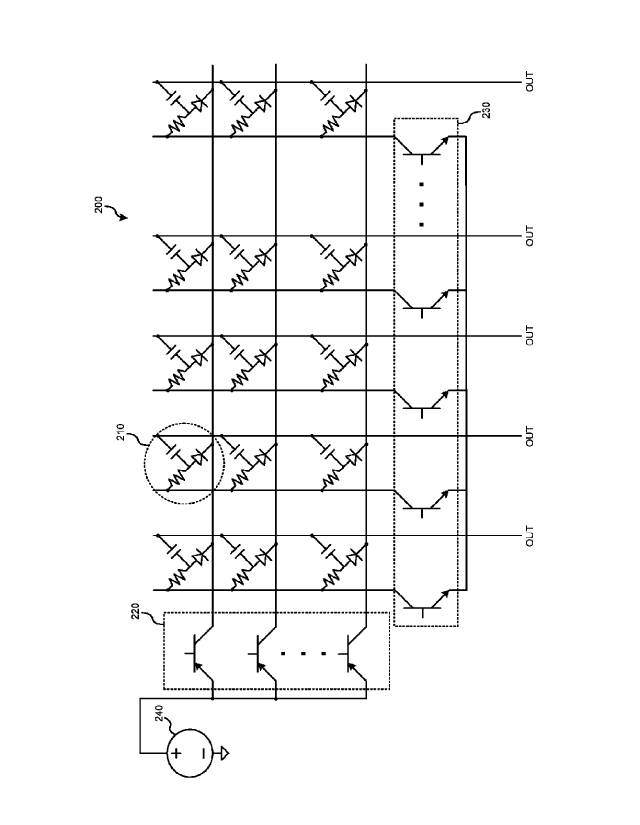
[0024] FIG. 2 is a simplified schematic diagram of a SiPM 200, according to
one
embodiment. As mentioned above, the SiPM 200 may be Incorporated into the
sensor
126 of FIG. 1. Here, the SiPM comprises an array of SPADs, wherein each SPAD
210
comprises resistive, capacitive, and photo sensitive elements, such as a
resistor, a
capacitor, and a photodiode, respectively. A person of ordinary skill in the
art will
appreciate typical values and/or other properties of these elements, which may
vary
depending on desired functionality. In some embodiments, for example, values
of
capacitance may be in the femtofarad range, and the resistance used in the
implementation could be over a wide range of values, depending on how the
array
design is optimized. For example, in some embodiments, the RC time constant of
the
capacitance acting against the quench resistor may be 10 nS or less. In these
embodiments, the resistor in series with each capacitor in FIG. 3 could be
anywhere
from zero (e.g., the resistor is omitted) to any value producing an RC time
constant
shorter than 10 nS. Other embodiments may have values above and/or below the
values
of this example.
6
CA 03017223 2018-09-07
WO 2017/180277 PCT/US2017/022199
[0025] It will be understood that the size of the array can vary, depending on
desired
functionality. That is, although the SiPM 200 illustrated in FIG. 2 has only
25 SPADs
illustrated, embodiments may have a larger or smaller number of SPADs,
depending on
desired functionality. Some embodiments may include, for example, hundreds,
thousands, or millions of SPADs, or more. In some embodiments, the entire SiPM
(and
optionally some of the additional circuitry shown in FIG. 2) may be
implemented on a
single semiconductor die. A person of ordinary skill in the art will
appreciate the fact
that various modifications can be made to the basic layout shown in FIG. 2. It
can be
further noted that, although the array is described as a SiPM 200, some
embodiments
may utilize photomultiplier arrays that utilize materials in addition or as an
alternative
to silicon.
[0026] In this embodiment, the SiPM 200 utilizes a plurality of row-select
transistors
220, as well as a plurality of column-select transistors 230, enabling
controlling
circuitry (such as a microprocessor or other processing circuit) to, by
activating these
transistors, select which SPADs in the array to use for sensing at a
particular moment.
In other words, these row-select transistors 220 and column-select transistors
230 can,
when activated, enable the controlling circuitry to "activate" a certain
subset of the
SiPM 200. Depending on desired functionality, manufacturing concerns, and/or
other
factors, these transistors could comprise NPN, PNP, N- or P-channel MOSFETs,
or
other types. Generally speaking, the size of the transistor may be big enough
to have a
on resistance between drain and source (RDS (on)) that is substantially
smaller than all
the quench resistors in parallel driven by that transistor, or small enough to
drive the
worst-case current needed by the row or column without more than a couple volt
drop.
In some embodiments, the voltage rating may be 30V or possibly more. However,
this
might vary depending on the photodetector used.
[0027] A SPAD and APD are both sensitive to the amount of bias voltage, which
is
set by bias voltage 240. Up to the breakdown voltage of the sensor, the gain
of the
SPAD and APD may be up to one electron per photon. Due to the efficiency of
the
sensor, the actual sensitivity may be substantially less than one electron per
photon. But
as the bias voltage increases to the breakdown voltage and beyond, the
sensitivity of the
APD and SPAD increases. For the arrangement of the SiPM SPAD microcells into a
matrix with the cathodes connected to rows and anodes connected to columns (as
shown
7
CA 03017223 2018-09-07
WO 2017/180277 PCT/US2017/022199
in FIG. 2), an area of high gain cells can be achieved by driving bias voltage
into rows
and columns to select an active area with high gain. The unselected cells
without the
high reverse bias have a very low gain while the active area (selected using
row- and
column-select transistors) has a gain of 201'5 or more. By selection of
multiple adjacent
rows and multiple adjacent columns, a desired square or rectangular area can
be
selected. Alternatively, some embodiments may be modified to allow a non-
rectangular
area may be selected.
[0028] The grouping of the SPAD cells can be column by column, row by row, or
an
arbitrary grouping of SPAD cells without regard to all the cells falling on
the same row
or column. It can be noted that the structure illustrated in FIG. 2 (as well
as the structure
of FIG. 3 below) will work if the anodes and cathodes are swapped, or rows and
columns are interchanged, as long as the polarity of drive at the SPAD cells
is reverse
biased.
[0029] The signal level from each SPAD may be quite high. This value depends
on
how many SPAD cells are connected together. For example, a single SPAD cell on
its
own may produce 5V, but if it is connected together in the same column with
1000
other SPAD cells, the loading of the other cells would drop that voltage to
5mV. other
embodiments may include higher or lower signal levels, depending on desired
functionality. In some embodiments, for smaller arrays of SPADs, all of the
capacitive
coupled cell outputs could be tied together to form a single output. Unbiased
SPAD
cells would create minimal response to being hit by a photon, while biased
cells will
have very high gain in terms of electrons per photon. As the array size gets
larger, the
capacitive coupled outputs may need to be broken into groups of microcells and
connected to a multiplexer or peak detector to prevent the signal level from
getting too
small due to voltage division amongst the connected cells. According to some
embodiments, if a set of switches or multiplexer is used, it may be at the
output of each
row in FIG. 3 (after the amplifier). Alternative embodiments may connect rows
before
each amplifier, but the signal from the active cells would be divided by the
total number
of cells. For extremely large arrays (e.g., arrays having several hundred
microcells or
more) the microcell groups could be amplified before being summed or
multiplexed.
This would further improve the signal to noise ratio by preventing the signal
from
becoming too weak before amplification.
8
CA 03017223 2018-09-07
WO 2017/180277 PCT/US2017/022199
[0030] It can be noted that, in FIG. 2, combining circuitry (such as
multiplexers
and/or amplifiers) is not shown, but may be used depending on desired
functionality.
The columns of the SiPM 200 each have an output (labeled "OUT" in FIG. 2) that
is
utilized to detect an output of the SiPM 200. If combining circuitry is
utilized, it could
combine one or more of these column outputs in a manner similar to the
embodiment
illustrated in FIG. 3.
[0031] FIG. 3 is a simplified schematic diagram of a SiPM 300, according to a
different embodiment. Here, the row-select transistors 320 and the column
select
transistors 330 are field-effect transistors (FETs). Other embodiments may
additionally
or alternatively include other types of transistors, depending on
manufacturing concerns,
desired functionality, and/or other factors. Each SPAD cell 310 differs
slightly from the
SPAD cells 210 of FIG. 2 in that the SPAD cells 310 of FIG. 3 include an
additional
output resistor element to reduce the effects of the capacitances of other
SPADs. The
lower-drive-strength signal is then amplified by a layer of trans impedance
amplifiers
(TIAs) 350 to increase drive strength before being passed on for detection. It
can be
noted that broadband amplifiers may be utilized in addition or as an
alternative to the
TIAs 350. It can be further noted that the SiPM 200 of FIG. 2 may utilize TIAs
350 in a
similar manner.
[0032] It should be noted, however, that such output resistive elements are
optional.
Embodiments utilizing bipolar junction transistors (BJTs) and/or FETs (such as
those
illustrated in FIGS. 2 and 3 respectively) may choose to include or omit such
additional
resistive elements, depending on desired functionality. The presence and/or
value of
such additional resistive elements can determine how an output pulse is
shaped. A
person having ordinary skill in the art will appreciate the factors that may
be utilized in
determining whether to include such additional resistive elements and what
values they
may be. In some embodiments, these resistive elements may simply be parasitic
resistive elements.
[0033] As with FIG. 2, embodiments may employ a larger or smaller number of
SPADs than is illustrated in the SiPM 300 illustrated in FIG. 3, depending on
desired
functionality. Again, embodiments may include, for example, hundreds,
thousands, or
millions of SPADs (or more).
9
CA 03017223 2018-09-07
WO 2017/180277 PCT/US2017/022199
[0034] As indicated previously, bias voltages 240 and 340 utilized in FIGS. 2
and 3,
respectively, can be chosen to determine the sensitivity of the SPADs, when
activated
(via row- and column-select transistors). In some embodiments, these bias
voltages may
be dynamic, enabling the SiPM to provide a variably-sensitive output depending
on, for
example, lighting conditions and/or other factors. Adjusting the bias voltage
of the
SPAD can change the sensitivity. The value of bias would likely be the same
for all of
the cells that are active (with the inactive cells unbiased). In other
embodiments, these
bias voltages may be static and/or factory set.
[0035] In a LIDAR application, the active rows and columns can be selected a
microsecond or more before the laser fires. As indicated previously, the row-
and/or
column-select signals used to activate the row-select transistors 220, 320 and
column-
select transistors 230, 330 can be generated by a processing unit or other
logic (e.g.,
processing unit 110 of FIG. 1) which may be in communication with and/or
control of
LIDAR transmission circuitry. As such, the processing unit or other logic may
know the
angle and/or spot size at which the LIDAR transmission circuitry will transmit
a laser
beam, and can select the rows and columns of the SPADs in the SiPM
corresponding to
the known angle and/or spot size. With the corresponding SPADs of the SiPM
activated when the LIDAR transmission circuitry fires the laser beam (and the
rest of
the SPADs remaining inactive), this will enable the SiPM to provide a higher
SNR,
resulting in more accurate LIDAR functionality.
[0036] FIG. 4 is a schematic diagram of a single SPAD, according to an
embodiment.
Here, the SPAD includes a current-limiting or bias/quench resistor 410, a high-
speed
capacitive structure 420, an optional output resistor 430, and a photodiode
440. As
indicated above, the input bias voltage can determine the sensitivity of the
photo
detection. A value for the current-limiting or bias/quench resistor 410 can be
determined
to limit the amount of current drawn when the photodiode 440 detects light.
Values for
the capacitive structure 420 and the optional output (decoupling) resistor 430
may be
determined by known techniques based on requirements for the circuitry
utilized to
combine and/or measure the output of the SPADs. According to some embodiments,
all
components of the SPAD (and indeed the entire SiPM and optionally supporting
circuitry, such as TIAs) may be implemented on a single semiconductor die.
Such a die
CA 03017223 2018-09-07
WO 2017/180277 PCT/US2017/022199
may be packaged in an integrated circuit (IC) package and utilized in larger
LIDAR or
other imaging devices.
[0037] FIG. 5 is a flow diagram of a method 500 of enabling the activation of
a
portion of a SiPM, according to some embodiments. It will be understood that
alternative embodiments may utilize additional or alternative functions from
those
illustrated in FIG. 5.
[0038] At block 510, in an array of SPADs having a plurality of rows and a
plurality
of columns, a portion of the array of SPADs is activated by providing a bias
voltage to
each SPAD in a subset of the rows and a subset of the columns. As illustrated
in the
embodiments shown in FIGS. 2-3, the bias voltage may be provided to the inputs
of
each SPAD by activating corresponding row-select and/or column-select
transistors. In
some embodiments, each SPAD comprises resistive, capacitive, and photo
detection
elements electrically connected with, a first input, a second input, and an
output, each
row of the plurality of rows has a corresponding row-select transistor that,
when
activated, causes the first inputs of each SPAD in the row to receive a bias
voltage, each
column of the plurality of rows has a corresponding column-select transistor
connected
with the second inputs of each SPAD in the column, and for each column, the
outputs of
each SPAD in the column are connected with a column output for that column. As
described previously, the activation of such transistors can be done with a
processing
unit (such as a microprocessor) and/or other logic configured to generate
signals to
activate the transistors. The rows and columns selected for activation may
correspond
with those SPADs that are expected to receive reflected laser light (this
determination
may also be made by the processing unit and/or other logic).
[0039] At block 520, and output of each of the columns of the array of SPADs
is read.
As indicated previously, this may be done by any of a variety of types of
circuitry. In
some embodiments, to ensure these outputs are read accurately, a multiplexor
may be
utilized to read only the outputs of the columns of SPADs selected at block
510.
Additionally or alternatively, these outputs may be amplified by TIAs and/or
other types
of amplifiers. In some embodiments, the outputs may be provided to a
processing unit
(such as the processing unit 110 of FIG. 1) and/or other processing circuitry.
[0040] As with other embodiments described herein, the method 500 illustrated
in
FIG. 5 may vary, depending on desired functionality. For example, transistors
utilized in
11
CA 03017223 2018-09-07
WO 2017/180277 PCT/US2017/022199
block 510 may comprise bipolar junction transistors (BJTs) and/or field-effect
transistors (FETs). Each SPAD may include an output resistor coupled with an
output
of the SPAD.
[0041] It will be apparent to those skilled in the art that substantial
variations may be
made in accordance with specific requirements. For example, customized
hardware
might also be used, and/or particular elements might be implemented in
hardware,
software (including portable software, such as applets, etc.), or both.
Further,
connection to other computing devices such as network input/output devices may
be
employed.
[0042] With reference to the appended figures, components that can include
memory
can include non-transitory machine-readable media. The term "machine-readable
medium" and "computer-readable medium" as used herein, refer to any storage
medium
that participates in providing data that causes a machine to operate in a
specific fashion.
In embodiments provided hereinabove, various machine-readable media might be
involved in providing instructions/code to processing units and/or other
device(s) for
execution. Additionally or alternatively, the machine-readable media might be
used to
store and/or carry such instructions/code. In many implementations, a computer-
readable medium is a physical and/or tangible storage medium. Such a medium
may
take many forms, including but not limited to, non-volatile media, volatile
media, and
transmission media. Common forms of computer-readable media include, for
example,
magnetic and/or optical media, punchcards, papertape, any other physical
medium with
patterns of holes, a RAM, a PROM, EPROM, a FLASH-EPROM, any other memory
chip or cartridge, a carrier wave as described hereinafter, or any other
medium from
which a computer can read instructions and/or code.
[0043] The methods, systems, and devices discussed herein are examples.
Various
embodiments may omit, substitute, or add various procedures or components as
appropriate. For instance, features described with respect to certain
embodiments may
be combined in various other embodiments. Different aspects and elements of
the
embodiments may be combined in a similar manner. The various components of the
figures provided herein can be embodied in hardware and/or software. Also,
technology
evolves and, thus, many of the elements are examples that do not limit the
scope of the
disclosure to those specific examples.
12
CA 03017223 2018-09-07
WO 2017/180277 PCT/US2017/022199
[0044] It has proven convenient at times, principally for reasons of common
usage, to
refer to such signals as bits, information, values, elements, symbols,
characters,
variables, terms, numbers, numerals, or the like. It should be understood,
however, that
all of these or similar terms are to be associated with appropriate physical
quantities and
are merely convenient labels. Unless specifically stated otherwise, as is
apparent from
the discussion above, it is appreciated that throughout this Specification
discussions
utilizing terms such as "processing," "computing," "calculating,"
"determining,"
"ascertaining," "identifying," "associating," "measuring," "performing," or
the like
refer to actions or processes of a specific apparatus, such as a special
purpose computer
or a similar special purpose electronic computing device. In the context of
this
Specification, therefore, a special purpose computer or a similar special
purpose
electronic computing device is capable of manipulating or transforming
signals,
typically represented as physical electronic, electrical, or magnetic
quantities within
memories, registers, or other information storage devices, transmission
devices, or
display devices of the special purpose computer or similar special purpose
electronic
computing device.
[0045] Terms, "and" and "or" as used herein, may include a variety of meanings
that
also is expected to depend at least in part upon the context in which such
terms are used.
Typically, "or" if used to associate a list, such as A, B, or C, is intended
to mean A, B,
and C, here used in the inclusive sense, as well as A, B, or C, here used in
the exclusive
sense. In addition, the term "one or more" as used herein may be used to
describe any
feature, structure, or characteristic in the singular or may be used to
describe some
combination of features, structures, or characteristics. However, it should be
noted that
this is merely an illustrative example and claimed subject matter is not
limited to this
example. Furthermore, the term "at least one of' if used to associate a list,
such as A,
B, or C, can be interpreted to mean any combination of A, B, and/or C, such as
A, AB,
AA, AAB, AABBCCC, etc.
[0046] Having described several embodiments, various modifications,
alternative
constructions, and equivalents may be used without departing from the spirit
of the
disclosure. For example, the above elements may merely be a component of a
larger
system, wherein other rules may take precedence over or otherwise modify the
application of the invention. Also, a number of steps may be undertaken
before, during,
13
CA 03017223 2018-09-07
WO 2017/180277 PCT/US2017/022199
or after the above elements are considered. Accordingly, the above description
does not
limit the scope of the disclosure.
14