Note: Descriptions are shown in the official language in which they were submitted.
CA 03018387 2018-09-19
WO 2017/173204 PCT/US2017/025249
MULTILEVEL BIPOLAR PULSER
RELATED APPLICATIONS
[0001] The present application is a continuation claiming the benefit under 35
U.S.C. 120 of
U.S. Patent Application Serial No. 15/087,914, filed March 31, 2016 under
Attorney Docket No.
B1348.70026US00 and entitled "MULTILEVEL BIPOLAR PULSER," which is hereby
incorporated herein by reference in its entirety.
BACKGROUND
[0002] Field
[0003] The present application relates to ultrasound devices for ultrasound
imaging and high
intensity focused ultrasound (HIFU).
[0004] Related Art
[0005] Some conventional ultrasound devices include pulsing circuits
configured to provide
pulses to an ultrasonic transducer. Often the ultrasonic transducer operates
in transmission and
reception.
BRIEF SUMMARY
[0006] Aspects of the present application provide an ultrasound-on-a-chip
device including
integrated circuitry having a pulser with feedback. Symmetric receive switches
are also
provided in the ultrasound-on-a-chip device and coupled to an output of the
ultrasonic
transducers to facilitate the use of multi-level pulsers to drive the
ultrasonic transducers.
[0007] Aspects of the present application relate to an ultrasound device
comprising a capacitive
ultrasonic transducer, a pulser having an input terminal and an output
terminal, the pulser
coupled, at the output terminal, to the capacitive ultrasonic transducer and
configured to provide
an input signal to the capacitive ultrasonic transducer, and a feedback
circuit coupled to the
output terminal and the input terminal of the pulser and configured to provide
a control signal to
the input terminal of the pulser based on a comparison of a detection signal,
representing or
derived from the input signal, to a threshold voltage.
[0008] Aspects of the present application relate to a method of operating an
ultrasound device
having a capacitive ultrasonic transducer, a pulser coupled to the capacitive
ultrasonic transducer
and a feedback circuit, the method comprising providing an input signal to the
capacitive
1
CA 03018387 2018-09-19
WO 2017/173204 PCT/US2017/025249
- 2 -
ultrasonic transducer with the pulser, deriving a detection signal from the
input signal, the
detection signal representing the input signal, providing a control signal,
with the feedback
circuit, to the pulser to control the providing of the input signal based on a
result obtained by
comparing the detection signal to a threshold voltage.
BRIEF DESCRIPTION OF DRAWINGS
[0009] Various aspects and embodiments of the application will be described
with reference to
the following figures. It should be appreciated that the figures are not
necessarily drawn to
scale. Items appearing in multiple figures are indicated by the same reference
number in all the
figures in which they appear.
[0010] FIG. 1 is a block diagram illustrating an ultrasound device including a
plurality of
pulsing circuits and a plurality of receiver switches, according to a non-
limiting embodiment of
the present application.
[0011] FIG. 2 is a block diagram illustrating a pulsing circuit coupled to a
capacitive ultrasonic
transducer, according to a non-limiting embodiment of the present application.
[0012] FIG. 3 is a block diagram illustrating a pulsing circuit comprising a
pulser and a
feedback circuit, according to a non-limiting embodiment of the present
application.
[0013] FIG. 4 is a block diagram illustrating the acts of a method to operate
a pulsing circuit
coupled to a capacitive ultrasonic transducer, according to a non-limiting
embodiment of the
present application.
[0014] FIG. 5A is a circuit diagram illustrating a resistive ladder configured
to generate a
plurality of threshold voltages, according to a non-limiting embodiment of the
present
application.
[0015] FIG. 5B is a circuit diagram illustrating a dividing circuit configured
to generate a
detection signal, according to a non-limiting embodiment of the present
application.
[0016] FIG. 6A illustrates a timing diagram showing an example signal provided
by the pulsing
circuit to the capacitive ultrasonic transducer, according to a non-limiting
embodiment of the
present application.
[0017] FIG. 6B illustrates a timing diagram showing an apodized signal
provided by the pulsing
circuit to the capacitive ultrasonic transducer, according to a non-limiting
embodiment of the
present application.
CA 03018387 2018-09-19
WO 2017/173204 PCT/US2017/025249
- 3 -
[0018] FIG. 7 is a block diagram illustrating a plurality of pulsing circuits
coupled to a plurality
of capacitive ultrasonic transducers, according to a non-limiting embodiment
of the present
application.
[0019] FIG. 8A is a block diagram illustrating an ultrasound device operating
in transmit mode,
according to a non-limiting embodiment of the present application.
[0020] FIG. 8B is a block diagram illustrating an ultrasound device operating
in receive mode,
according to a non-limiting embodiment of the present application.
[0021] FIG. 9 is a block diagram illustrating an ultrasound device comprising
a symmetric
switch, according to a non-limiting embodiment of the present application.
[0022] FIG. 10 illustrates a timing diagram showing control signals configured
to drive the
symmetric switch of FIG. 9, according to a non-limiting embodiment of the
present application.
[0023] FIG. 11 is a block diagram illustrating an alternative device
comprising a symmetric
switch, according to a non-limiting embodiment of the present application.
DETAILED DESCRIPTION
[0024] An ultrasound-on-a-chip device may include ultrasonic transducers
integrated with
circuitry on a semiconductor die, also referred to herein as a "chip." The
ultrasound-on-a-chip
device may be employed within an ultrasound probe to perform ultrasound
imaging, therapy
(e.g., high intensity focused ultrasound (HIFU)), or both. Thus, the circuitry
integrated with the
ultrasound transducers may support such functions and assume a form
appropriate for being
employed in a probe or other form factor, such as a stethoscope. The circuitry
may include
pulsing circuits which generate electrical pulses used to drive the ultrasonic
transducers of the
ultrasound-on-a-chip device to generate ultrasound signals appropriate for
imaging and/or HIFU.
The pulsing circuits may be digital, analog, or mixed analog-digital.
[0025] Aspects of the present application provide bipolar, multi-level pulsing
circuits with
feedback. Applicant has appreciated that ultrasound devices configured to
transmit unipolar
pulses exhibit limited dynamic range because the direct current (DC) component
associated with
the unipolar pulse may saturate the receiving circuit, thus deteriorating the
contrast of the image
produced. Unipolar pulses are those which only assume voltages greater than or
equal to zero
(0), or alternatively, voltages less than or equal to zero (0). Applicant has
appreciated that, by
contrast, the use of bipolar pulses limits the impact of the DC component and
thus provides
significantly increased dynamic range and image contrast compared to
ultrasound devices
CA 03018387 2018-09-19
WO 2017/173204 PCT/US2017/025249
- 4 -
utilizing unipolar pulses. Thus, aspects of the present application provide
ultrasound
complementary metal oxide semiconductor (CMOS) chips having circuitry
configured to
transmit bipolar pulses. Bipolar pulses can assume voltages that are greater
than, less than, or
equal to zero (0).
[0026] The use of multi-level pulsing circuits with feedback arises from
Applicant's
appreciation that the contrast of ultrasound images may be significantly
enhanced by performing
time-domain and space-domain apodization of the pulses transmitted to the
target being imaged.
Apodization may reduce the extent of the side-lobes associated with
transmitted pulses, thus
increasing the resolution of the image produced. The generation of temporally
and spatially
apodized pulses may be facilitated by the ability to control signals that can
assume multiple
values. Multi-level pulses of the type described herein can assume any value
selected from
among a set of selectable values, where the set may comprise at least three
values. The
generation of such multi-level pulses may require complicated pulser designs
where multiple
supply voltages are provided. Providing multiple supply voltages may be
impractical. This may
be especially true when the ultrasound device is to be disposed in a handheld
ultrasound probe
or other compact form, as additional off-chip supply circuits may be required.
Applicant has
appreciated that the use of feedback circuits may facilitate the generation of
multi-level pulses,
and the generation of apodized pulses, without resorting to multiple supply
voltages, thus
simplifying the design of the ultrasound device.
[0027] Aspects of the present application provide ultrasound devices including
a symmetric
switch coupling an ultrasonic transducer to receiving circuitry. While the use
of bipolar pulsing
circuits may be beneficial for at least the reasons described above, they can
also be detrimental
to the ultrasound device's receiving circuitry. The pulses generated by the
transmitting circuit
may inadvertently electrically couple directly to the receiving circuit, which
may not be
designed to withstand large positive and negative voltage spikes. As a
consequence, the
ultrasound device may be damaged if proper protection is not provided.
Applicant has
appreciated that a suitably positioned symmetric switch designed to block
positive and negative
voltage spikes associated with bipolar pulses may prevent damage to receiving
circuitry, thus
protecting the ultrasound device and facilitating use of bipolar pulsing
circuits.
[0028] The CMOS circuitry features described above may facilitate creation of
an ultrasound-
on-a-chip device suitable for performing ultrasound imaging and/or HIFU in a
commercially
valuable form factor.
CA 03018387 2018-09-19
WO 2017/173204 PCT/US2017/025249
- 5 -
[0029] The aspects and embodiments described above, as well as additional
aspects and
embodiments, are described further below. These aspects and/or embodiments may
be used
individually, all together, or in any combination of two or more, as the
application is not limited
in this respect.
[0030] As described above, aspects of the present application provide an
ultrasound device
having a bipolar, multi-level pulsing circuit and a symmetric switch coupling
the bi-polar, multi-
level pulsing circuit to receive circuitry. FIG. 1 illustrates the general
architecture of an
ultrasound device which may include such features in accordance with aspects
of the present
application. The ultrasound device 100 has a plurality of capacitive
ultrasonic transducers
1011...101N, where N is an integer. Ultrasound device 100 may comprise a
plurality of circuitry
channels 1021...102N. Circuitry channels 1021 ...102N may be electrically
connected to a
respective capacitive ultrasonic transducer 1011 ...101N. Ultrasound device
100 may further
comprise analog-to-digital converter (ADC) 111.
[0031] The capacitive ultrasonic transducers are sensors in some embodiments,
producing
electrical signals representing received ultrasound signals. The capacitive
ultrasonic transducers
may also transmit ultrasound signals in some embodiments. The capacitive
ultrasonic
transducers may be capacitive micromachined ultrasonic transducers (CMUTs) in
some
embodiments. However, other types of capacitive ultrasonic transducers may be
used in other
embodiments.
[0032] The circuitry channels 1021 ...102N may include transmit circuitry,
receive circuitry, or
both. The transmit circuitry may include transmit decoders 105i...105N coupled
to respective
pulsing circuits 103i...103N. The pulsing circuits 103i...103N may control the
respective
ultrasonic transducers 101i...101N to emit ultrasound signals.
[0033] Aspects of the present application relate to pulsing circuits 1031
...103N. In some
embodiments, pulsing circuits 1031 ...103N may be configured to generate
bipolar pulses. In
some embodiments, pulsing circuits 103i...103N may be configured to generate
multi-level
pulses. As will be described further below, pulsing circuits 103i... 103N may
include pulsers
plus additional circuitry in some embodiments. In some embodiments, the
pulsing circuits
1031 ...103N may include pulsers and feedback circuitry.
[0034] The receive circuitry of the circuitry channels 102i... 102N may
receive the electrical
signals output from respective capacitive ultrasonic transducers 1011...101N.
In the illustrated
example, each circuitry channel 1021...102N includes a respective receive
switch 1071 ...107N
CA 03018387 2018-09-19
WO 2017/173204 PCT/US2017/025249
- 6 -
and a receiving circuit 109i...109N. The receive switches 107i...107N may be
controlled to
activate/deactivate readout of an electrical signal from a given ultrasonic
transducer 1011...101N.
The receiving circuits 1091 ...109N may comprise current-to-voltage
converters. The current-to-
voltage converters may comprise trans-impedance amplifiers (TIAs), and for
that reason the
receiving circuits 109i...109N are illustrated as TIAs, although additional
and/or alternative
circuitry may constitute the receiving circuits..
[0035] Aspects of the present application relate to receive switches 1071
...107N. In some
embodiments, receive switches 1071 ...107N may comprise symmetric switches
configured to
block voltage spikes exhibiting positive and/or negative voltages. Receive
switches 1071...107N
may be configured to form an open circuit to electrically decouple the
receiving circuitry from
the transmitting circuitry and from the capacitive ultrasonic transducer
during a transmit mode.
Receive switches 1071 ...107N may be further configured to form a short
circuit to electrically
couple the receive circuitry to the capacitive ultrasonic transducer during a
receive mode.
[0036] Ultrasound device 100 may further comprise ADC 111. ADC 111 may be
configured to
digitize the signals received by capacitive ultrasonic transducers 1011
...101N. The digitization of
the various received signals may be performed in series or in parallel. While
a single ADC is
illustrated, and thus is shown as being shared by multiple circuitry channels,
alternative
embodiments provide for one ADC per circuitry channel.
[0037] While FIG. 1 illustrates a number of components as part of a circuit of
an ultrasound
device, it should be appreciated that the various aspects described herein are
not limited to the
exact components or configuration of components illustrated.
[0038] The components of FIG. 1 may be located on a single substrate or on
different substrates.
When located on a single substrate, the substrate may be a semiconductor
substrate as an
example, such as a silicon substrate, and components may be monolithically
integrated thereon.
When the illustrated components are not on the same substrate, the capacitive
ultrasonic
transducers 1011...101N may be on a first substrate and the remaining
illustrated components
may be on a second substrate, as an example. As a further alternative, the
ultrasonic transducers
and some of the illustrated circuitry may be on the same substrate, while
other circuitry
components may be on a different substrate. When multiple substrates are used,
they may be
semiconductor substrates, such as silicon substrates.
CA 03018387 2018-09-19
WO 2017/173204 PCT/US2017/025249
-7 -
[0039] According to an embodiment, the components of FIG. 1 form part of an
ultrasound
probe. The ultrasound probe may be handheld. In some embodiments, the
components of FIG.
1 form part of an ultrasound patch configured to be worn by a patient.
[0040] FIG. 2 illustrates an example of a pulsing circuit 103 which may serve
as any of the
pulsing circuits 103i...103N of FIG. 1, according to some non-limiting
embodiments. In some
embodiments, pulsing circuit 103 may comprise pulser 220 and feedback circuit
230. Pulsing
circuit 103 may have an output terminal electrically connected to capacitive
ultrasonic
transducer 101, and may be configured to provide an input signal 240 to
capacitive ultrasonic
transducer 101. In some embodiments, pulser 220 may be configured to generate
bipolar pulses,
that may assume positive and/or negative values in addition to zero. By
generating bipolar
pulses, pulser 220 can diminish, or suppress, any DC component associated with
the pulses. As
noted previously, transmitting pulses having DC components may degrade the
quality of the
image produced by ultrasound device 100. Accordingly, compared to the passband
component,
DC components may attenuate significantly less while propagating through the
medium being
imaged. Consequently, the receiving circuit may receive a signal having a DC
component that is
significantly greater than the passband component. As a result, the receiving
circuit may saturate
thus limiting the dynamic range of the image.
[0041] In some embodiments, the feedback circuit may be configured to control
the pulser to
generate multi-level pulses. Multi-level pulses of the type described herein
can assume any value
selected from among a set of selectable values, where the set may comprise at
least three values
and in at least some embodiments may include four or more values (e.g.,
between 3 and 30
values, between 4 and 20 values, between 4 and 10 values, or any number within
those ranges).
The use of multi-level pulses may enable the optimization of the pulse's
envelope to maximize a
parameter of the ultrasound image being formed. For example, the envelope of
the pulses may
be engineered to maximize image contrast. In particular, by using time-domain
apodization, the
resulting frequency content of the pulses may exhibit a large main-lobe and
suppressed side-
lobes, thus increasing imaging resolution. Time-domain apodization requires
pulses exhibiting
as many voltage levels as possible to produce nearly-continuous window
functions. However,
the generation of pulses having a large number of levels can require complex
pulsing circuits.
Therefore the number of levels should be chosen to maximize the ability to
perform time-
domain apodization while keeping the pulsing circuits relatively simple and
compact. In some
CA 03018387 2018-09-19
WO 2017/173204 PCT/US2017/025249
- 8 -
embodiments, pulser 220 may be configured to generate multi-level pulses
having between 3
and 30 levels, between 5 and 10 levels, or between any suitable value or range
of values.
[0042] The use of multi-level pulses may also enable space-domain apodization.
To perform
space-domain apodization the various capacitive ultrasonic transducers would
have to be driven
with input signals having space-dependent amplitudes. Provision of input
signals having space-
dependent amplitudes may be facilitated by having access to a plurality of
reference voltages.
[0043] In some embodiments, feedback circuit 230 may be configured to
facilitate multi-level
pulse generation. In particular, feedback circuit 230 may be configured to
provide a plurality of
reference voltages. As noted previously, the use of feedback circuits of the
type described herein
may facilitate the design of multi-level pulsers without resorting to multiple
supply voltages. In
some embodiments it may be undesirable to include multiple supply voltages,
which may lead to
sizeable ultrasound probes that may be difficult to fit in a handheld form
factor. Contrarily,
feedback circuits of the type described herein may provide compact circuitry
to generate
reference voltages and may be easily included in handheld ultrasound probes.
[0044] The output terminal of feedback circuit 230 may be electrically coupled
to the input
terminal of pulser 220. The input terminal of feedback circuit 230 may be
electrically coupled to
the output terminal of pulser 220. The input terminal of feedback circuit 230
may be configured
to receive a detection signal 241 representing input signal 240. In some
embodiments, input
signal 240 and detection signal 241 are voltages. In some embodiments,
detection signal 241
may be derived from input signal 240. In some embodiments, detection signal
241 may be
proportional to input signal 240. Feedback circuit 230 may compare detection
signal 241 to a
threshold voltage. In some embodiments, said threshold voltage may be selected
from among a
set of selectable threshold voltages.
[0045] Based on the outcome of the comparison, feedback circuit 230 may
provide a control
signal 242 to the input terminal of pulser 220. In some embodiments, feedback
circuit 230 may
be configured to determine whether detection signal 241 is greater than, less
than or equal to a
threshold voltage. In some embodiments, feedback circuit 230 may be configured
to determine
whether detection signal 241 is within a range of the threshold voltage, such
as within 10% of
the threshold voltage, within 5% of the threshold voltage, or within any
suitable range. Based on
the value of detection signal 241 relative to the threshold voltage, feedback
circuit 230 may
control pulser 220 to hold the present value of input signal 240 or to vary
input signal 240. By
way of example and not limitation, if the value of detection signal 241 is
less than the threshold
CA 03018387 2018-09-19
WO 2017/173204 PCT/US2017/025249
- 9 -
voltage, feedback circuit 230 may control pulser 220 to increase the value of
input signal 240
until detection signal 241 is equal to, or within a range of, the threshold
voltage. If the value of
detection signal 241 is greater than the threshold voltage, feedback circuit
230 may control
pulser 220 to decrease the value of input signal 240 until detection signal
241 is equal to, or
within a range of, the threshold voltage.
[0046] In some embodiments, the capacitance associated with capacitive
ultrasonic transducer
101 may retain an electric charge to maintain a constant voltage across its
terminals when
detection signal 241 has reached the selected threshold voltage. When
detection signal 241 is
less than the threshold voltage, pulser 220 may be controlled to charge the
capacitance
associated with capacitive ultrasonic transducer 101, thus increasing input
signal 240. When
detection signal 241 is greater than the threshold voltage, pulser 220 may be
controlled to
discharge, or negatively charge, the capacitance associated with capacitive
ultrasonic transducer
101, thus decreasing input signal 240.
[0047] In some embodiments, feedback circuit 230 may control pulser 220
asynchronously.
Accordingly, control signal 242, input signal 240 and detection signal 241 may
be allowed to
vary at any moment in time. In some embodiments, pulsing circuit 100 may be
timed by a clock
signal. However, control signal 242 may still be allowed to vary during
periods of time that are
not defined by the clock signal.
[0048] In some embodiments, capacitive ultrasonic transducer 101 may be
coupled to bias
circuitry (not shown) and may be configured to receive a bias voltage having
an absolute value
that is greater than zero. The bias voltage may have an absolute value that is
between 10V and
100V, between 30V and 80V, or between any suitable values or range of values.
In some
embodiments, biasing capacitive ultrasonic transducers may lead to responses
exhibiting
increased degrees of linearity.
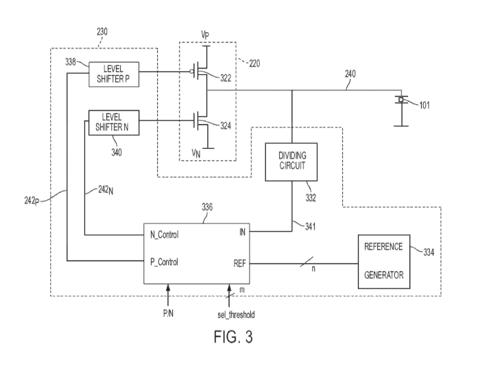
[0049] FIG. 3 is a non-limiting detailed implementation of the pulsing circuit
of FIG. 2. In some
embodiments, pulser 220 may comprise two transistors, such as 322 and 324.
However pulser
220 is not limited in this respect, and any suitable number of transistors may
be used. The
transistors may comprise metal-oxide-semiconductor field effect transistors
(MOSFETs),
junction field effect transistors (JFETs), bipolar junction transistors
(BJTs), metal-
semiconductor field effect transistors (MESFETs), insulated gate field effect
transistors
(IGFETs), laterally diffused metal-oxide-semiconductor transistors (LDMOS), or
any suitable
combination thereof. Pulser 220 may comprise transistor 322 and transistor
324. Transistor 322
CA 03018387 2018-09-19
WO 2017/173204 PCT/US2017/025249
- 10 -
may have one type of conductivity that is different from the type of
conductivity of transistor
324. For example, transistor 322 may have a conductivity that is based on
drift currents
sustained by holes moving under the effect of an electric field. Transistor
324 may have a
conductivity that is based on drift currents sustained by electrons moving
under the effect of an
electric field. In some embodiments, transistor 324 may be an nMOSFET and
transistor 322 may
be a pMOSFET. The transistors may be configured such that the drain of nMOS
transistor 324 is
connected to the drain of pMOS transistor 324. The drains may be further
connected to a
terminal of capacitive ultrasonic transducer 101. The source of nMOS
transistor 324 may be
connected to a supply voltage VN. In some embodiments, VN may be less than
zero. VN may be
between -100V and -1V, between -50V and -20V, or between any suitable values
or range of
values. The source of pMOS transistor 322 may be connected to a supply voltage
Vp. In some
embodiments, Vp may be greater than zero. Vp may be between 1V and 100V,
between 20V and
50V, or between any suitable values or range of values. The voltages provided
to the gates of
transistors 322 and 324 may be generated by feedback circuit 230 of FIG. 2.
[0050] In some embodiments, feedback circuit 230 may comprise controller 336,
dividing
circuit 332 and reference generator 334. In some embodiments, feedback circuit
230 may further
comprise level shifter 338 and level shifter 340. Dividing circuit 332 may be
configured to
receive the voltage corresponding to input signal 240 and to output detection
signal 341.
Dividing circuit 332 may be configured to provide a detection signal 341 that
is proportional to
input signal 240. Detection signal 341 may be provided to controller 336
through the input
terminal labelled "In".
[0051] Reference generator 334 may be configured to provide a set of
selectable threshold
voltages to the terminal labelled "Ref" of controller 336. In some
embodiments, reference
generator 334 is connected to controller 336 through n connectors, and is
configured to provide
n threshold voltages through corresponding connectors, where n may assume any
suitable value
greater than two. The threshold voltages may be equal to, greater, or less
than zero.
[0052] In some embodiments, feedback circuit 230 may be digitally controlled,
and controller
336 may comprise a digital controller. Controller 336 may be configured to
control pulser 220 to
hold, increase or decrease the voltage corresponding to input signal 240 based
on a comparison
of detection signal 341 with a threshold voltage, selected from among the n
threshold voltages.
Controller 336 may select a threshold voltage from the n threshold voltages
provided by
reference generator 334. The threshold voltage may be digitally selected
through signal
CA 03018387 2018-09-19
WO 2017/173204 PCT/US2017/025249
- 11 -
sel threshold. Signal sel threshold may comprise m bits, where m is such that
n is equal to, or
less than, 2'. Each bit combination may select one threshold voltage from the
n threshold
voltages. By way of example and not limitation, a sel threshold sequence equal
to 000 may
select the least of 8 threshold voltages, and a sel threshold sequence equal
to 111 may select the
largest of 8 threshold voltages. Furthermore, signal sel threshold may be
varied asynchronously.
[0053] In some embodiments, dividing circuit 332 may provide a detection
signal 341 that is
proportional to input signal 240 by a scaling factor. In such embodiments,
reference generator
334 may be configured to provide a set of threshold voltages that are scaled
to input signal 240
by the same scaling factor. Consequently, detection signal 341 may be directly
compared to the
selected threshold voltage without having to further scale one of the two
signals.
[0054] In some embodiments, signal p/n may be used to control the status of
transistors 322 and
324. In some embodiments, p/n may be a single bit signal. Signal p/n may be
set to "p" to
activate transistor 322, or to "n" to activate transistor 324. However any
suitable number of bits
configured to control the status of transistors 322 and 324 may also be used.
The value of the
single bit may cause either transistor 322 or transistor 324 to turn into a
conductive state,
whether in linear or saturation mode. In such embodiment, only one transistor
at a time may be
set to a conductive state.
[0055] Based on the value of sel threshold and p/n, controller 336 may output
control signals
242p and 242N, through the output terminals labelled "N control" and "P
control". Together,
control signals 242p and 242N, may represent control signal 242 illustrated in
FIG. 2. Signal
242p may comprise a single bit, in some embodiments, configured to control the
state of pMOS
transistor 322. Signal 242N may comprise a single bit, in some embodiments,
configured to
control the state of nMOS transistor 324. The two transistors may be allowed
to be in a cutoff
state at the same time.
[0056] In some embodiments, control signals 242p and 242N may directly drive
the gates of
transistors 322 and 324 respectively. In other embodiments, as shown in FIG.
3, control signals
242p and 242N may be coupled to the input terminals of level shifter 338 and
level shifter 340,
respectively. The output terminals of level shifter 338 and level shifter 340
may be coupled to
the gates of transistors 322 and 324 respectively. Level shifters 338 and
level shifter 340 may be
configured to adapt the voltages generated by controller 336 to voltages
compatible to transistors
322 and 324 to drive the transistors into their cutoff or conductive state,
based on signals 242p
and 242N.
CA 03018387 2018-09-19
WO 2017/173204 PCT/US2017/025249
- 12 -
[0057] When detection signal 341 is less than the selected threshold voltage,
controller 336 may
be configured to output control signals 242p and 242N with values suitable to
turn pMOS
transistor 322 into a conductive state and nMOS 324 transistor into a cutoff
state. In this case, an
electric current flowing from voltage supply Vp to capacitive ultrasonic
transducer 101 may
charge capacitive ultrasonic transducer 101 until detection signal 341 reaches
the selected
threshold voltage, or a predetermined range of the selected threshold voltage.
[0058] When detection signal 341 is greater than the selected threshold
voltage, controller 336
may be configured to output control signals 242p and 242N with values suitable
to turn nMOS
transistor 324 into a conductive state and pMOS transistor 322 into a cutoff
state. In this case, an
electric current flowing from capacitive ultrasonic transducer 101 to voltage
supply VN may
discharge, or negatively charge, capacitive ultrasonic transducer 101 until
detection signal 341
reaches the selected threshold voltage, or a predetermined range of the
selected threshold
voltage.
[0059] When detection signal 241 is equal or within a predetermined range of
the selected
threshold voltage, pMOS transistor 322 and nMOS transistor 324 may be
controlled through
signals 242p and 242N to both turn into a cutoff state. In this case, no
electric current would flow
to or from capacitive ultrasonic transducer 101. Consequently, capacitive
ultrasonic transducer
101 may retain an electric charge, thus holding the target voltage
corresponding to the selected
threshold voltage across its terminals.
[0060] Because, as described above, in at least some embodiments it may be
desirable for the
ultrasound transducers 101 to hold their charge, in such embodiments the
ultrasound transducers
may be capacitive. By contrast, the use of resistive ultrasound transducers
may not operate
properly in such situations.
[0061] While controller 336 may be configured to control pulser 220 based on
the signals p/n
and sel threshold in the non-limiting embodiment described in connection with
FIG. 3, pulsing
circuit 103 is not limited in this respect. Accordingly, any signal, or
combination of signals,
configured to control pulser 220 to hold, increase or decrease input signal
240 until a threshold
voltage, or a range of the threshold voltage, is reached, may also be
employed.
[0062] FIG. 4 illustrates a method to operate a pulsing circuit to drive a
capacitive ultrasonic
device, according to some non-limiting embodiments. The method of FIG. 4 may
be performed
in connection with the pulsing circuit of FIG.2 or the pulsing circuit of FIG.
3. Method 400
starts at act 402, where a threshold voltage may be selected from among a set
of n selectable
CA 03018387 2018-09-19
WO 2017/173204 PCT/US2017/025249
- 13 -
threshold voltages, where n may assume any suitable value greater than two. In
some
embodiments the threshold voltage may be selected through a digital signal
having m bits,
where n is equal to, or less than, 2m
[0063] Method 400 continues to act 404, where an input signal, such as input
signal 240, may be
provided by pulser 220 to capacitive ultrasonic transducer 101. According to
one aspect of the
present application, pulser 220 may be configured to provide a bipolar input
signal, which may
exhibit positive and/or negative voltages. Bipolar input signals of the type
described herein may
lead to echo signals that do not saturate the receiving circuit of the
ultrasound device.
[0064] According to another aspect of the present application, pulser 220 may
be configured to
provide a multi-level pulse, which may exhibit values selected from among
multiple selectable
values. Pulsing circuits capable of generating multi-level pulses may
facilitate time-domain and
space-domain apodization, which may lead to enhanced image contrast. The
generation of multi-
level pulses of the type described herein may be facilitated by feedback
circuits designed to
provide a threshold voltage selected from a set of threshold voltages, without
resorting to
additional voltage supply circuits that may render handheld ultrasound probes
more sizeable.
[0065] At act 406, a detection signal, such as detection signal 341, may be
derived from input
signal 240. Detection signal 341 may represent input signal 240. Accordingly,
detection signal
341 may be equal, or proportional, to input signal 240.
[0066] At act 408, detection signal 341 may be compared to the threshold
voltage selected at act
402. In some embodiments detection signal 341 is proportional to input signal
240 by a scaling
factor. In such embodiments, the threshold voltage may be scaled to input
signal 240 by the
same scaling factor. As a result of the comparison, detection signal 341 may
be equal to, greater
than, or less than the threshold voltage.
[0067] At act 410, based on the result of the comparison performed at act 408,
a control signal
242 may be provided to pulser 220 to control input signal 240. The control
signal may be
provided by feedback circuit 230. Feedback circuit 230 may be controlled
digitally. At act 412,
if detection signal 341 is less than the selected threshold voltage, control
signal 242 may control
pulser 220 to increase the voltage corresponding to input signal 240. In some
embodiments,
control signal 242 may turn pMOS transistor 322 into a conductive state to
charge the
capacitance associated to capacitive ultrasonic transducer 101.
[0068] At act 412, if detection signal 341 is greater than the selected
threshold voltage, control
signal 242 may control pulser 220 to decrease the voltage corresponding to
input signal 240. In
CA 03018387 2018-09-19
WO 2017/173204 PCT/US2017/025249
- 14 -
some embodiments, control signal 242 may turn nMOS transistor 324 into a
conductive state to
discharge, or negatively charge, the capacitance associated to capacitive
ultrasonic transducer
101.
[0069] In either case, method 400 may return back to act 406 and method 400
may repeat until
detection signal 341 is equal or within a predefined range of the selected
threshold voltage.
[0070] At act 412, if detection signal 341 is found to be equal or within a
predefined range of
the selected threshold voltage, control signal 242 may control pulser 220 to
hold the current
value of input signal 240. In some embodiments, control signal 242 may turn
nMOS transistor
324 and pMOS transistor 322 into a cutoff state to allow the capacitance
associated with
capacitive ultrasonic transducer 101 to retain the current electric charge.
The predefined range
may be defined as 10% within the selected threshold voltage, 5% within the
selected threshold
voltage, or within any suitable range.
[0071] Once input signal 240 has reached the voltage corresponding to the
threshold voltage,
another threshold voltage may be selected from among the n selectable
threshold voltages at act
414. If another threshold voltage is selected at act 414, method 400 may
repeat from act 404 for
the newly selected threshold voltage. The selection of the new threshold
voltage may be
performed asynchronously. Otherwise, if no new threshold voltage is selected,
method 400 may
end at act 416.
[0072] FIG. 5A illustrates the circuit diagram of the reference generator of
FIG. 3, according to
some non-limiting embodiments. Reference generator 334 may comprise a
resistive ladder,
configured to generate n threshold voltages reb...refn, where n may assume any
value greater
than two. The resistive ladder may comprise n+1 resistors 5341...534õ i
connected in series, in
some embodiments. Resistor 534i may be coupled to supply voltage VH. Supply
voltage VH may
be equal to supply voltage Vp, shown in FIG. 3. Resistor 534õ i may be coupled
to supply
voltage VL. Supply voltage VL may equal supply voltage VN, shown in FIG. 3. In
some
embodiments, the n+1 resistors may all have equal resistances to divide the
voltage range
corresponding to VH-VL into n equal segments. In other embodiments, resistors
5342...534n+1
may have resistances equal to R, while resistor 5341 may have a resistance
equal to xR, where x
may assume any value between 0.01 and 100. However, other values are also
possible. In such
embodiments, a scaled voltage range proportional to VH-VL may be divided into
n equal
segments.
CA 03018387 2018-09-19
WO 2017/173204 PCT/US2017/025249
- 15 -
[0073] FIG. 5B illustrates the circuit diagram of the dividing circuit of FIG.
3, according to
some non-limiting embodiments. The dividing circuit may comprise a capacitive
divider,
configured to generate a detection signal 341 that is proportional to input
signal 240. The
capacitive divider may comprise capacitor 532 and capacitor 533. Capacitor 532
may have one
terminal coupled to the output of pulser 220 and one terminal coupled to an
input of controller
336. In some embodiments, capacitor 532 may be configured to receive input
signal 240
generated from by pulser 220. Capacitor 533 may have one terminal coupled to
the same input
of controller 336 and one terminal coupled to supply voltage Vc. In some
embodiments,
capacitor 336 may be configured to receive a scaled version of input signal
240 In some
embodiments, supply voltage Vc may be equal to supply voltage VN shown in FIG.
3. The
capacitance of capacitors 532 and 533 may be configured to scale detection
signal 341 by the
same scaling factor by which the threshold voltages of FIG. 5A are scaled. In
such
embodiments, detection signal 341 may be directly compared to a threshold
voltage selected
from among the n threshold voltage without having to scale any of the two
signals first.
[0074] FIG. 6A illustrates a timing diagram showing an example signal provided
by the pulsing
circuit to the capacitive ultrasonic transducer, according to a non-limiting
embodiment of the
present application. In particular, timing diagram 600 illustrates an
exemplary target signal 602
and an exemplary input signal 240. In the non-limiting embodiment presented in
connection
with FIG. 6A, a threshold voltage may be selected from among seven threshold
voltages. Target
signal 602 represents the signal to be followed by input signal 240. When
input signal 240 is
equal to target signal 602, for example at ti, then detection signal 341 is
equal to the current
threshold voltage. In this case, feedback circuit 230 may control pulser 220
to keep input voltage
240 constant at the current value. When input voltage 240 is less than target
voltage 602, for
example at t2, feedback circuit 230 may control pulser 220 to increase input
voltage 240 until the
current target voltage is reached. When input voltage 240 is greater than
target voltage 602, for
example at t3, feedback circuit 230 may control pulser 220 to decrease input
voltage 240 until
the current target voltage is reached. In some embodiments, target signal 602
may be varied
asynchronously. Consequently the duration of each segment of target voltage
602 may be set
independently from the duration of the other segments.
[0075] In some embodiments, pulsing circuit 103 may be configured to generate
an input signal
240 having a DC component that is greater than zero. The extent of the DC
component may be
chosen to bias the receiving circuit without letting it reach saturation.
CA 03018387 2018-09-19
WO 2017/173204 PCT/US2017/025249
- 16 -
[0076] In some embodiments, input signal 240 may overshoot target signal 602
(not shown). To
mitigate the occurrence of such an overshoot, feedback circuit 230 may be
configured to skew
the threshold voltage. In some embodiments, the threshold voltage may be
skewed by adding (or
subtracting) a voltage offset to the threshold voltage. For example, if the
desired output voltage
is x volts, the threshold voltage may be set to y volts, such that the
difference between x and y is
equal to the overshooting voltage. In some embodiments, the threshold voltage
may be skewed
through a non-uniform resistive ladder.
[0077] FIG. 6B illustrates a timing diagram showing an apodized signal
provided by the pulsing
circuit to the capacitive ultrasonic transducer, according to a non-limiting
embodiment of the
present application. In particular, timing diagram 620 illustrates an apodized
target signal 604
and an apodized input signal 240. Feedback circuit 230 may be configured to
perform time-
domain apodization of input signal 240 based on a Gaussian window, a Hamming
window, a flat
top window, a cosine window, or any suitable window function. Multi-level
pulses of the type
described herein provide a sufficient degree of granularity to faithfully
generate continuous
window functions.
[0078] FIG. 7 is a block diagram illustrating a plurality of pulsing circuits
coupled to a plurality
of capacitive ultrasonic transducers, according to a non-limiting embodiment
of the present
application. In some embodiments, capacitive ultrasonic transducers 1011,
1012, 1013...101N
may be disposed to form a 1D array. In other embodiments, capacitive
ultrasonic transducers
1011...101N may be disposed to form a 2D array. Capacitive ultrasonic
transducers 1011...101N
may be coupled to the output terminal of a respective pulser among pulsers
220i, 2202,
2203...220N. Feedback circuits 230i, 2302, 2303,...230N may be coupled to the
input terminal
and to the output terminal of a respective pulser among pulsers 2201...220N.
In some
embodiments, feedback circuits 2301...230N may be separate circuits. In other
embodiments,
feedback circuits 2301...230N may be part of a single circuit, configured to
control pulsers
2201...220N. As illustrated in FIG. 7, feedback circuits 2301...230N may
control pulsers
2201...220N to generate input signal 7401, 7402, 7403,...740N that exhibit
amplitudes that are
space-dependent. In some embodiments the feedback circuits may control the
pulsers to perform
space-domain apodization of the input signals. By way of example and not
limitation, input
signals 7401...740N may exhibit amplitudes that are larger at the center of
the array and decay,
following a predefined profile, towards the edge of the array. The space-
domain apodization
function may be a Gaussian window, a Hamming window, a flat top window, a
cosine window,
CA 03018387 2018-09-19
WO 2017/173204 PCT/US2017/025249
- 17 -
or any suitable window function. Space-domain apodization may be performed
over one spatial
dimension or two spatial dimensions. By performing space-domain apodization,
the aperture of
the array may be effectively varied, thus providing means to optimize the
spatial profile of the
emitted ultrasound wave. In some embodiments, the spatial profile may be
optimized to
minimize spatial side-lobes. Ultrasound devices capable of emitting spatial
profiles that have
minimal, or suppressed, side-lobes exhibit enhanced spatial resolution and
hence increased
image contrast.
[0079] In some embodiments, capacitive ultrasonic transducer 101 may be
connected to transmit
and receive circuitry. During transmission, the bipolar input signal generated
by the pulsing
circuit may inadvertently couple to the receiving circuit. The receiving
circuit may comprise, in
some embodiments, components that are not designed to withstand large positive
and negative
voltage spikes of the type generated with pulser 220. Accordingly, coupling
bipolar pulses
directly into the receiving circuit may have the effect of damaging one or
more components.
[0080] According to aspects of the present application, a symmetric switch
configured to
decouple the receiving circuit from the transmitting circuit while the bipolar
pulses are being
generated is provided. As used herein, a symmetric switch is a transistor-
based switch which has
input and output terminals of the same type. For example, the input and output
terminals of the
switch may both be sources, both drains, both emitters, both collectors, or
other terminal types.
FIG. 8A and FIG. 8B are block diagrams illustrating an ultrasound device
operating in transmit
mode and receive mode respectively, according to a non-limiting embodiment of
the present
application. Symmetric switch 107 may have an input terminal connected to the
output terminal
of pulsing circuits 103. In some embodiments, the input terminal of symmetric
switch 107 may
be connected to the output terminal of pulser 220 of pulsing circuit 103. The
input terminal of
symmetric switch 107 may be further connected to a terminal of capacitive
ultrasonic transducer
101. In some embodiments, the input terminal of symmetric switch 107 may be
coupled between
the output terminal of pulser 220 and a terminal of capacitive ultrasonic
transducer 101.
Symmetric switch may also have an output terminal coupled to the input
terminal of receiving
circuit 109. In some embodiments, receiving circuit 109 comprises a current-to-
voltage
converter configured to convert the current generated by capacitive ultrasonic
transducer 101 in
response to receiving an echo signal. In some embodiments, the current-to-
voltage converter
may comprise a trans-impedance amplifier (TIA).
CA 03018387 2018-09-19
WO 2017/173204 PCT/US2017/025249
- 18 -
[0081] As illustrated in FIG. 8A, in transmit mode (TX mode), symmetric switch
107 may be
configured to provide high impedance to decouple the pulse generated by
pulsing circuit 103
from receiving circuit 109. In some embodiments, symmetric switch 107 may be
configured to
operate as an open circuit during transmit mode. Arrow 801 may represent the
signal path
corresponding to input signal 240 during transmit mode.
[0082] As illustrated in FIG. 8B, in receive mode (RX mode), symmetric switch
107 may be
configured to provide low impedance to couple the pulse generated by
capacitive ultrasonic
transducer 101 in response to receiving an echo signal (or other received
signal) to receiving
circuit 109. In some embodiments, symmetric switch 107 may be configured to
short-circuit
receiving circuit 109 to capacitive ultrasonic transducer 101 during receive
mode. In some
embodiments, pulsing circuit 103 may be configured to be in a high-impedance
state during
receive mode. Arrow 821 may represent the signal path corresponding to the
received signal
during receive mode.
[0083] FIG. 9 illustrates a block diagram 900 of an ultrasound device
comprising a symmetric
switch, according to a non-limiting embodiment of the present application.
Symmetric switch
907 may be configured to block positive and negative voltages associated with
the bipolar pulses
generated by pulsing circuit 103, thus preventing damage to receiving circuit
109.
[0084] In some embodiments, symmetric switch 907 may comprise two transistors
910 and 912.
However, symmetric switch 907 may include any suitable number of transistors
configured to
block bipolar pulses during transmit mode. Transistors 910 and 912 may be of
any type, such as
metal-oxide-semiconductor field effect transistors (MOSFETs) including nMOS or
pM0S,
junction field effect transistors (JFETs), bipolar junction transistors
(BJTs), metal-
semiconductor field effect transistors (MESFETs), insulated gate field effect
transistors
(IGFETs), laterally diffused metal-oxide-semiconductor transistors (LDMOS), or
any suitable
combination thereof. In some embodiments, both transistors 910 and 912 are
nMOS. The gate of
transistor 910 may be short-circuited to the gate of transistor 912. In some
embodiments, a
second terminal, other than the gate, of transistor 910 may be short-
circuited to a second
terminal, other than the gate, of transistor 912. By way of example and not
limitation, the source
of transistor 910 may be short-circuited to the source of transistor 912. The
third terminal of
transistor 912, for example, the drain, may be coupled between the output
terminal of pulsing
circuit 103 and a terminal of capacitive ultrasonic transducer 101. The third
terminal of
transistor 910, for example, the drain, may be coupled to the input terminal
of receiving circuit
CA 03018387 2018-09-19
WO 2017/173204 PCT/US2017/025249
- 19 -
109. In some embodiments, the drain of transistor 910 may be short-circuited
to the input
terminal of receiving circuit 109. In some embodiments, the body terminal of
transistor 910 may
be short-circuited to the source of transistor 910 and the body terminal of
transistor 912 may be
short-circuited to the source of transistor 912.
[0085] In some embodiments, switching circuit 908 may be used to block bipolar
pulses during
transmit mode. Switching circuit 908 may comprise symmetric switch 907 and
transistor 915.
Transistor 915 may be any suitable type of transistor. By way of example and
not limitation,
transistor 915 may be an nMOS. Transistor 915 may be configured to have the
drain short-
circuited to the input terminal of receiving circuit 109. The source of
transistor 915 may be
short- circuited to a ground terminal. The body terminal of transistor 915 may
be short-circuited
to its source.
[0086] In some embodiments, the symmetric switch may comprise pMOS
transistors. FIG. 11
illustrates a block diagram 1100 of an ultrasonic device comprising a
symmetric switch, where
the symmetric switch comprises two pMOS transistors 1110 and 1112, according
to a non-
limiting embodiment of the present application. While FIG. 11 illustrates a
symmetric switch
comprising two pMOS transistors, any other suitable number of pMOS transistors
may be used.
[0087] Symmetric switch 1107 may be configured such that the gate of
transistor 1110 may be
short-circuited to the gate of transistor 1112. In some embodiments, a second
terminal, other
than the gate, of transistor 1110 may be short-circuited to a second terminal,
other than the gate,
of transistor 1112. By way of example and not limitation, the source of
transistor 1110 may be
short-circuited to the source of transistor 1112. The third terminal of
transistor 1112, for
example, the drain, may be coupled between the output terminal of pulsing
circuit 103 and a
terminal of capacitive ultrasonic transducer 101. The third terminal of
transistor 1110, for
example, the drain, may be coupled to the input terminal of receiving circuit
109. In some
embodiments, the drain of transistor 1110 may be short-circuited to the input
terminal of
receiving circuit 109. In some embodiments, the body terminal of transistor
1110 may be short-
circuited to the source of transistor 1110 and the body terminal of transistor
1112 may be short-
circuited to the source of transistor 1112. In some embodiments, switching
circuit 1108 may
comprise symmetric switch 1107 and transistor 915.
[0088] Switching circuit 908 may be controlled by any suitable type and number
of control
signals configured to block bipolar pulses generated by pulsing circuit 103
during transmit mode
and further configured to couple capacitive ultrasonic transducer 101 to
receiving circuit 109
CA 03018387 2018-09-19
WO 2017/173204 PCT/US2017/025249
- 20 -
during receive mode. By way of example and not limitation, FIG. 10 illustrates
a timing diagram
1000 showing control signals configured to drive the symmetric switch of FIG.
9, according to a
non-limiting embodiment of the present application. Control signal 1002 may
control the gates
of transistors 910 and 912 via terminal G. Control signal 1004 may control the
sources of
transistors 910 and 912 via terminal S. Control signal 1006 may control the
gate of transistor 915
via terminal G2. In some embodiments, receiving circuit 109 may be turned on
and off with
control signal 1008. For example, control 1008 may enable/disable the voltage
supply of
receiving circuit 109.
[0089] Before to, switching circuit 908 may be configured to operate in
receive mode. During
this period, control signal 1002 may be greater than control signal 1004. In
some embodiments,
both control signals 1002 and 1004 may be greater than zero. In this way, both
transistors may
have a gate-source voltage greater than zero and hence may be configured to
conduct electric
currents. Control signal 1006 may be zero or below the threshold voltage of
transistor 915 to
maintain transistor 915 in a cutoff state. In some embodiments, control signal
1008 may be set to
a value that enables receiving circuit 109.
[0090] Between to and ti control signal 1008 may be set to a value that
disables receiving circuit
109.
[0091] Between ti and t2 control signal 1002 may be set to a value equal to
control signal 1004.
Consequently, transistors 910 and 912 may turn into their cutoff mode. In some
embodiments,
control signal 1006 may be set to a value above the threshold voltage of
transistor 915.
Consequently, the input terminal of receiving circuit 109 may be forced to a
voltage equal to
zero.
[0092] Between t2 and t3 control signals 1002 and 1004 may be set to a
negative voltage. In
some embodiments, control signals 1002 and 1004 may be set to a negative
voltage
simultaneously. In some embodiments the negative voltage may be equal to VN
shown in FIG. 3.
[0093] Between t3 and t4 control signals 1002 and 1004 may be set to zero or
to the bias voltage
of pulsing circuit 103. In some embodiments, control signals 1002 and 1004 may
be set to zero
or to the bias voltage of pulsing circuit 103 simultaneously.
[0094] Between t4 and t5 control signal 1002 may be set to a voltage such that
the gate-source
voltages of transistors 910 and 912 are above threshold. In some embodiments,
control signal
1006 may be set to a value below the threshold voltage of transistor 915, so
that the voltage
associated with the input terminal of receive circuit 109 may fluctuate
freely.
CA 03018387 2018-09-19
WO 2017/173204 PCT/US2017/025249
- 21 -
[0095] After t5 control signal 1008 may be set to a value that enables
receiving circuit 109.
[0096] In some embodiments, the receive mode may be defined by the time
periods before to
and after t5 and the transmit mode may be defined by the time period between
to and t5 In other
embodiments, the receive mode may be defined by the time periods before ti and
after t4 and the
transmit mode may be defined by the time period between ti and t4 In some
embodiments, to
may be equal to ti In some embodiments, ti may be equal to t2. In some
embodiments, t3 may be
equal to t4. In some embodiments, t4 may be equal to t5.
[0097] The aspects of the present application may provide one or more
benefits, some of which
have been previously described. Now described are some non-limiting examples
of such
benefits. It should be appreciated that not all aspects and embodiments
necessarily provide all
of the benefits now described. Further, it should be appreciated that aspects
of the present
application may provide additional benefits to those now described.
[0098] Aspects of the present application provide pulsing circuits configured
to generate bipolar
pulses that may be received without resulting in the saturation of the
receiving circuit. However
receiving circuits may comprise components not designed to withstand the large
positive and
negative voltage spikes associated with the bipolar pulses.
[0099] Aspects of the present application provide symmetric switches
configured to decouple
the receiving circuit from the transmitting circuit, during a transmit mode,
thus preventing
damage to the receiving circuit caused by bipolar pulses.
[00100] The generation of time-domain and space-domain apodized pulses
requires the
ability to control multi-level pulses. Aspects of the present application
provide feedback circuits
configured to provide time-domain and space-domain apodization without
resorting to
additional supply voltages. Accordingly, incorporating additional supply
voltages to the
ultrasound devices may result in sizeable handheld ultrasound probes.
[00101] Having thus described several aspects and embodiments of the
technology of this
application, it is to be appreciated that various alterations, modifications,
and improvements will
readily occur to those of ordinary skill in the art. Such alterations,
modifications, and
improvements are intended to be within the spirit and scope of the technology
described in the
application. It is, therefore, to be understood that the foregoing embodiments
are presented by
way of example only and that, within the scope of the appended claims and
equivalents thereto,
inventive embodiments may be practiced otherwise than as specifically
described. In addition,
any combination of two or more features, systems, articles, materials, and/or
methods described
CA 03018387 2018-09-19
WO 2017/173204 PCT/US2017/025249
- 22 -
herein, if such features, systems, articles, materials, and/or methods are not
mutually
inconsistent, is included within the scope of the present disclosure.
[00102] Also, as described, some aspects may be embodied as one or more
methods. The
acts performed as part of the method may be ordered in any suitable way.
Accordingly,
embodiments may be constructed in which acts are performed in an order
different than
illustrated, which may include performing some acts simultaneously, even
though shown as
sequential acts in illustrative embodiments.
[00103] All definitions, as defined and used herein, should be understood
to control over
dictionary definitions, definitions in documents incorporated by reference,
and/or ordinary
meanings of the defined terms.
[00104] The indefinite articles "a" and "an," as used herein in the
specification and in the
claims, unless clearly indicated to the contrary, should be understood to mean
"at least one."
[00105] The phrase "and/or," as used herein in the specification and in
the claims, should
be understood to mean "either or both" of the elements so conjoined, i.e.,
elements that are
conjunctively present in some cases and disjunctively present in other cases.
[00106] As used herein in the specification and in the claims, the phrase
"at least one," in
reference to a list of one or more elements, should be understood to mean at
least one element
selected from any one or more of the elements in the list of elements, but not
necessarily
including at least one of each and every element specifically listed within
the list of elements
and not excluding any combinations of elements in the list of elements. This
definition also
allows that elements may optionally be present other than the elements
specifically identified
within the list of elements to which the phrase "at least one" refers, whether
related or unrelated
to those elements specifically identified.
[00107] The terms "approximately" and "about" may be used to mean within
20% of a
target value in some embodiments, within 10% of a target value in some
embodiments, within
5% of a target value in some embodiments, and yet within 2% of a target value
in some
embodiments. The terms "approximately" and "about" may include the target
value.
[00108] In the claims, as well as in the specification above, all
transitional phrases such as
"comprising," "including," "carrying," "having," "containing," "involving,"
"holding,"
"composed of," and the like are to be understood to be open-ended, i.e., to
mean including but
not limited to. The transitional phrases "consisting of' and "consisting
essentially of' shall be
closed or semi-closed transitional phrases, respectively.