Note: Descriptions are shown in the official language in which they were submitted.
84416308
DESCRIPTION
TITLE OF INVENTION
Converter and Power Conversion Apparatus Including the Same
TECHNICAL FIELD
The present invention relates to a converter and a power conversion apparatus
including the same, and particularly, to a converter that converts an AC
voltage into first to
third DC voltages and a power conversion apparatus including the converter.
BACKGROUND ART
Japanese Patent Laying-Open No. 2011-78296 (PTD 1) discloses a converter
that includes four transistors and six diodes and converts an AC voltage into
a high voltage, a
low voltage, and an intermediate voltage. Two diodes that perform a reverse
recovery
operation among the six diodes are made of wide bandgap semiconductors,
leading to a
reduced recovery loss of the converter. Besides, the other four diodes that do
not perform the
reverse recovery operation are made of semiconductors other than wide bandgap
semiconductors, leading to a reduced cost of the converter.
CITATION LIST
PATENT DOCUMENT
PTD 1: Japanese Patent Laying-Open No. 2011-78296
SUMMARY OF INVENTION
A conventional converter includes a large number of semiconductor elements,
which increases a device size, leading to high cost. The conventional
converter also has a
large loss resulting from the four transistors.
A main object of the present invention is therefore to provide a compact,
inexpensive, and low-loss converter, and a power conversion apparatus
including the same.
According to an aspect of the present invention, there is provided a converter
that converts an AC voltage supplied to an input terminal into first to third
DC voltages and
outputs the first to third DC voltages respectively to first to third output
terminals, the
converter comprising: a first diode having an anode and a cathode connected
respectively to
the input terminal and the first output terminal; a second diode having an
anode and a cathode
connected respectively to the second output terminal and the input terminal; a
first transistor
- 1 -
CA 3019875 2020-01-03
84416308
connected between the first output terminal and the input terminal; a second
transistor
connected between the input terminal and the second output terminal; and a
first bidirectional
switch connected between the input terminal and the third output terminal, the
first DC
voltage being higher than the second DC voltage, and the third DC voltage
being an
intermediate voltage between the first and second DC voltages, the first
bidirectional switch
including third to sixth diodes and a third transistor, the third and fourth
diodes having anodes
connected respectively to the input terminal and the third output terminal and
cathodes
connected together to a first electrode of the third transistor, the fifth and
sixth diodes having
cathodes connected respectively to the input terminal and the third output
terminal and anodes
connected together to a second electrode of the third transistor, each of the
first diode, the
second diode, and the third transistor being made of a wide bandgap
semiconductor, each of
the first transistor, the second transistor, and the third to sixth diodes
being made of a
semiconductor other than the wide bandgap semiconductor, a rated current of
each of the first
and second diodes being greater than a rated current of each of the third to
sixth diodes and
the first to third transistors.
According to another aspect of the present invention, there is provided a
power
conversion apparatus comprising: a converter as described above; and an
inverter configured
to convert first to third DC voltages supplied respectively to the first to
third output terminals
into an AC voltage at three levels and output the AC voltage to a fourth
output terminal, the
inverter including a fourth transistor having first and second electrodes
connected respectively
to the first and fourth output terminals, a fifth transistor having first and
second electrodes
connected respectively to the fourth and second output terminals, seventh and
eighth diodes
connected respectively in anti-parallel with the fourth and fifth transistors,
and a second
bidirectional switch connected between the third and fourth output terminals,
the second
bidirectional switch including sixth and seventh transistors and ninth and
tenth diodes, each of
the fourth transistor, the fifth transistor, the ninth diode, and the tenth
diode is made of the
wide bandgap semiconductor, and each of the sixth transistor, the seventh
transistor, the
seventh diode, and the eighth diode is made of a semiconductor other than the
wide bandgap
semiconductor.
A converter according to an aspect of the present invention is a converter
that
converts an AC voltage supplied to an input terminal into first to third DC
voltages and
- 2 -
CA 3019875 2020-01-03
84416308
outputs the first to third DC voltages respectively to first to third output
terminals. The
converter includes a first diode having an anode and a cathode connected
respectively to the
input terminal and a first output terminal, a second diode having an anode and
a cathode
connected respectively to a second output terminal and the input terminal, a
first transistor
connected between the first output terminal and the input terminal, a second
transistor
connected between the input terminal and the second output terminal, and a
first bidirectional
switch connected between the input terminal and the third output terminal. The
first DC
voltage is higher than the second DC voltage, and the third DC voltage is an
intermediate
voltage between the first and second DC voltages. The first bidirectional
switch includes third
to sixth diodes and a third transistor. The third and fourth diodes have
anodes connected
respectively to the input terminal and the third output terminal and cathodes
connected
together to a first electrode of the third transistor. The fifth and sixth
diodes have cathodes
connected respectively to the input terminal and the third output terminal and
anodes
connected together to a second electrode of the third transistor. Each of the
first diode, the
second diode, and the third transistor is made of a wide bandgap
semiconductor. Each of the
first transistor, the second transistor, and the third to sixth diodes is made
of a semiconductor
other than the wide bandgap semiconductor.
The converter according to an aspect of the present invention includes three
transistors and six diodes. This converter accordingly has fewer semiconductor
elements than
a conventional converter, thus reducing the size and cost of the device.
Further, the first and
second diodes that perform the reverse recovery operation and the third
transistor that
switches a large current are made of wide bandgap semiconductors, thus
reducing a switching
loss and a recovery loss. The third to sixth diodes that do not perform the
reverse recovery
operation and the first and second transistors that switch a small current are
made of
semiconductors other than wide bandgap semiconductors, leading
- 2a -
CA 3019875 2020-01-03
E11262W001: 9160013
CA 03019875 2018-10-03
to a reduced cost.
BRIEF DESCRIPTION OF DRAWINGS
Fig. 1 is a circuit diagram showing a configuration of a converter according
to
Embodiment 1 of the present invention.
Fig. 2 is a time chart showing waveforms of PWM signals that control a
transistor shown in Fig. 1.
Fig. 3 is a time chart for explaining a switching loss of the transistor shown
in
Fig. 1.
Fig. 4 is a block diagram showing a configuration of a semiconductor module of
the converter shown in Fig. 1.
Fig. 5 is a circuit block diagram showing a configuration of an
uninterruptible
power system including the converter shown in Fig. 1.
Fig. 6 is a circuit diagram showing a configuration of an inverter of an
uninterruptible power system according to Embodiment 2 of the present
invention.
Fig. 7 is a time chart showing waveforms of four PWM signals that control four
transistors shown in Fig. 6.
Fig. 8 is a circuit diagram for explaining currents flowing through the
inverter
shown in Fig. 6.
Fig. 9 is a time chart showing currents flowing through the inverter shown in
Fig. 6.
Fig. 10 is a block diagram showing a configuration of a semiconductor module
of the inverter shown in Fig. 6.
Fig. 11 is a circuit diagram showing a configuration of an inverter of an
uninterruptible power system according to Embodiment 3 of the present
invention.
Fig. 12 is a circuit diagram showing a configuration of an inverter of an
uninterruptible power system according to Embodiment 4 of the present
invention.
Fig. 13 is a circuit block diagram showing a configuration of an
uninterruptible
power system according to Embodiment 5 of the present invention.
Fig. 14 is a circuit diagram showing configurations of a converter and an
- 3 -
E11262W001: 9160013
CA 03019875 2018-10-03
inverter shown in Fig. 13.
Fig. 15 is a circuit diagram showing a configuration of a bidirectional
chopper
shown in Fig. 13.
DESCRIPTION OF EMBODIMENTS
[Embodiment I]
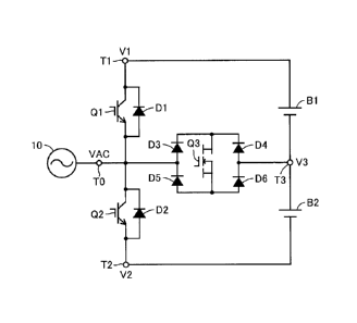
Fig. 1 is a circuit diagram showing a configuration of a converter according
to
Embodiment 1 of the present invention. With reference to Fig. 1, this
converter
includes an input terminal TO, output terminals T1 to T3 (first to third
output terminals),
diodes D1 to D6 (first to sixth diodes), and transistors Q1 to Q3 (first to
third
transistors).
Input terminal TO receives an AC voltage VAC of a commercial frequency from,
for example, a commercial AC power supply 10. Output terminals Ti and T3 are
connected respectively with the positive electrode and negative electrode of a
battery
Bl. Output terminals T3 and T2 are connected respectively with the
positive
electrode and negative electrode of a battery B2. Each of batteries B1 and B2
stores
DC power. Batteries B1 and B2 are charged with DC voltages having the same
value.
When the voltages at output terminals Ti, T2, and T3 are respectively DC
voltages V1, V2, and V3, V1 > V3 > V2, and V3 = (VI + V2)/2. This converter
converts AC voltage VAC applied to input terminal TO into DC voltages Vito V3
and
outputs DC voltages Vito V3 respectively to output terminals Ti to T3. If
output
terminal T3 is grounded, DC voltages Vito V3 are respectively a positive
voltage, a
negative voltage, and 0 V.
Diode Di has an anode connected to input terminal TO and a cathode connected
to output terminal TI. Diode D2 has an anode connected to output terminal 12
and a
cathode connected to input terminal TO. Transistor Q1 has a collector
connected to
output terminal T1 and an emitter connected to input terminal TO. Transistor
Q2 has a
collector connected to input terminal TO and an emitter connected to output
terminal T2.
Diodes D3 and D4 have anodes connected respectively to input terminal TO and
output terminal T3 and cathodes connected to each other. Diodes D5 and D6 have
- 4 -
84416308
cathodes connected respectively to input terminal TO and output terminal T3
and anodes
connected to each other.
Transistor Q3 has a drain (first electrode) connected to the cathodes of
diodes
D3 and D4 and a source (second electrode) connected to the anodes of diodes D5
and D6.
Diodes D3 to D6 and transistor Q3 constitute a first bidirectional switch
connected between
input terminal TO and output terminal T3.
Diode D1 allows a current to flow from input terminal TO to output terminal
Ti during a period in which AC voltage VAC is a positive voltage, thereby
charging battery
Bl. Diode D2 allows a current to flow from output terminal T2 to input
terminal TO during a
period in which AC voltage VAC is a negative voltage, thereby charging battery
B2.
Since diodes D1 and D2 allow flows of the currents that charge batteries B1
and B2, diodes D1 and D2 have rated currents set to relatively large values.
The rated current
of each of diodes D1 and D2 is, for example, 600 A, which is greater than the
rated current of
each of diodes D3 to D6 and transistors Q1 to Q3. For reduced loss in diodes
D1 and D2,
each of diodes D1 and D2 is made of silicon carbide (SiC) that is a wide
bandgap
semiconductor, which is, for example, a Schottky barrier diode.
In some cases, the power is regenerated from a load (not shown) such as a
motor connected with batteries B1 and B2, voltage V1 at output terminal Ti
exceeds a rated
voltage V1R, and voltage V2 at output terminal T2 falls below a rated voltage
V2R. Rated
voltage V1R is a voltage obtained by subtracting a threshold voltage of diode
D1 from a
positive peak voltage of AC voltage VAC. Rated voltage V2R is a voltage
obtained by
adding a threshold voltage of diode D2 to a negative peak voltage of AC
voltage VAC.
When voltage VI at output terminal Ti exceeds rated voltage V1R, transistor
Q1 allows a current to flow from output terminal Ti to input terminal TO, thus
reducing
voltage V1 at output terminal Ti. When voltage V2 at output terminal T2 falls
below rated
voltage V2R, transistor Q2 allows a current to flow from input terminal TO to
output terminal
T2, thus increasing voltage V2 at output terminal T2.
- 5 -
CA 3019875 2020-01-03
E11262W001: 9160013
CA 03019875 2018-10-03
Since this converter is used as a power conversion apparatus (e.g.,
uninterruptible power system) with small regenerated power, the rated currents
of
transistors Q1 and Q2 are set to relatively small values. The rated current of
each of
transistors Q1 and Q2 is, for example, 300 A, which is smaller than the rated
current of
each of diodes D1 to D6 and transistor Q3. Transistors Q1 and Q2 have a low
loss,
eliminating the need for forming transistors Q1 and Q2 using expensive wide
bandgap
semiconductors. Thus, for reduced device cost, each of transistors Q1 and Q2
is made
of silicon (Si) that is a semiconductor other than the wide bandgap
semiconductor,
which is, for example, an insulated gate bipolar transistor (IGBT).
Diodes D3 to D6 and transistor Q3 constitute a first bidirectional switch for
setting voltage V3 at output terminal T3 to an intermediate voltage between
voltages
V1 and V2 The rated current of each of diodes D3 to D6 and transistor Q3 is
set to a
value smaller than the rated current of each of diodes D1 and D2 and greater
than the
rated current of each of transistors Q1 and Q2. The rated current of each of
diodes D3
to D6 is, for example, 450 A. The rated current of transistor Q3 is, for
example, 500
A.
Diodes D3 to D6 have a low loss, thus eliminating the need for forming diodes
D3 to D6 using expensive wide bandgap semiconductors. For reduced device cost,
thus, each of diodes D3 to D6 is made of silicon (Si) that is a semiconductor
other than
the wide bandgap semiconductor. For a reduced loss of transistor Q3,
transistor Q3 is
made of silicon carbide (SiC) that is a wide bandgap semiconductor, which is,
for
example, an N-channel MOS transistor.
An operation of this converter will now be described. The gates of transistors
Q1 to Q3 are supplied respectively with pulse width modulation (PWM) signals
91 to
93 from a controller (not shown). Figs. 2 (a) to (d) show how PVVM signals 91
to 93
are generated and also the waveforms of these signals. In particular, Fig.
2(a) shows
the waveforms of a sine-wave command value signal CM, a positive-side
triangular
wave carrier signal CA1, and a negative-side triangular wave carrier signal
CA2, and
Figs. 2(b) to (d) respectively show the waveforms of PWM signals 92B, (p1B,
and 93.
- 6 -
E11262W001: 9160013
CA 03019875 2018-10-03
PWM signals 92B and 91B are respectively inversion signals of PWM signals 92
and
91.
With reference to Figs 2(a) to (d), the frequency of sine-wave command value
signal CM is, for example, a commercial frequency. The phase of sine-wave
command value signal CM is the same as, for example, the phase of AC voltage
VAC
of the commercial frequency. Carrier signals CA1 and CA2 have the same cycle
and
phase. The cycles of carrier signals CAI and CA2 are sufficiently smaller than
the
cycle of sine-wave command value signal CM.
The level of sine-wave command value signal CM is compared with the level of
positive-side triangular wave carrier signal CAl. When the level of sine-wave
command value signal CM is higher than the level of positive-side triangular
wave
carrier signal CAL PWM signal 91B is set to "L" level, and PWM signal 91 is
set to
"H" level. When the level of sine-wave command value signal CM is lower than
the
level of positive-side triangular wave carrier signal CAL PWM signal 91B is
set to "H"
level, and PVV11/1 signal 91 is set to "L" level.
Thus, PWM signal 91 is set to "H" level and "L" level in synchronization with
carrier signal CA1 during a period in which the level of sine-wave command
value
signal CM is positive, and PWM signal 91 is fixed to "L" level during a period
in
which the level of sine-wave command value signal CM is negative.
The ratio between the time in which the PWM signal is set to "H" level in one
cycle and the time of one cycle of the PWM signal is referred to as a duty
ratio.
During a period in which the level of sine-wave command value signal CM is
positive,
the duty ratio of PWM signal 91 is largest in the vicinity of a positive peak
(90 degrees)
of sine-wave command value signal CM, decreases as farther from the peak, and
is
smallest in the vicinity of 0 degrees and in the vicinity of 180 degrees.
During a
period in which the level of sine-wave command value signal CM is negative,
the duty
ratio of PWM signal 91 is fixed to 0.
The level of sine-wave command value signal CM is compared with the level of
negative-side triangular wave carrier signal CA2. When the level of sine-wave
- 7 -
E11262W001: 9160013
CA 03019875 2018-10-03
command value signal CM is higher than the level of negative-side triangular
wave
carrier signal CA2, PWM signal 92B is set to "H" level, and PWM signal qi2 is
set to
"L" level. When the level of sine-wave command value signal CM is lower than
the
level of negative-side triangular wave carrier signal CA2, PWM signal (p2B is
set to
"L" level, and PWM signal (p2 is set to "H" level.
During a period in which the level of sine-wave command value signal CM is
positive, thus, PWM signal (p2 is fixed to "L" level. During a period in which
the
level of sine-wave command value signal CM is negative, PWM signal (p2 is set
to "H"
level and "L" level in synchronization with carrier signal CA2. During a
period in
which the level of sine-wave command value signal CM is negative, the duty
ratio of
PWM signal cp2 is largest in the vicinity of a positive peak (270 degrees) of
sine-wave
command value signal CM, decreases as farther from the peak, and is smallest
in the
vicinity of 180 degrees and in the vicinity of 360 degrees. During a period in
which
the level of sine-wave command value signal CM is positive, the duty ratio of
PWM
signal cp2 is fixed to 0.
PWM signal cp3 is an AND signal of PWM signals cp2B and OB. PWM
signal cp3 is set to "H" level and "L" level in synchronization with carrier
signals CA1
and CA2. During a period in which the level of sine-wave command value signal
CM
is positive, the duty ratio of PWM signal (p3 is smallest in the vicinity of a
positive peak
(90 degrees) of sine-wave command value signal CM, increases as farther from
the
peak, and is largest in the vicinity of 0 degrees and in the vicinity of 180
degrees.
During a period in which the level of sine-wave command value signal CM is
negative,
the duty ratio of PWM signal (p3 is smallest in the vicinity of a negative
peak (270
degrees) of sine-wave command value signal CM, increases as farther from the
peak,
and is largest in the vicinity of 180 degrees and in the vicinity of 360
degrees.
A current flowing through each of diodes DI to D6 and transistors Q1 to Q3
during the operation of the converter will now be described. It is assumed
that the
power factor is 1.0 and that sine-wave command value signal CM and AC voltage
VAC
match in phase. During a period in which the level of sine-wave command value
- 8 -
E11262W001: 9160013
CA 03019875 2018-10-03
signal CM is positive, PWM signals 91 and 93 are alternately set to "H" level,
and
PWM signal 92 is fixed to "L" level.
During this period, when DC voltage VI is lower than rated voltage V1R, and
when PWM signals 91 and 93 are set respectively to "H" level and "L" level,
transistor
Q3 is turned off and a current Ii at a level that corresponds to the level of
AC voltage
VAC flows from input terminal TO via diode D1 to output terminal Tl. At this
time,
no current flows through transistor Ql.
During this period, when the power is regenerated from the load (not shown) to
battery B1 and DC voltage V1 exceeds rated voltage V1R, and when PWM signals
91
and 93 are set respectively to "H" level and "L" level, transistor Q1 is
turned on and
transistor Q3 is turned off. This allows a current Ti at a level that
corresponds to the
levels of DC voltage V1 and AC voltage VAC to flow from output terminal Ti via
transistor Q1 to input terminal TO, so that DC voltage V1 decreases to rated
voltage
V1R.
When PWM signals 91 and 93 are set respectively to "L'' level and "H" level,
transistor Q1 is turned off and transistor Q3 is turned on, allowing a current
HA at a
level that complements current Ii to flow through a path from input terminal
TO via
diode D3, transistor Q3, and diode D6 to output terminal T3.
During this period, the effective value of the current flowing through diode
D1
is largest among diodes D1 to D6 and transistors Q1 to Q3, and a switching
loss occurs
in transistor Q3. A reverse bias voltage is applied to diode D1 every time
transistor
Q3 changes from on state to off state, so that diode D1 performs a reverse
recovery
operation. During this period, no current flows through diodes D2, D4, and D5.
Since DC voltage VI exceeds rated voltage V1R for a short period of time, a
low loss
occurs in transistor Ql.
During a period in which the level of sine-wave command value signal CM is
negative, PWM signals 92 and 93 are alternately set to "H" level, and PWM
signal 91
is fixed to "L" level. During this period, when DC voltage V2 is higher than
rated
voltage V2R, and when PWM signals 92 and 93 are set respectively to "H" level
and
- 9 -
E11262W001: 9160013
CA 03019875 2018-10-03
"L" level, transistor Q3 is turned off, allowing a current 12 at a level that
corresponds to
the levels of DC voltage V2 and AC voltage VAC to flow from output terminal T2
via
diode D2 to input terminal TO. At this time, no current flows through
transistor Q2.
Rated voltage V2R is a voltage that is a difference between the negative-side
peak
value of AC voltage VAC and the threshold voltage of diode D2.
During this period, when, for example, the power is regenerated from the load
(not shown) to battery B2 and DC voltage V2 falls below rated voltage V2R, and
when
PWM signals 92 and 93 are set respectively to "H" level and "L" level,
transistor Q2 is
turned on and transistor Q3 is turned off This allows a current 12 at the
level that
corresponds to the levels of DC voltage V2 and AC voltage VAC to flow from
input
terminal TO via transistor Q2 to output terminal T2, so that DC voltage V2
increases to
rated voltage V2R.
When PWM signals 92 and 93 are set respectively to "L" level and "H" level,
transistor Q2 is turned off and transistor Q3 is turned on, allowing a current
12A at a
level that complements a current 12 to flow through a path from output
terminal T3 via
diode D4, transistor Q3, and diode D5 to input terminal TO.
During this period, the effective value of the current flowing through diode
D2
is largest among diodes D1 to D6 and transistors Q1 to Q3, and a switching
loss occurs
in transistor Q3. A reverse bias voltage is applied to diode D2 every time
transistor
Q3 changes from off state to on state, so that diode D2 performs the reverse
recovery
operation. During this period, no current flows through diodes DI, D3, and D6.
Since DC voltage V2 falls below rated voltage V2R in a short period of time,
the loss
generated in transistor Q2 is low.
In summary, a large current flows through diodes D1 and D2, so that diodes D1
and D2 perform the reverse recovery operation. A current smaller than the
current
through diodes D1 and D2 flows through diodes D3 to D6, so that diodes D3 to
D6 do
not perform the reverse recovery operation. A current flows through transistor
Q3,
and a switching loss occurs in transistor Q3. A current flows through
transistors Q1
and Q2 in a short period of time, and losses that occur in transistors Q1 and
Q2 are low.
- 10 -
E11262W001: 9160013
CA 03019875 2018-10-03
Thus, Schottky barrier diodes that are made of SiC being a wide bandgap
semiconductor and have a rated current of a large value (e.g., 600 A) are used
as diodes
DI and D2 as described, thereby reducing a recovery loss during the reverse
recovery
operation. Diodes that are made of Si being a semiconductor other than the
wide
bandgap semiconductor and have a rated current of a small value (e.g., 450 A)
are used
as diodes D3 to D6, thereby reducing cost.
Further, an N-channel MOS transistor that is made of SiC being a wide bandgap
semiconductor and has a rated current of a large value (e.g., 500 A) is used
as transistor
Q3, thus reducing a switching loss. IGBTs that are made of Si being a
semiconductor
other than a wide bandgap semiconductor and have a rated current of a small
value (e.g.,
450 A) are used as transistors Q1 and Q2, thereby reducing cost.
Fig 3(a) is a time chart showing a switching operation of an N-channel MOS
transistor (referred to as a Si transistor) made of Si, and Fig. 3(b) is a
time chart
showing a switching operation of an N-channel MOS transistor (referred to as a
SiC
transistor) made of SiC.
With reference to Figs. 3(a) and (b), it is assumed that in the initial state,
a gate
signal (not shown) is set to "H" level to turn on the transistor, a constant
current I flows
through the transistor, and a drain-source voltage Vds is 0 V. When the gate
signal is
lowered from "H'' level to "L" level to turn off the transistor at a certain
time, current I
decreases and voltage Vds increases.
As can be seen from Figs. 3(a) and (b), a time Ta taken for current I to start
dropping to reach 0 A in the Si transistor is longer than a time Tb taken for
current Ito
start dropping to reach 0 A in the SiC transistor. In the Si transistor,
current I
decreases rapidly down to a certain value but changes from the certain value
to 0 A for
a longer period of time. The current flowing while changing from a certain
value to 0
A is referred to as a tail current.
In the SiC transistor, contrastingly, current I decreases rapidly, and a
slight
overshoot occurs. The switching loss of a transistor, which is the product of
current I
and voltage Vds, corresponds to the area of a hatched portion in the drawing.
The
- 11 -
E11262W001: 9160013
CA 03019875 2018-10-03
switching loss of the SiC transistor is thus lower than the switching loss of
the Si
transistor.
Fig. 4 shows the appearance of the converter shown in Fig. 1. With reference
to Fig. 4, the converter includes one semiconductor module Ml. Semiconductor
module MI is internally provided with diodes DI to D4 and transistors Q1 to
Q3.
Semiconductor module MI is externally provided with input terminal TO and
output
terminals Ti to T3. Although semiconductor module MI is externally provided
with
signal terminals for supplying PWM signals 91 to 93 to the gates of
transistors Ql to
Q3, the signal terminals are not shown for simplicity of the drawing.
Fig. 5 is a circuit block diagram showing a configuration of an
uninterruptible
power system including the converter shown in Fig. I. With reference to Fig.
5, the
uninterruptible power system includes an input filter 1, a converter 2, a DC
positive bus
L I , a DC negative bus L2, a DC neutral point bus L3, capacitors Cl and C2,
an inverter
3, an output filter 4, and a controller 5.
Input filter I, which is a low pass filter, allows the AC power of a
commercial
frequency from commercial AC power supply 10 to pass through input terminal TO
of
converter 2 and also prevents a signal of a carrier frequency generated in
converter 2
from passing toward commercial AC power supply 10.
DC positive bus Li, DC negative bus L2, and DC neutral point bus L3 have
first terminals connected respectively to output terminals T1, T2, and T3 of
converter 2,
and second terminals connected to three respective input terminals of inverter
3.
Capacitor Cl is connected between buses Li and L3, and capacitor C2 is
connected
between buses L3 and L2. Buses Li and L3 are connected respectively to the
positive
electrode and negative electrode of battery B I, and buses L3 and L2 are
connected
respectively to the positive electrode and negative electrode of battery B2.
As shown in Fig. 1, converter 2 includes input terminal TO, output terminals
T1
to T3, diodes D1 to D6, and transistors Q1 to Q3 and is controlled by PWIVI
signals 91
to 93 from controller 5.
During a normal operation in which AC power is supplied normally from
- 12 -
E11262W001: 9160013
CA 03019875 2018-10-03
commercial AC power supply 10, converter 2 converts AC power supplied from
commercial AC power supply 10 via input filter 1 into DC power and supplies
the DC
power to each of batteries B1 and B2 and also to inverter 3. Each of batteries
B1 and
B2 stores the DC power.
In other words, converter 2 is controlled by PWM signals cp1 to 93 supplied
from controller 5, generates DC voltages Vito V3 based on AC voltage VAC
supplied
from commercial AC power supply 10 via input filter 1, and supplies DC
voltages V1
to V3 generated respectively to DC positive bus LI, DC negative bus L2, and DC
neutral point bus L3. If output terminal T3 is grounded, DC voltages Vito V3
are
respectively a positive voltage, a negative voltage, and 0 V. DC voltages Vito
V3
are smoothed by capacitors Cl and C2. DC voltages Vito V3 are supplied to
batteries B1 and B2 and inverter 3. During a power failure in which a supply
of AC
power from commercial AC power supply 10 is stopped, transistor Q1 is fixed to
off
state, so that the operation of converter 2 is stopped.
Inverter 3 converts DC power generated in converter 2 into AC power during a
normal operation in which commercial AC power supply 10 supplies AC power
normally and converts DC power of batteries B1 and B2 into AC power during a
power
failure in which a supply of AC power from commercial AC power supply 10 is
stopped.
In other words, inverter 3 generates an AC voltage at three levels based on DC
voltages Vito V3 supplied from converter 2 via buses Li to L3 during a normal
operation and generates AC voltage at three levels based on DC voltages Vito
V3
supplied from batteries B1 and B2 via buses Li to L3 during a power failure.
Output filter 4 is connected between the output terminal of inverter 3 and
load
11. Output filter 4, which is a low pass filter, allows the AC power having a
commercial frequency of the AC power output from inverter 3 to pass through
load 11
and prevents a signal having a carrier frequency which is generated in
inverter 3 from
passing toward load 11. In other words, output filter 4 converts the output
voltage of
inverter 3 into a sine wave of a commercial frequency and supplies the sine
wave to
- 13 -
El 1262W001: 9160013
CA 03019875 2018-10-03
load 11.
Controller 5 controls converter 2 and inverter 3 by supplying a PWM signal
while monitoring, for example, the AC voltage from commercial AC power supply
10,
the AC voltage output to load 11, and DC voltages Vito V3.
The operation of this uninterruptible power system will now be described.
During a normal operation in which commercial AC power supply 10 supplies AC
power normally, the AC power from commercial AC power supply 10 is supplied to
converter 2 via input filter 1 and is converted into DC power by converter 2.
The DC
power generated in converter 2 is stored in batteries B1 and B2 and is also
supplied to
inverter 3, and is then converted into AC power of a commercial frequency by
inverter
3. The AC power generated in inverter 3 is supplied to load 11 via
output filter 4,
thereby operating load 11.
At the occurrence of regenerated power in load 11, the regenerated power is
returned to commercial AC power supply 10 via output filter 4, inverter 3,
buses Li to
L3, converter 2, and input filter 1.
During a power failure in which a supply of AC power from commercial AC
power supply 10 is stopped, the operation of converter 2 is stopped, and the
DC power
of batteries Bl and B2 is supplied to inverter 3 and is then converted into AC
power of
a commercial frequency by inverter 3. The AC power generated in inverter 3 is
supplied to load 11 via output filter 4, so that the operation of load 11 is
continued.
Even when a power failure occurs, thus, the operation of load 11 is continued
as
long as batteries B1 and B2 store DC power. Upon restart of a supply of the AC
power from commercial AC power supply 10, converter 2 restarts the operation,
and
the DC power generated in converter 2 is supplied to batteries B1 and B2 and
inverter 3,
returning to the original state.
As described above, since a converter is composed of three transistors Q1 to
Q3
and six diodes D1 to D6, fewer semiconductor elements can be used than in a
conventional case, thereby reducing the size and cost of the device. Besides,
since
diodes D1 and D2 that perform the reverse recovery operation and transistor Q3
that
- 14 -
E11262W001: 9160013
CA 03019875 2018-10-03
switches a current are made of wide bandgap semiconductors, a recovery loss
and a
switching loss can be reduced. Further, since diodes D3 to D6 that do not
perform the
reverse recovery operation and transistors Q1 and Q2 that allow a current to
flow
during only the regeneration operation are made of semiconductors other than
wide
bandgap semiconductors, thereby reducing cost.
Although SiC is used as the wide bandgap semiconductor in Embodiment 1, the
present invention is not limited to this. Other semiconductors can be used as
long as
they are wide bandgap semiconductors. For example, gallium nitride (GaN) can
be
used as the wide bandgap semiconductor.
[Embodiment 2]
Fig. 6 is a circuit block diagram showing a configuration of inverter 3 of an
uninterruptible power system according to Embodiment 2 of the present
invention.
The general arrangement of the uninterruptible power system is as shown in
Fig. 5.
Converter 2 of the uninterruptible power system is the converter shown in Fig.
1.
With reference to Fig. 6, inverter 3 includes input terminals T11 to T13
(first to third
output terminals), an output terminal T14 (fourth output terminal),
transistors Q11 to
Q14 (fourth to seventh transistors), and diodes Dll to D14 (seventh to tenth
diodes).
Input terminals T11 to T13 are connected respectively to DC positive bus Li,
DC negative bus L2, and DC neutral point bus L3 of Fig. 5. Input terminals T11
and
T13 are connected respectively with the positive electrode and negative
electrode of
battery Bl. Input terminals T13 and T12 are connected respectively with the
positive
electrode and negative electrode of battery B2. Each of batteries B1 and B2
outputs
DC voltage. The output voltage of battery B1 is equal to the output voltage of
battery
B2. Thus, DC voltages V1, V2, and V3 are applied respectively to input
terminals
T11, 112, and T13, and V1 > V3 > V2 and V3 = (V1 + V2)/2. This inverter
converts
DC voltages Vito V3 applied to input terminals T11 to T13 into an AC voltage
V4 at
three levels and then outputs AC voltage V4 to output terminal T14. If input
terminal
T13 is grounded, DC voltages Vito V3 are respectively a positive voltage, a
negative
voltage, and 0 V.
- 15 -
E11262W001: 9160013
CA 03019875 2018-10-03
Each of transistors Q11 and Q12 is made of silicon carbide (SiC) that is a
wide
bandgap semiconductor, which is an N-channel MOS transistor, for example. The
rated current of each of transistors Q11 and Q12 is, for example, 600 A and is
greater
than the rated current of each of transistors Q13 and Q14 and diodes Dll to
D14.
Each of transistors Q13 and Q14 is made of silicon (Si) that is a
semiconductor
other than a wide bandgap semiconductor, which is an IGBT, for example. The
rated
current of each of transistors Q13 and Q14 is 450 A, for example.
Each of diodes Dll and D12 is made of silicon (Si) made of a semiconductor
other than a wide bandgap semiconductor. The rated current of each of diodes
Dll
and D12 is 300 A, for example.
Each of diodes D13 and D14 is a Schottky barrier diode made of silicon carbide
(SiC) that is a wide bandgap semiconductor. The rated current of each of
diodes D13
and D14 is 500 A, for example. The rated current of each of transistors Q11
and Q12
is greater than the rated current of each of transistors Q13 and Q14 and
diodes Dll to
D14.
The reason why the specifications of transistors Q11 and Q12 differ from the
specifications of transistors Q13 and Q14 and the specifications of diodes Dll
and D12
differ from the specifications of diodes D13 and D14 will be described below.
Transistor Q11 has a drain (first electrode) connected to input terminal T11
and
a source (second electrode) connected to output terminal T14. Diode D11 has an
anode connected to output terminal T14 and a cathode connected to input
terminal T11.
Transistor Q12 has a drain connected to output terminal T14 and a source
connected to input terminal T12 Diode D12 has an anode connected to input
terminal
T12 and a cathode connected to output terminal T14 That is to say, diodes Dll
and
D12 are connected respectively in anti-parallel with transistors Q11 and Q12.
Transistors Q13 and Q14 have collectors (first electrodes) connected to each
other and emitters (second electrodes) connected respectively to input
terminal T13 and
output terminal T14. Diodes D13 and D14 have cathodes connected together to
the
collectors of transistors Q13 and Q14 and anodes connected respectively to
input
- 16-
E11262W001: 9160013
CA 03019875 2018-10-03
terminal T13 and output terminal T14. That is to say, diodes D13 and D14
are
connected respectively in anti-parallel with transistors Q13 and Q14.
Transistors Q13
and Q14 and diodes D13 and D14 constitute a second bidirectional switch
connected
between input terminal T13 and output terminal T14.
The operation of this inverter will now be described. The gates of transistors
Q11 to Q14 are supplied respectively with PWM signals 911 to 914 from
controller 5.
Figs. 7(a) to (e) show how PWM signals 911 to 914 are generated and the
waveforms
of these signals. In particular, Fig. 7(a) shows the waveforms of sine-wave
command
value signal CM, positive-side triangular wave carrier signal CA], and
negative-side
triangular wave carrier signal CA2, and Figs. 7(b) to (e) respectively show
the
waveforms of PWM signals 911, 914, 913, and 912.
With reference to Figs. 7(a) to (e), the frequency of sine-wave command value
signal CM is, for example, a commercial frequency. Carrier signals CA1 and CA2
have the same cycle and phase. The cycles of carrier signals CA1 and CA2 are
sufficiently smaller than the cycle of sine-wave command value signal CM.
The level of sine-wave command value signal CM is compared with the level of
positive-side triangular wave carrier signal CAL When the level of sine-wave
command value signal CM is higher than the level of positive-side triangular
wave
carrier signal CA1, PWM signals 911 and 913 are set respectively to "H" level
and "L"
level. When the level of sine-wave command value signal CM is lower than the
level
of positive-side triangular wave carrier signal CA1, PWM signals 911 and 913
are set
respectively to "L" level and "H" level.
During a period in which the level of sine-wave command value signal CM is
positive, thus, PWM signals 911 and 913 are alternately set to "H" level in
synchronization with carrier signal CA1, so that transistors Q11 and Q13 are
alternately
turned on. During a period in which the level of sine-wave command value
signal
CM is negative, PWM signals 911 and 913 are set respectively to "L" level and
"H"
level, and the transistor Q11 is fixed to off state and transistor Q13 is
fixed to on state.
The level of sine-wave command value signal CM is compared with the level of
- 17 -
E11262W001: 9160013
CA 03019875 2018-10-03
negative-side triangular wave carrier signal CA2. When the level of sine-wave
command value signal CM is higher than the level of negative-side triangular
wave
carrier signal CA2, PWM signals 912 and 914 are set respectively to "L" level
and "H"
level. When the level of sine-wave command value signal CM is lower than the
level
of negative-side triangular wave carrier signal CA2, PWM signals 912 and 914
are set
respectively to "H" level and "L" level.
During a period in which the level of sine-wave command value signal CM is
positive, thus, PWM signals 912 and 914 are set respectively to "L" level and
"H" level,
and transistor Q12 is fixed to off state and transistor Q14 is fixed to on
state. During a
period in which the level of sine-wave command value signal CM is negative,
PWM
signals 912 and 914 are alternately set to "H" level in synchronization with
carrier
signal CA2, so that transistors Q12 and Q14 are alternately turned on.
The ratio between the time in which the PWM signal is set to "H" level in one
cycle and the time of one cycle of the PWM signal is referred to as a duty
ratio.
During a period in which the level of sine-wave command value signal CM is
positive,
the duty ratio of PWM signal 911 is largest in the vicinity of a positive peak
(90
degrees) of sine-wave command value signal CM, decreases as farther from the
peak,
and is zero in the vicinity of 0 degrees and in the vicinity of 180 degrees.
The duty
ratio of PWM signal 911 is fixed to zero during a period in which the level of
sine-
wave command value signal CM is negative. PWM signal 913 is an inversion
signal
of PWM signal 911.
The duty ratio of PWM signal 912 is fixed to zero during a period in which the
level of sine-wave command value signal CM is positive. The duty ratio of PWM
signal 912 is largest in the vicinity of a negative peak (270 degrees) of sine-
wave
command value signal CM, decreases as farther from the peak, and is zero in
the
vicinity of 180 degrees and in the vicinity of 360 degrees. The duty ratio of
PWM
signal 912 is fixed to zero during a period in which the level of sine-wave
command
value signal CM is positive. PWM signal 914 is an inversion signal of PWM
signal
912.
- 18 -
E11262W001: 9160013
CA 03019875 2018-10-03
The current flowing through each of transistors Q11 to Q14 and diodes Dll to
D14 during the operation of the inverter will now be described. It is assumed
as
shown in Fig. 8 that the current flowing from input terminal T11 to output
terminal T14
is 11 1, the current flowing from output terminal T14 to input terminal T12 is
112, the
current flowing from input terminal T13 to output terminal T14 is 113, and the
current
flowing from output terminal T14 to input terminal T13 is 114.
Figs. 9(a) to (i) are time charts showing the operation of the inverter. In
particular, Fig. 9(a) shows the waveforms of sine-wave command value signal
CM,
positive-side triangular wave carrier signal CA1, and negative-side triangular
wave
carrier signal CA2, Figs. 9(b), (d), (f), and (h) respectively show the
waveforms of
PWM signals 911, 914, 913, and 912, and Figs_ 9(c), (e), (g), and (i)
respectively show
the waveforms of currents Iii, 114, 113, and 112. The positive currents of
currents Ill
to 114 show the currents flowing through transistor Q, and the negative
currents thereof
show the currents flowing through diode D. Shown here is the case in which the
power factor is 1Ø
With reference to Figs. 9(a) to (i), during a period in which the level of
sine-
wave command value signal CM is positive, PWM signals 9 1 4 and 9 1 2 are
fixed
respectively to "H" level and "L" level, and PWM signals 911 and 913 are
alternately
set to "H" level. Thus, transistors Q14 and Q12 are fixed respectively to on
state and
off state, so that transistors Q11 and Q13 are alternately turned on and DC
voltages V1
and V3 alternately appear at output terminal T14.
During this period, current Iii at the level that corresponds to on time of
transistor Q11 flows when transistor Q11 is turned on, and current 113 at the
level that
complements current Iii flows through a path formed of diode D13 and
transistor Q14
when transistor Q11 is turned off
Since transistor Q12 is fixed to off state, no current flows through
transistor
Q12, and no switching loss occurs in transistor Q12. Since a current flows
through
diode D13 and no current flows through transistor Q13 though transistor Q13 is
turned
on/off, no switching loss occurs in transistor Q13. Since transistor Q14 is
fixed to on
- 19 -
El 1262W001: 9160013
CA 03019875 2018-10-03
state, a current flows through transistor Q14, but no switching loss occurs in
transistor
Q14. During this period, thus, the effective value of the current flowing
through
transistor Q11 is largest and the switching loss in transistor Q11 is largest
among
transistors Q11 to Q14.
A reverse bias voltage is applied to diode D13 every time transistor Q11
changes from off state to on state, so that diode D13 performs the reverse
recovery
operation. During this period, no current flows through diodes D11, D12, and
D14.
During a period in which the level of sine-wave command value signal CM is
negative, PWM signals p13 and p11 are fixed respectively to "H" level and "L"
level,
and PWM signals cp12 and 914 are alternately set to "H" level. Thus,
transistors Q13
and Q11 are fixed respectively to on state and off state, and transistors Q12
and Q14
are alternately turned on, so that DC voltages V2 and V3 alternately appear at
output
terminal T14.
During this period, current 112 at the level that corresponds to on time of
transistor Q12 flows when transistor Q12 is turned on, and current 113 flows
through a
path formed of diode D14 and transistor Q13 when transistor Q12 is turned off.
Since transistor Q11 is fixed to off state, no current flows through
transistor
Q11, and no switching loss occurs in transistor Q11. Since a current flows
through
diode D14 and no current flows through transistor Q14 though transistor Q14 is
turned
on/off, no switching loss occurs in transistor Q14. Since transistor Q13 is
fixed to on
state, a current flows through transistor Q13 but no switching loss occurs in
transistor
Q13. During this period, thus, the effective value of the current flowing
through
transistor Q12 is largest and the switching loss in transistor Q12 is largest
among
transistors Q11 to Q14.
A reverse bias voltage is applied to diode D14 every time transistor Q12
changes from off state to on state, so that diode D14 performs the reverse
recovery
operation. During this period, no current flow through diodes Dll, D12, and
D13.
In summary, a large current flows through transistors Q11 and Q12, and a
switching loss occurs in transistors Q11 and Q12. A current smaller than the
current
- 20 -
E11262W001: 9160013
CA 03019875 2018-10-03
through transistors Q11 and Q12 flows through transistors Q13 and Q14, and no
switching loss occurs in transistors Q13 and Q14.
N-channel MOS transistors that are made of SiC being a wide bandgap
semiconductor and have a rated current of a large value (e.g., 600 A) are used
as
transistors Q11 and Q12 as described above, thereby reducing switching loss.
IGBTs
that are made of Si being a semiconductor other than the wide bandgap
semiconductor
and have a rated current of a small value (e.g., 450 A) are used as
transistors Q13 and
Q14, thereby reducing cost.
A current equivalent to the current through transistors Q13 and Q14 flows
through diodes D13 and D14, so that diodes D13 and D14 perform the reverse
recovery
operation. No current flows through diodes D1 1 and D12. As is commonly known,
diodes Dll and D12 are provided to protect transistors Q11 and Q12 from a
voltage
generated in an inductor when the inductor is used as the load.
Thus, Schottky barrier diodes that are made of SiC being a wide bandgap
semiconductor and have a rated current of a value (e.g., 500A) equivalent to
that of
transistors Q13 and Q14 are used as diodes D13 and D14 as described above,
thereby
reducing recovery loss during the reverse recovery operation. Diodes that are
made of
Si being a semiconductor other than the wide bandgap semiconductor and have a
rated
current of a small value (e.g., 300 A) are used as diodes Dll and D12, thereby
reducing
cost.
Fig. 10 shows the appearance of inverter 3 shown in Fig. 6. With reference to
Fig. 10, inverter 3 includes one semiconductor module M2. Semiconductor module
M2 is internally provided with transistors Q11 to Q14 and diodes Dll to D14.
Semiconductor module M2 is externally provided with input terminals T11 to T13
and
output terminal T14. Further, although semiconductor module M2 is externally
provided with four signal terminals for supplying PWM signals cp11 to (p14 to
the gates
of transistors Q11 to Q14, the four terminals are not shown for simplicity of
the
drawing.
As described above, N-channel MOS transistors made of wide bandgap
- 21 -
E11262W001: 9160013
CA 03019875 2018-10-03
semiconductors are used as transistors Q11 and Q12 that turn on/off current
and IGBTs
made of semiconductors other than wide bandgap semiconductors are used as
transistors Q13 and Q14 that do not turn on/off current in Embodiment 2, thus
reducing
switching loss and cost.
Further, Schottky barrier diodes made of wide bandgap semiconductors are used
as diodes D13 and D14 that perform the reverse recovery operation and diodes
made of
semiconductors other than wide bandgap semiconductors are used as diodes D11
and
D12 that do not perform the reverse recovery operation, thus reducing the
recovery loss
and cost.
Although SiC is used as a wide bandgap semiconductor in Embodiment 2, the
present invention is not limited to this. Any other semiconductor can be used
as long
as it is a wide bandgap semiconductor. For example, gallium nitride (GaN) can
be
used as the wide bandgap semiconductor.
[Embodiment 3]
Fig. 11 is a circuit diagram showing a configuration of an inverter of an
uninterruptible power system according to Embodiment 3 of the present
invention,
which is compared with Fig. 6. With reference to Fig. 11, this inverter
differs from
inverter 3 of Fig. 6 in that the parallel connection structure of transistor
Q13 and diode
D13 and the parallel connection structure of transistor Q14 and diode D14 are
replaced.
Transistors Q13 and Q14 have emitters connected to each other and collectors
connected respectively to input terminal T13 and output terminal T14.
Transistors
Q11 to Q14 are controlled respectively by PWM signals 911 to 914. When DC
voltages V1 and V3 are alternately output to output terminal T14, transistor
Q14 is
turned on and transistors Q11 and Q13 are alternately turned on. When DC
voltages
V2 and V3 are alternately output to output terminal T14, transistor Q13 is
turned on
and transistors Q12 and Q14 are alternately turned on.
Since the other configuration and operation are the same as those of
Embodiment 2, description thereof will not be repeated. Embodiment 3 also
achieves
the same effects as those of Embodiment 2.
- 22 -
CA 03019875 2018-10-03
E11262W001: 9160013
[Embodiment 4]
Fig. 12 is a circuit diagram showing a configuration of an inverter of an
uninterruptible power system according to Embodiment 4 of the present
invention,
which is compared with Fig. 6. With reference to Fig. 12, this inverter
differs from
inverter 3 of Fig. 6 in that the collectors of transistors Q13 and Q14 are
isolated from
the cathodes of diodes D13 and D14, the collector of transistor Q13 and the
cathode of
diode D14 are connected, and the collector of transistor Q14 and the cathode
of diode
D13 are connected.
Transistors Q11 to Q14 are controlled respectively by PWM signals 911 to 914.
When DC voltages V1 and V3 are alternately output to output terminal T14,
transistor
Q14 is turned on and transistors Q11 and Q13 are alternately turned on. When
DC
voltages V2 and V3 are alternately output to output terminal T14, transistor
Q13 is
turned on and transistors Q12 and Q14 are alternately turned on.
Since the other configuration and operation are the same as those of
Embodiment 2, description thereof will not be repeated. Embodiment 4 also
achieves
the same effects as those of Embodiment 2.
[Embodiment 5]
Fig. 13 is a circuit block diagram showing a configuration of an
uninterruptible
power system according to Embodiment 5 of the present invention. Fig. 14 is a
circuit
diagram showing configurations of a converter 22 and an inverter 24 shown in
Fig. 13.
Fig. 15 is a circuit diagram showing a configuration of a bidirectional
chopper 23
shown in Fig. 13. With reference to Figs. 13 to 15, the uninterruptible power
system
includes an input filter 21, converter 22, a DC positive bus Li, a DC negative
bus L2, a
DC neutral point bus L3, capacitors Cl and C2, bidirectional chopper 23,
inverter 24,
and an output filter 25. For simplicity of the drawing, a controller that
controls
converter 22, bidirectional chopper 23, and inverter 24 will not be shown.
Input filter 21 includes reactors 31 to 33 and capacitors 34 to 36. Reactors
31
to 33 have first terminals that respectively receive three-phase AC voltages
VU, VV,
and VW from commercial AC power supply 20 and second terminals connected
- 23 -
El 1262W001: 9160013
CA 03019875 2018-10-03
respectively to input terminals TOa to TOc of converter 22. Capacitors 34 to
36 have
first electrodes connected respectively to the first terminals of reactors 31
to 33 and
second electrodes connected together to neutral point NP. Reactors 31 to 33
and
capacitors 34 to 36 constitute a low pass filter. Input filter 21 allows the
three-phase
AC power of a commercial frequency from commercial AC power supply 20 to pass
through converter 22 and also prevents a signal of a carrier frequency
generated in
converter 22 from passing toward commercial AC power supply 20.
DC positive bus Li, DC negative bus L2, and DC neutral point bus L3 have
first terminals connected respectively to output terminals TI, T2, and T3 of
converter
22 and second terminals connected respectively to input terminals T11, T12,
and T13
of inverter 24 Capacitor Cl is connected between buses Li and L3, and
capacitor C2
is connected between buses L3 and L2. Buses Li to L3 are connected to battery
B11
via bidirectional chopper 23.
As shown in Fig. 14, converter 22 includes input terminals TOa to TOc, output
terminals Ti to T3, diodes Dla to Dlc and D2a to D2c, transistors Qla to Q1c
and Q2a
to Q2c, and bidirectional switches Sla to Sic. Input terminals TOa to TOc
respectively receive three-phase AC voltages VU, VV, and VW supplied from
commercial AC power supply 20 via input filter 21.
Diodes Dla to Dlc have anodes connected respectively to input terminals TOa
to TOc and cathodes connected together to output terminal Ti. Diodes D2a to
D2c
have anodes connected together to output terminal T2 and cathodes connected
respectively to input terminals TOa to TOc.
Transistors Qla to Qlc have collectors connected together to output terminal
Ti
and emitters connected respectively to input terminals TOa to TOc. Transistors
Q2a to
Q2c have collectors connected respectively to input terminals TOa to TOc and
emitters
connected together to output terminal T2.
Transistors Qla to Qlc are connected respectively by PWM signals p I a, cp lb,
and (plc from the controller (not shown). The waveforms of PWM signals pi a,
(plb,
and plc are similar to the waveform of the inversion signal of PWM signal 91B
shown
- 24 -
E11262W001: 9160013
CA 03019875 2018-10-03
in Fig. 2(c). The phases of PWM signals (p la, (p lb, and (plc are
synchronized
respectively with the phases of three-phase AC voltages VU, VV, and VW, and
are
shifted from each other by 120 degrees.
Transistors Q2a to Q2c are controlled respectively by PWM signals (p2a, (p2b,
and (p2c from the controller (not shown). The waveforms of PWM signals (p2a,
(p2b,
and (p2c are similar to the waveform of the inversion signal of PWM signal
(p2B shown
in Fig. 2(b). The phases of PWM signals (p2a, (p2b, and (p2c are synchronized
respectively with the phases of three-phase AC voltages VU, VV, and VW and are
shifted from each other by 120 degrees.
Bidirectional switches Sla to Sic have first terminals connected respectively
to
input terminals TOa to TOc and second terminals connected together to output
terminal
T3. Each of bidirectional switches Sla to Sic includes diodes D3 to D6
and N-
channel MOS transistor Q3 as shown in Fig. 1.
The anode of diode D3 and the cathode of diode D5 are connected together to
input terminal TOa (or TOb or T0c). The anode of diode D4 and the cathode of
diode
D6 are connected together to output terminal T3. The cathodes of diodes D3 and
D4
are connected to each other, and the anodes of diodes D5 and D6 are connected
to each
other. The drain of transistor Q3 is connected to the cathodes of diodes D3
and D4,
and the source of transistor Q3 is connected to the anodes of diodes D5 and
D6.
Transistors Q3 of bidirectional switches Sla to Sic are controlled
respectively
by PWM signals (p3a, (p3b, and (p3c from the controller (not shown). The
waveforms
of PWM signals 93a, (p3b, and (p3c are similar to the waveform of PWM signal
(p3
shown in Fig. 2(d). The phases of PWM signals 93a, (p3b, and (p3c are
synchronized
respectively with the phases of three-phase AC voltages VU, VV, and VW and are
shifted from each other by 120 degrees.
That is to say, input terminal T0a, output terminals Ti to T3, diodes Dla and
D2a, transistors Qla and Q2a, and bidirectional switch Sla constitute the
converter
shown in Fig. 1, and the converter converts AC voltage VU into DC voltages
Vito V3
and outputs these DC voltages to output terminals Ti to T3. Input terminal
TOb,
- 25 -
E11262W001: 9160013
CA 03019875 2018-10-03
output terminals Ti to 13, diodes D lb and D2b, transistors Q lb and Q2b, and
bidirectional switch Sib constitute the converter shown in Fig. 1, and the
converter
converts AC voltage VV into DC voltages Vito V3 and outputs these DC voltages
to
output terminals Ti to T3.
Input terminal TOc, output terminals Ti to 13, diodes Die and D2c, transistors
Qlc and Q2c, and bidirectional switch Sic constitute the converter shown in
Fig. 1, and
the converter converts AC voltage VW into DC voltages Vito V3 and outputs
these
DC voltages to output terminals Ti to 13. Converter 22 converts three-phase AC
voltages VU, VV, and VW into DC voltages Vito V3 and outputs these DC voltages
to output terminals Ti to T3.
As described in Embodiment 1, diodes Dla to Die and D2a to D2c and
transistors Q3 of bidirectional switches Sla to Sic are made of wide bandgap
semiconductors, and transistors Qla to Qlc and Q2a to Q2c and diodes D3 to D6
of
bidirectional switches Sla to Sic are made of semiconductors other than the
wide
bandgap semiconductors. The rated current of each of diodes Dla to Die and D2a
to
D2c is greater than the rated current of each of transistors Qla to Qlc and
Q2a to Q2c,
diodes D3 to D6, and transistor Q3. The rated current of each of transistors Q
la to
Q1c and Q2a to Q2c is smaller than the rated current of each of diodes Dla to
Die,
D2a to D2c, and D3 to D6, and transistor Q3.
During the normal operation in which commercial AC power supply 20 supplies
three-phase AC power normally, converter 22 converts the three-phase AC power
supplied from commercial AC power supply 20 via input filter 21 into DC power
and
supplies the DC power to battery Bll via bidirectional chopper 23 and also to
inverter
24 Battery B11 stores DC power.
In other words, converter 22 is controlled by PWM signals 91a to (plc, 92a to
92c, and 93a to 93c supplied from the controller (not shown), generates DC
voltages
Vito V3 based on three-phase AC voltages VU, VV, and VW supplied from
commercial AC power supply 20 via input filter 21, and supplies DC voltages
Vito V3
generated respectively to DC positive bus Ll, DC negative bus L2, and DC
neutral
- 26 -
E11262W001: 9160013
CA 03019875 2018-10-03
point bus L3. When output terminal T3 is grounded, DC voltages Vito V3 are
respectively a positive voltage, a negative voltage, and 0 V.
When voltage V1 at output terminal Ti is higher than rated voltage V1R due to
the regenerated power generated in load 26, a current flows from output
terminal Ti via
transistors Q 1 a to Qlc to input terminals TOa to TOc, so that voltage V1 at
output
terminal Ti decreases to rated voltage V IR. When voltage V2 at output
terminal T2
falls below rated voltage V2R due to the regenerated power generated in load
26, a
current flows from input terminals TOa to TOc via transistors Q2a to Q2c to
output
terminal T2, so that voltage V2 at output terminal T2 rises to rated voltage
V2R.
DC voltages Vito V3 are smoothed by capacitors Cl and C2. DC voltages
Vito V3 are supplied to battery B11 via bidirectional chopper 23 and are also
supplied
to inverter 24. During a power failure in which a supply of AC power from
commercial AC power supply 20 is stopped, transistors Qla to Qlc, Q2a to Q2c,
and
Q3 are set to off state, so that the operation of converter 22 is stopped.
Bidirectional chopper 23 supplies DC power from capacitors Cl and C2 to
battery B11 when three-phase AC power is supplied from commercial AC power
supply 20, and supplies DC power from battery B11 to capacitors Cl and C2 when
a
supply of three-phase AC power is stopped from commercial AC power supply 20,
that
is, during a power failure.
That is to say, as shown in Fig. 15, bidirectional chopper 23 includes
terminals
T21 to T25, transistors Q21 to Q24, diodes D21 to D24, and a normal-mode
reactor
(DC reactor) 40. Terminals T21 to T23 are connected respectively to DC
positive bus
Ll, DC negative bus L2, and DC neutral point bus L3. Terminals T24 and T25 are
connected respectively to the positive electrode and negative electrode of
battery B11.
Transistors Q21 and Q22 are connected in series between terminals T21 and
T23, and transistors Q23 and Q24 are connected in series between terminals T23
and
T22. Diodes D21 to D24 are connected respectively in anti-parallel with
transistors
Q21 to Q24. Normal-mode reactor 40 includes a coil 41 connected between a node
between transistors Q21 and Q22 and terminal T24, and a coil 42 connected
between
- 27 -
E11262W001: 9160013
CA 03019875 2018-10-03
terminal T25 and a node between transistors Q23 and Q24.
Each of transistors Q21 to Q24 is an IGBT made of silicon (Si) that is a
semiconductor other than a wide bandgap semiconductor. Each of diodes D21 to
D24
is made of silicon (Si) that is a semiconductor other than a wide bandgap
semiconductor.
When three-phase AC power is supplied from commercial AC power supply 20,
DC power is supplied from capacitors Cl and C2 via bidirectional chopper 23 to
battery B11, charging battery B11. In this case, transistors Q22 and Q23 are
set to off
state, and transistors Q21 and Q24 are alternately turned on.
That is to say, in the first battery charge mode, transistors Q22 to Q24 are
turned off, and transistor Q21 is turned on. Consequently, a current flows
from
terminal T21 via transistor Q21, coil 41, battery Bll, coil 42, and diode D23
to
terminal T23, discharging capacitor Cl to charge battery B11.
In the second battery charge mode, transistors Q22 and Q23 are turned off, and
transistors Q21 and Q24 are turned on. Consequently, a current flows from
terminal
T21 via transistor Q21, coil 41, battery B11, coil 42, and transistor Q24 to
terminal T22,
discharging capacitors Cl and C2 to charge battery B11.
In the third battery charge mode, transistors Q21 to Q23 are turned off, and
transistor Q24 is turned on. Consequently, a current flows from terminal T23
via
diode D22, coil 41, battery B11, coil 42, and transistor Q24 to terminal T22,
discharging capacitor C2 to charge battery Bll.
The first battery charge mode and the third battery charge mode are performed
alternately. During a period between the first battery charge mode and the
third
battery charge mode, electromagnetic energy stored in coils 41 and 42 is
released, and a
current flows through a path formed of diode D22, coil 41, battery B11, coil
42, and
diode D23, charging battery B11. In the second battery charge mode, the first
battery
charge mode and the third battery charge mode coincide with each other.
When a supply of three-phase AC power from commercial AC power supply 20
is stopped, DC power is supplied from battery B11 via bidirectional chopper 23
to
- 28 -
E11262W001: 9160013
CA 03019875 2018-10-03
capacitors Cl and C2, charging capacitors Cl and C2_ In this case, transistors
Q21
and Q24 are fixed to off state, and transistors Q22 and Q23 are alternately
turned on.
That is to say, in the first battery discharge mode, transistors Q21, Q23, and
Q24 are turned off, and transistor Q22 is turned on. Consequently, a current
flows
from the positive electrode of battery B1 1 via coil 41, transistor Q22,
capacitor C2,
diode D24, and coil 42 to battery B11, discharging battery B11 to charge
capacitor C2.
In the second battery discharge mode, transistors Q21 to Q24 are turned off.
Consequently, a current flows from the positive electrode of battery B11 via
coil 41,
diode D21, capacitors Cl and C2, diode D24, and coil 42 to the negative
electrode of
battery B11, discharging battery B11 to charge capacitors Cl and C2.
In the third battery discharge mode, transistors Q21, Q22, and Q24 are turned
off, and transistor Q23 is turned on. Consequently, a current flows from the
positive
electrode of battery B11 via coil 41, diode D21, capacitor Cl, transistor Q23,
and coil
42 to the negative electrode of battery B11, discharging battery B11 to charge
capacitor
Cl.
The first battery discharge mode and the third battery discharge mode are
performed alternately. During a period between the first battery discharge
mode and
the third battery discharge mode, the second battery discharge mode is
performed if the
voltage between terminals T21 and T22 is lower than the voltage across battery
B11.
As shown in Fig. 14, inverter 24 includes input terminals T11 to T13, output
terminals T14a to T14c, transistors Qlla to Q1 lc and Q12a to Ql2c, diodes Dl
la to
Dl lc and D12a to D12c, and bidirectional switches S2a to S2c. Input terminals
T11
to T13 are connected respectively to DC positive bus LI, DC negative bus L2,
and DC
neutral point bus L3.
Transistors Q1 la to Q11c have drains connected together to input terminal T11
and sources connected respectively to output terminals Ti 4a to Ti 4c.
Transistors
Q12a to Q12c have drains connected respectively to output terminals Ti 4a to
Ti 4c and
sources connected together to input terminal T12. Diodes D1 la to DI 1 c and
DI 2a to
Di 2c are connected respectively in anti-parallel with transistors Qlla to
Ql1c and
- 29 -
E11262W001: 9160013
CA 03019875 2018-10-03
Q12ato Q12c.
Bidirectional switches S2a to S2c have first terminals connected together to
input terminal T13 and second terminals connected respectively to output
terminals
T14a to T14c. Each of bidirectional switches S2a to S2c includes transistors
Q13 and
Q14 and diodes D13 and D14, as shown in Fig. 6.
The collectors of transistors Q13 and Q14 are connected to each other, the
emitter of transistor Q13 is connected to input terminal T13, and the emitter
of
transistor Q14 is connected to output terminal T14a (or T14b or T14c). Diodes
D13
and D14 are connected respectively in anti-parallel with transistors Q13 and
Q14.
Transistors Qua to Ql1c are controlled respectively by PWM signals 911a,
yllb, and 911c from the controller (not shown). The waveforms of PWM signals
911a, 911b, and 911c are similar to the waveform of PWM signal 911 shown in
Fig.
7(b). The phases of PWM signals 911a, 911b, and 911 c are synchronized
respectively with the phases of three-phase AC voltages VU, VV, and VW and are
shifted from each other by 120 degrees.
Transistors Q12a to Ql2c are controlled respectively by PWM signals 912a,
912b, and 912c from the controller (not shown). The waveforms of PWM signals
912a, 912b, and 912c are similar to the waveform of PWM signal 912 shown in
Fig.
7(e). The phases of PWM signals 912a, 912b, and 912c are synchronized
respectively with the phases of three-phase AC voltages VU, VV, and VW and are
shifted from each other by 120 degrees.
Transistors Q13 of bidirectional switches S2a to S2c are controlled
respectively
by PWM signals 913a, 913b, and 913c from the controller (not shown). As shown
in
Fig. 7(d), PWM signals 913a, 913b, and 913c are respectively complementary
signals
of PWM signals (plla, pub, and 911c.
Transistors Q14 of bidirectional switches S2a to S2c are controlled
respectively
by PWM signals 914a, 914b, and y14c from the controller (not shown). As shown
in
Fig. 7(c), PWM signals 914a, 914b, and cp14c are respectively complementary
signals
of PWM signals y12a, 912b, and 912c.
- 30 -
E11262W001: 9160013
CA 03019875 2018-10-03
That is to say, input terminals T11 to T13, output terminal T14a, transistors
Qua and Q12a, diodes D1 la and D12a, and bidirectional switch S2a constitute
the
inverter shown in Fig. 6, and the converter converts DC voltages Vito V3 into
AC
voltage V4a and outputs it to output terminal Ti 4a.
Input terminals T11 to T13, output terminal T14b, transistors Qllb and Q12b,
diodes Di lb and D12b, and bidirectional switch S2b constitute the inverter
shown in
Fig. 6, and the inverter converts DC voltages Vito V3 into AC voltage V4b and
outputs it to output terminal T14b.
Input terminals T11 to T13, output terminal T14c, transistors Q11c and Q12c,
diodes Dl lc and D12c, and bidirectional switch S2c constitute the inverter
shown in
Fig. 6, and the inverter converts DC voltages Vito V3 into AC voltage V4c and
outputs it to output terminal T14c AC voltages V4a to V4c change respectively
in
synchronization with three-phase AC voltages VU, VV, and VW, and the phases of
AC
voltages V4a to V4c are shifted from each other by 120 degrees.
As described in Embodiment 2, transistors Qua to Ql1c and Q12a to Ql2c and
diodes D13 and D14 of bidirectional switches S2a to S2c are made of wide
bandgap
semiconductors, and diodes Dlla to Due and D12a to D12e and transistors Q13
and
Q14 of bidirectional switches S2a to S2c are made of semiconductors other than
wide
bandgap semiconductors. The rated current of each of transistors Q1 la to Ql1c
and
Q12a to Q12c is greater than the rated current of each of transistors Q13 and
Q14 and
diodes Dlla to Dllc, D12a to D12c, D13, and D14.
Inverter 24 converts the DC power generated in converter 22 into three-phase
AC power during a normal operation in which three-phase AC power is supplied
normally from commercial AC power supply 20 and converts the DC power supplied
from battery B11 via bidirectional chopper 23 into three-phase AC power during
a
power failure in which a supply of AC power from commercial AC power supply 20
is
stopped.
In other words, inverter 24 generates three-phase AC voltages V4a to V4c based
on DC voltages Vito V3 supplied from converter 22 via buses Li to L3 during a
-31 -
E11262W001: 9160013
CA 03019875 2018-10-03
normal operation and generates three-phase AC voltages V4a to V4c based on DC
voltages Vito V3 supplied from battery B11 via bidirectional chopper 23 and
buses Ll
to L3 during a power failure.
As shown in Fig. 13, output filter 25 includes reactors 51 to 53 and
capacitors
54 to 56. Reactors 51 to 53 have first terminals connected respectively to
output
terminals TI4a to T14c of inverter 24 and second terminals connected together
to load
26. Capacitors 54 to 56 have first electrodes connected respectively to
the second
terminals of reactors 51 to 53 and second electrodes connected together to
neutral point
NP. Reactors 51 to 53 and capacitors 54 to 56 constitute a low pass
filter.
Output filter 25 allows AC power having a commercial frequency of the AC
power output from inverter 24 to pass through load 26 and also prevents a
signal having
a carrier frequency generated in inverter 24 from passing toward load 26. In
other
words, output filter 25 converts output voltages V4a to V4c of inverter 24
into three-
phase AC voltages VR, VS, and VT with a sinusoidal signal of a commercial
frequency
and supplies these voltages to load 26. Load 26 is driven by three-phase AC
voltages
VR, VS, and VT.
The controller (not shown) controls converter 22, bidirectional chopper 23,
and
inverter 24 by supplying PWM signals while monitoring, for example, three-
phase AC
voltages VU, VV, and VW from commercial AC power supply 20, three-phase AC
voltages VR, VS, and VT output to load 26, DC voltages Vito V3, and the
voltage
between terminals of battery B11.
The operation of this uninterruptible power system will now be described.
During a normal operation in which commercial AC power supply 20 supplies
three-
phase AC power normally, AC power from commercial AC power supply 20 is
supplied to converter 22 via input filter 21 and is converted into DC power by
converter
22. The DC power generated in converter 22 is stored in battery B11 via
bidirectional
chopper 23 and is also supplied to inverter 24, and is then converted into
three-phase
AC power of a commercial frequency by inverter 24. The three-phase AC power
generated in inverter 24 is supplied to load 26 via output filter 25, so that
load 26 is
- 32 -
E11262W001: 9160013
CA 03019875 2018-10-03
operated.
At the occurrence of regenerated power in load 26, the regenerated power is
returned to commercial AC power supply 20 via output filter 25, inverter 24,
buses Li
to L3, converter 22, and input filter 21.
During a power failure in which a supply of AC power from commercial AC
power supply 20 is stopped, the operation of converter 22 is stopped, and
simultaneously, the DC power of battery B11 is supplied to inverter 24 via
bidirectional
chopper 23 and is converted into three-phase AC power of a commercial
frequency by
inverter 24. The three-phase AC power generated in inverter 24 is supplied to
load 26
via output filter 25, so that the operation of load 26 is continued.
Even when a power failure occurs, thus, the operation of load 26 is continued
as
long as battery B11 stores DC power. When commercial AC power supply 20
restarts
supplying AC power, the operation of converter 22 is restarted, and the DC
power
generated in converter 22 is supplied to battery B11 via bidirectional chopper
23 and
also to inverter 24, returning to its original state. Embodiment 5 also
achieves the
same effects as those of Embodiments 1 to 4.
It should be construed that the embodiments disclosed herein are given by way
of illustration in all respects, not by way of limitation. It is therefore
intended that the
scope of the present invention is defined by claims, not only by the
embodiments
described above, and encompasses all modifications and variations equivalent
in
meaning and scope to the claims.
REFERENCE SIGNS LIST
TO, TOa to TOc, TI1 to T13 input terminal, Ti to T3, T14, T14a to T14c
output terminal, T21 to T25 terminal, Q1 to Q3, Qla to Qlc, Q2a to Q2c, Q11 to
Q14,
Qlla to Ql1c, Q12a to Q12c, Q21 to Q24 transistor, D1 to D6, Dla to Dlc, D2a
to
D2c, Dll to D14, D1 la to D1 lc, D12a to D12c, D21 to D24 diode, Bl, B2, B11
battery, Ml, M2 semiconductor module, 1, 21 input filter, 2, 22 converter, Ll
DC positive bus, L2 DC negative bus, L3 DC neutral point bus, Cl, C2, 34 to
36,
54 to 56 capacitor, 3, 24 inverter, 4, 25 output filter, 5 controller, 10, 20
- 33 -
E11262W001: 9160013
CA 03019875 2018-10-03
commercial AC power supply, 11, 26 load, 23 bidirectional chopper, 31 to 33,
51
to 53 reactor, S la to Sic, S2a to S2c bidirectional switch, 40 normal-mode
reactor,
41, 42 coil.
- 34 -