Note: Descriptions are shown in the official language in which they were submitted.
CA 03019958 2018-10-03
WO 2017/184568
PCT/US2017/028071
COATED GLASS SURFACES AND METHOD FOR COATING A GLASS SUBSTRATE
CROSS-REFERENCE TO RELATED APPLICATION
This application claims benefit under 35 U.S.C. 119 of the earlier filing
date of U.S. Provisional
Application No. 62/324,660, filed April 19, 2016, entitled "COATED GLASS
SURFACES
AND METHOD FOR COATING A GLASS SUBSTRATE," which is hereby incorporated by
reference in its entirety as if fully set forth herein.
FIELD OF THE INVENTION
The present invention relates to coatings for substrates or substrate
surfaces.
BACKGROUND
Advances in window technology have reduced energy consumption by affecting and
improving
heating, cooling and lighting. Various types of glass coatings have been
developed for these
purposes. Examples of glass coatings for reduced energy consumption include
solar control
coatings that reduce glare or overheating from the sun, and low-emissivity
("low-E") coatings
which reduce radiative heat losses often accounting for significant heat
transfer through a
window.
Low-E coatings are well known in the art. The coatings generally have a high
reflectance in the
thermal infrared (IR) and a high transmittance in the visible spectrum. Thus,
they are low-
emissive of thermal infrared. Some such coatings may admit solar near 1R (NIR)
to help heat a
building, such as in a cold climate. Some such coatings may reflect the NIR
back, such as in a
warm climate. The low-emissivity optical properties are generally obtained by
application of a
material with certain intrinsic properties or alternatively, multiple
materials may be combined to
achieve the particular desired performance. One class of materials suitable
for use in providing
low-emissivity includes very thin films of metals. Thin films forming infrared-
reflection film are
generally a conductive metal such as silver, gold or copper.
Coatings including such metals can be made highly transparent to visible
radiation or light, while
remaining reflective in the infrared spectrum. Such infrared-reflective
coatings often include one
or two layers of infrared-reflection materials and two or more layers of
transparent dielectric
materials. The infrared-reflection materials reduce the transmission of heat
through the coating.
1
CA 03019958 2018-10-03
=
WO 2017/184568
PCT/US2017/028071
=
The dielectric materials allow transmission of IR and visible light and
control other properties
and characteristics of the coating, such as color and durability.
In order to obtain improved performance, some current systems and devices
employ triple
reflective metal coatings or use a barrier as an absorbing layer. By
increasing the number of
reflective metal layers or coatings, the infrared reflection can be increased.
The industry has
adopted triple silver coatings as optimal for this purpose. However, it is
known that triple silver
coatings suffer from color inconsistency when viewed perpendicular to the
glass surface vs. at
acute angles. That is, the color coordinate values of triple silver coated
articles viewed from a
direction that is substantially normal to the coated major surface (defined as
a base view point or
0 ) may be substantially different from the color coordinate values from
directions that are acute
.. to the coated major surface, such as at angles of about 10 to 89 . The
shift in color coordinate
values is manifested as a characteristic green or blue appearance when the
coated article is
viewed at an acute angle to a coated surface, for example at an angle 10 to
89 from normal to
the plane of the coated surface. As the angle increases from normal, the color
coordinate shift
increases.
Accordingly, there is a need in the industry for a coating for a light
transmissive substrate that
provides improved performance and color control over currently available
coatings and coated
substrates while providing the infrared reflective benefits of triple metal
coatings such as triple
silver coatings.
SUMMARY OF THE INVENTION
Disclosed herein is a substrate comprising first and second major surfaces and
a coating applied
to at least one of the major surfaces. The coating comprises a plurality of
layers. In
embodiments, the coating comprises at least seven (7) layers and as many as
twenty (20) layers,
wherein three of the layers are reflective layers, and one layer is an alloy
layer, wherein the alloy
layer is disposed between two of the three reflective layers.
A method of coating a substrate is provided. The method includes applying at
least seven
discrete layers on a glass surface by sputtering, wherein at least three of
the layers are reflective
layers and at least one of the layers comprises an alloy, wherein the alloy
layer is applied
between two of the reflective layers.
2
CA 03019958 2018-10-03
=
WO 2017/184568
PCT/US2017/028071
An example embodiment of coated substrate is disclosed. The coated substrate
includes a light
transmissive substrate having one or more major surfaces. The coated substrate
includes a
coating disposed on at least a portion of one major surface of the substrate.
The coating of the
coated substrate includes a plurality of discrete layers. The plurality of
discrete layers of the
coating includes a first reflective layer, a second reflective layer disposed
above first reflective
layer, a third reflective layer disposed above second reflective layer, a
first oxide layer disposed
between first and second reflective layers, a second oxide layer disposed
between second and
third reflective layers, a third oxide layer disposed between the substrate
and the first reflective
layer, and an alloy layer disposed between first and second reflective layers
and contiguous to
the second reflective layer. The coating of the coated substrate has a
thickness of about 1000 A
to 4000 A.
An example embodiment of an insulated glass unit is disclosed. The insulated
class unit includes
at least two light transmissive substrates each having one or more major
surfaces. The insulating
glass unit includes a substrate mounting unit containing the at least two
substrates, wherein the
substrate mounting unit holds the at least two substrates in a substantially
parallel configuration,
and the substrate mounting unit and at least two substrates collectively form
an enclosed space.
The insulated glass unit includes a coating disposed on at least a portion of
at least one of the
major surfaces, the coating comprising a plurality of discrete layers. The
plurality of discrete
layers of the coating of the insulating glass unit includes a first reflective
layer, a second
reflective layer disposed above first reflective layer, a third reflective
layer disposed above
second reflective layer, a first oxide layer disposed between first and second
reflective layers, a
second oxide layer disposed between second and third reflective layers, a
third oxide layer
disposed between the substrate and the first reflective layer, and an alloy
layer disposed between
first and second reflective layers and contiguous to the second reflective
layer. The coating of the
insulating glass unit has a thickness of about 1000 A to 4000 A.
An example method of coating a light transmissive substrate is disclosed. The
method includes
sputtering onto at least a portion of a major surface of the substrate, in
order: a first reflective
layer; a first oxide layer; an alloy layer; a second reflective layer; a
second oxide layer; and a
third reflective layer; wherein a total thickness of the coating is about 1000
A to 4000 A.
Other advantages and features may become apparent from the following
description, drawings,
and claims.
3
CA 03019958 2018-10-03
WO 2017/184568
PCT/US2017/028071
BRIEF DESCRIPTION OF THE DRAWINGS
FIG. 1 is a schematic illustration of a coated substrate, according to an
embodiment.
FIG. 2 is a schematic illustration of an insulated glass (IG) unit, according
to an embodiment.
FIG. 3 is a schematic illustration of a test setup for visual evaluation of IG
units having various
coatings.
.. FIG. 4 is a plot showing viewer ratings of change in color of the IG units
of as a function of
position of the viewer.
FIG. 5 is a series of photographs of Samples 1-5 recorded at the indicated
positions.
DETAILED DESCRIPTION OF THE INVENTION
Definitions
Unless otherwise defined, all technical and scientific terms used herein have
the same meaning
as commonly understood by one of ordinary skill in the art. In case of
conflict, the present
document, including definitions, will control.
The terms "comprise(s)," "include(s)," "having," "has," "can," "contain(s),"
and variants thereof,
as used herein, are intended to be open-ended transitional phrases, terms, or
words that do not
preclude the possibility of additional acts or structures. The singular forms
"a," "and" and "the"
include plural references unless the context clearly dictates otherwise. The
present disclosure
also contemplates other embodiments "comprising," "consisting of and
"consisting essentially
of," the embodiments or elements presented herein, whether explicitly set
forth or not.
As used herein, the term "optional" or "optionally" means that the
subsequently described event
or circumstance may but need not occur, and that the description includes
instances where the
event or circumstance occurs and instances in which it does not.
As used herein, the term "about" modifying, for example, the quantity of an
ingredient in a
composition, concentration, volume, process temperature, process time, yield,
flow rate,
pressure, and like values, and ranges thereof, employed in describing the
embodiments of the
disclosure, refers to variation in the numerical quantity that can occur, for
example, through
typical measuring and handling procedures used for making compounds,
compositions,
concentrates or use formulations; through inadvertent error in these
procedures; through
4
CA 03019958 2018-10-03
=
WO 2017/184568
PCT/1JS2017/028071
differences in the manufacture, source, or purity of starting materials or
ingredients used to carry
out the methods, and like proximate considerations. The term "about" also
encompasses amounts
that differ due to aging of a formulation with a particular initial
concentration or mixture, and
amounts that differ due to mixing or processing a formulation with a
particular initial
concentration or mixture. Where modified by the term "about" the claims
appended hereto
include equivalents to these quantities. Further, where "about" is employed to
describe a range
of values, for example "about 1 to 5" the recitation means "about 1 to about
5" and "1 to about
5" and "about 1 to 5" unless specifically limited by context.
As used herein, the word "substantially" modifying, for example, the type or
quantity of an
ingredient in a composition, a property, a measurable quantity, a method, a
position, a value, or a
range, employed in describing the embodiments of the disclosure, refers to a
variation that does
not affect the overall recited composition, property, quantity, method,
position, value, or range
thereof in a manner that negates an intended composition, property, quantity,
method, position,
value, or range. Examples of intended properties include, solely by way of
nonlimiting examples
thereof, flexibility, partition coefficient, rate, solubility, temperature,
and the like; intended
values include thickness, yield, weight, concentration, and the like. The
effect on methods that
are modified by "substantially" include the effects caused by variations in
type or amount of
materials used in a process, variability in machine settings, the effects of
ambient conditions on a
process, and the like wherein the manner or degree of the effect does not
negate one or more
intended properties or results; and like proximate considerations. Where
modified by the term
"substantially" the claims appended hereto include equivalents to these types
and amounts of
materials.
As used herein, the term "substrate" means a solid article comprising a first
major surface and a
second major surface defining a substrate thickness, wherein the article
transmits visible light
through the thickness thereof. In embodiments, the substrate can be
substantially planar,
substantially curved (e.g., domed, radiused, etc.), substantially angular
(e.g.., having a plurality
of sub-surfaces meeting at angles therebetween), or combinations of any the
foregoing.
As used herein, the term "coating" refers to a plurality of layers disposed on
a substrate. The
coating substantially covers an entire major surface of a substrate or a
portion thereof.
5
CA 03019958 2018-10-03
=
WO 2017/184568
PCT/US2017/028071
As used herein, the term "layer" refers to a composition disposed onto a
surface at a selected
thickness.
As used herein, the term "discrete" referring to a layer of the invention
means that the layer does
not substantially contact another layer of the same composition.
As used herein, the term "contiguous" referring to a layer of the invention
means that the layer is
proximal to and in substantial contact with another layer of the same or of
different composition.
As used herein, "bottom"/"top"; "lower"/"upper"; "lowest"/ "highest"; or other
such terms
referring to the relative position of a layer or a coating of the invention
refer to the orientation of
the layer or coating relative to a substrate major surface. The layer or
coating physically
contacting a substrate major surface may be referred to as the "lowest" or
"bottom" layer or
coating or another such term. The layer or coating furthest away from the
substrate surface may
be referred to as the "top" or "uppermost" layer or coating, or another such
term.
As used herein, the term "alloy" means an alloy or superalloy comprising
nickel. In
embodiments the alloy or superalloy further comprises chromium. In embodiments
the alloy or
superalloy further comprises molybdenum.
Discussion
Disclosed herein is a coated substrate. More particularly, disclosed herein is
a light transmissive
substrate having a coating deposited thereon, the coating comprising at least
six and as many as
twenty discrete layers.
The substrate may comprise, consist essentially of, or consist of a light
transmissive material
such as glass, quartz, or any plastic or organic polymeric substrate. Suitable
light transmissive
plastic or organic polymeric substrates include polyesters such as
polyethylene terephthalate,
polyacrylates such as polymethyl methacrylate, and polycarbonates such as
bisphenol-A based
carbonates (e.g. LEXAN , sold by Saudi Basic Industries Corp. of Riyadh, Saudi
Arabia) or any
other suitable material or combination of materials and various laminates
thereof as will be
understood by those of skill. In embodiments, the substrate is substantially
planar and comprises
a first major surface and a second major surface defining a substrate
thickness. In embodiments,
the substrate may be non-planar as disclosed above. The substrate thickness is
not particularly
limited, but in embodiments is about 25 microns to 2 cm thick. Width and
length of the substrate
6
CA 03019958 2018-10-03
=
WO 2017/184568
PCT/US2017/028071
is not limited and is selected by the user based on considerations such as
equipment limitations
or commercial value. In embodiments the light transmissive material is
transparent or
substantially transparent to visible light. In some embodiments the substrate
is a laminate of two
or more different transparent, substantially transparent, or light
transmissive materials. In some
embodiments, the substrate may include a clear window glass, also known as a
soda glass. In
some embodiments, the substrate may have inherent low-emissive properties,
apart from a film
or coating on the surface thereof, such as, for example, as can be
accomplished by controlling the
iron content in a glass substrate. In some embodiments, the substrate may be
float glass. In
some embodiments, the substrate may be a type of glass having low-emissive
properties, such as,
but not limited to a borosilicate or PYREXTM.
The substrate includes a coating disposed on at least the first major side
thereof. The coating
may comprise, consist essentially of, or consist of 7 to 20 discrete layers.
The layers may be
arranged in a "stack" on one or more major substrate surfaces. A single
coating stack applied to
the first major side of a suitable substrate is generally referred to herein;
but it will be understood
that such references shall include such coatings applied in various
configurations. Thus, for
example, gradient coatings, substrates having both first and second coatings,
segmented coatings
or patterned coatings covering only a portion of one major surface of a
substrate, combinations
thereof, and other related embodiments are envisioned in combination with the
coating
compositions as described herein. Additionally, in embodiments, a substrate
may include a first
coating disposed on the first major side thereof and a second coating disposed
on the second
major side thereof. In some embodiments, the first and second coatings may be
the same; in
other embodiments, the first and second coatings are different. Where the
first and second
coatings are different, the coatings may differ in one or more of overall
coating thickness, layer
thickness of one or more layers, layer composition of one or more layers,
total number of layers,
and layer order as applied in a stack of layers that makes up the coating. In
some embodiments,
a substrate first major surface may include any of the coatings disclosed
herein while the
substrate second major surface includes a different surface treatment. Such
different surface
treatments are not particularly limited and may include coating stacks of a
different composition
and intended to impart a different set of properties from the coating stacks
described herein;
protective coatings such as polymer coatings, sol-gel coatings, and the like;
tinted or dyed
7
CA 03019958 2018-10-03
=
WO 2017/184568
PCT/US2017/028071
coatings; adhesive coatings; and other coatings for various purposes as will
be appreciated by
one of skill.
The coatings disclosed herein may comprise, consist essentially of, or consist
of 7 to 20 discrete
layers, or 7 to 19 layers, or 7 to 18 layers, or 7 to 17 layers, or 7 to 16
layers, or 7 to 15 layers, or
7 to 14 layers, or 7 to 13 layers, or 7 to 12 layers, or 7 to 11 layers, or 7
to 10 layers, or 8 to 20
layers, or 9 to 20 layers, or 10 to 20 layers, or 11 to 20 layers, or 12 to 20
layers, or 13 to 20
layers, or 14 to 20 layers, or 15 to 20 layers, or 16 to 20 layers, or 17 to
20 layers, or 18 to 20
layers, or 19 to 20 layers, or 7 layers, or 8 layers, or 9 layers, or 10
layers, or 11 layers, or 12
layers, or 13 layers, or 14 layers, or 15 layers, or 16 layers, or 17 layers,
or 18 layers, or 19
layers, or 20 layers. The total coating thickness may range from about 1000 A
to 4000 A, for
example about 1200 A to 4000 A, or about 1400 A to 4000 A, or about 1600 A to
4000 A, or
about 1800 A to 4000 A, or about 2000 A to 4000 A, or about 2200 A to 4000 A,
or about
2400 A to 4000 A, or about 2600 A to 4000 A, or about 1000 A to 3500 A, or
about 1000 A to
3000 A, or about 1000 A to 2900 A, or about 1000 A to 2800 A, or about 1000 A
to 2700 A, or
about 1000 A to 2600 A, or about 1500 A to 3000 A, or about 1800 A to 2800 A,
or about
2000 A to 2800 A, or about 2000 A to 3000 A, or about 2500 A to 3500 A.
In embodiments, three of the 7 to 20 layers of the coating may be reflective
layers. The
reflective layers each reflect a portion of incident infrared and/or near-
infrared (MR) radiation
that may impinge on the coating surface. Suitable reflective layers may
consist essentially of or
consist of silver, gold, copper, alloys including any of the foregoing (e.g.,
mixtures of silver with
copper, gold, platinum and/or palladium), or mixtures of any of the foregoing.
In some
embodiments, one or more of the reflective layers may consist essentially of
or consist of silver.
In some embodiments, all three of the reflective layers may consist
essentially of silver or consist
of silver.
In embodiments, a first reflective layer may be disposed on the bottom or
proximal to the bottom
of the stack of layers that make up the coating. That is, of the three
reflective layers, the first
reflective layer is closest to the substrate surface. A second reflective
layer may be disposed on
top of the first reflective layer, and a third reflective layer may be
disposed on top of the second
reflective layer. One or more (e.g., each) of the discrete reflective layers
may have a thickness
ranging from about 10 A (1 nm) to 200 A (20 nm), such as about 20 A to 200 A,
or about 30 A to
8
CA 03019958 2018-10-03
WO 2017/184568
PCT/US2017/028071
200 A, or about 40 A to 200 A, or about 50 A to 200 A, or about 60 A to 200 A,
or about 70 A to
200 A, or about 80 A to 200 A, or about 10 A to 190 A, or about 10 A to 180 A,
or about 10 A to
170 A, or about 10 A to 160 A, or about 10 A to 150 A, or about 10 A to 140 A,
or about 10 A to
130 A, or about 10 A to 120 A, or about 50 A to 150 A, or about 70 A to 140 A,
or about 70 A to
130 A. The thickness of each of the first, second, and third reflective layers
may be the same or
different, as selected by the user. In embodiments, the thickness of the third
reflective layer may
be greater than the thickness of the second reflective layer. In embodiments,
the thickness of the
second reflective layer may be greater than the thickness of the first
reflective layer. In some
embodiments, the first reflective layer may be about 10 A to 200 A thick, or
about 50 A to mo A
thick, or about 70 A to 80 A thick. In some embodiments, the second reflective
layer may be
about 10 A to 200 A thick, or about 70 A to 150 A thick, or about 100 A to 120
A thick. In some
embodiments, the third reflective layer may be about 10 A to 200 A thick, or
about 100 A to 170
A thick, or about 130 A to 150 A thick.
In embodiments, one of the layers of the coating may be an alloy layer. In
embodiments, the
alloy layer may consist essentially of a nickel-based alloy or superalloy, or
an austenitic nickel-
based alloy or superalloy. In embodiments, the alloy is a
nickel/chromium/molybdenum
(hereinafter "NCM") alloy, for example INCONELTM, such as 1NCONELTM 625.
INCONELTM
625 is an NCM alloy composed of Ni (about 58% minimum), Cr (about 20 to about
23%), Mo
(about 8 to about 10%), Nb+Ta (about 3.15 to about 4.15%) and Fe (about 5%
maximum) by
weight. Typical Properties of INCONELTM 625 include a density of 8.44 g/cm3, a
melting point
of about 1350 C, a co-efficient of expansion of 12.8 [tm/m C (20-100 C), a
modulus of rigidity
of 79 kN/mm2, and a modulus of elasticity of 205.8 kN/mm2. INCONELTm625 is
covered by the
following standards: BS 3076 NA 21, ASTM B446 and AMS 5666. INCONELTM 625 is
available from, and is the tradename of Special Metals Corporation of
Huntington, WV. For
purposes of the examples provided herein, INCONELTM may be obtained for use in
any suitable
form. INCONELTM is available in several different alloys, although alternative
forms will not
depart from the overall scope of the present invention. INCONIELTM 625 is
equivalent to: W.NR
2.4856 (Multi-Alloys cc, South Africa), UNS N06625 (Sandmeyer Steel Co.,
Philadelphia, PA)
and is also known as AWS 012 as well as under common trade names of CHRONIN
625,
ALTEMP 625, HAYNES 625, NICKELVAC 625 and NICROFER 6020.
9
CA 03019958 2018-10-03
=
WO 2017/184568
PCT/US2017/028071
While NCM alloys are specifically described, other alloys or superalloys
suitable for use in high
temperature applications which may have one or more of oxidation and corrosion
resistant
properties or are otherwise suited for extreme environments or have excellent
mechanical
strength and creep resistance at high temperature, and/or good surface
stability may be
acceptable for use in conjunction with the coatings of the invention.
The alloy layer may be about 5 A to 100 A thick, for example about 5 A to 90
A, or about 5 A to
80 A, or about 5 A to 70 A, or about 5 A to 60 A, or about 5 A to 50 A, or
about 5 A to 40 A, or
about 5 A to 30 A, or about 5 A to 25 A, or about 5 A to 20 A, or about 5 A to
15 A, or about 6
A to 50 A, or about 7 A to 50 A, or about 8 A to 50 A, or about 9 A to 50 A,
or about 10 A to 50
A, or about 10 A to 40 A, or about 10 A to 30 A, or about 10 A to 20 A thick.
In embodiments,
the alloy layer may be disposed between first and second reflective layers. In
embodiments, the
alloy layer may be contiguous to a reflective layer. In embodiments, the alloy
layer may be
contiguous to the second reflective layer. In embodiments, the alloy layer may
be disposed
below and contiguous to a reflective layer. In embodiments, the alloy layer is
disposed below
and contiguous to the second reflective layer.
The remainder of the layers of the coating are selected from oxide layers,
optional barrier layers,
and an optional functional top layer. At least three (3) layers may be oxide
layers. Oxide layers
may comprise one or more metal oxides. Barrier layers may comprise one or more
metals.
Functional top layers may be disposed as the top layer in the stack in order
to impart properties
such as antireflective properties, NIR reflective properties, abrasion
resistance, scratch
resistance, heat resistance, UV resistance, fingerprint resistance, and the
like, or combinations of
any of the foregoing. In embodiments, the functional top layer may comprise
one or more
metals, metal oxides, or a mixture thereof.
Oxide layers may comprise, consist essentially of, or consist of one or more
metal oxides. The
oxide layers are substantially transparent dielectric layers. Useful oxide
layers may include
oxides of zinc, tin, indium, bismuth, titanium, hafnium, zirconium, and alloys
thereof. While
oxides are specifically referenced herein, alternative dielectric materials
may be suitable for
purposes of the present invention. Thus, for example, in some embodiments an
oxide layer may
comprise silicon nitride and/or silicon oxynitride. In some embodiments, the
dielectric layers or
oxide layers are formed of zinc oxide (Zn0), tin oxide (Sn02) or mixtures
thereof In such
CA 03019958 2018-10-03
WO 2017/184568
PCT/US2017/028071
embodiments, an oxide layer or transparent dielectric layer may include a zinc
tin oxide mixture.
In various embodiments, a dielectric layer may be a single discrete layer
consisting essentially of
a single dielectric material, a single layer comprising a blend of two or more
materials, or two or
more contiguous layers comprising or consisting essentially of the same or
different dielectric
materials. It should be understood that throughout the specification reference
is made to metal
oxides. This should not be considered limited to fully oxidized metal oxides
but also those
species that can form an agglomeration and have partial oxidation states. They
can be designated
as a M(metal)ox(oxide), e.g., TiOx, SnOx, etc. For example, one or more oxide
layers may
comprise, consist essentially of, or consist of ZnO, or Sn02, SnOx, or a
combination thereof.
In embodiments, three or more layers of the coating stack may be oxide layers.
In such
embodiments, a first oxide layer may be disposed between the first and second
reflective layers,
a second oxide layer may be disposed between the second and third reflective
layers, and a third
oxide layer may be disposed between the substrate surface and the first
reflective layer. In some
embodiments, the third oxide layer may be contiguous to the coated surface,
e.g. a first major
substrate surface. One or more additional oxide layers may be optionally
employed in the
coating stack. Fourth, fifth, sixth, or more oxide layers may be optionally
disposed in the stack
as selected by the user where such layers are numbered merely for convenience
of recitation and
without regard to recited order or presence or absence of any other numbered
layer. In general,
the layer configuration of fourth or higher oxide layers may be selected for
advantageous use of
the dielectric properties of the selected oxide layer in conjunction with the
layer stack
arrangement.
The thickness of each of the oxide layers may be about 100 A to 1000 A, or
about 100 A to 900
A. In embodiments, the thickness of the first oxide layer may be about 500 A
to 1000 A, or
about 600 A to 900 A, or about 700 A to 800 A. In embodiments, the thickness
of the second
oxide layer may be about 400 A to 800 A, or about 500 A to 700 A. In
embodiments, the
thickness of the third oxide layer may be about 100 A to 400 A, or about 200 A
to 300 A. In
embodiments, the thickness of the fourth oxide layer may be about 100 A to 300
A, or about 100
A to 200 A.
In embodiments, one or more barrier layers (e.g., 1-10 barrier layers)may be
optionally included
in the coating. Barrier layers may comprise, consist essentially of, or
consist of a metal. In
11
CA 03019958 2018-10-03
W02017/184568
PCT/US2017/028071
embodiments, one or more barrier layers consists essentially of titanium
metal. In embodiments,
the metal consists essentially of a M(metal)0x(oxide), e.g., TiOx, SnOx, etc.
In embodiments,
one or more barrier layers may be disposed contiguous to and on top of a
reflective layer. In
such embodiments, the barrier layer may act as a sacrificial oxidizing
material, thereby providing
an oxidative barrier to the reflective layer beneath it. In some embodiments,
a barrier layer may
.. be disposed contiguous to and on top of each of the reflective layers in
the coating stack.
In embodiments, a functional top layer may be optionally included in the
coating. The functional
top layer may be disposed as the top layer in the stack (e.g., the layer
farthest from the substrate)
in order to impart properties such as antireflective properties, NIR
reflective properties, abrasion
resistance, scratch resistance, heat resistance, UV resistance, fingerprint
resistance, and the like
as well as two or more of these. In some embodiments, the functional top layer
may comprise
one or more metals, metal oxides, or mixtures thereof. In some such
embodiments, the top layer
may comprise or consist essentially of titanium, titanium oxide, or a mixture
thereof (Ti0õ, or
"Tiox"). In some embodiments, the top layer may comprise or consist
essentially of silicon
nitride (Si3N4). Where employed in the coatings disclosed herein, the top
layer may be about 50
A to 300 A thick, or about 70 A to 300 A thick, or about 90 A to 300 A thick,
or about 110 A to
300 A thick, or about 130 A to 300 A thick, or about 100 A to 250 A thick, or
about 100 A to
200 A thick, or about 100 A to 190 A thick, or about 100 A to 180 A thick, or
about 100 A to
170 A thick, or about 100 A to 160 A thick, or about 100 A to 150 A thick, or
about 110 A to
200 A thick, or about 110 A to 170 A thick, or about 120 A to 170 A thick.
Where employed,
the top layer may comprise a surface which is exposed to, faces, or provides
an interface with the
environment in which the coated substrate is placed.
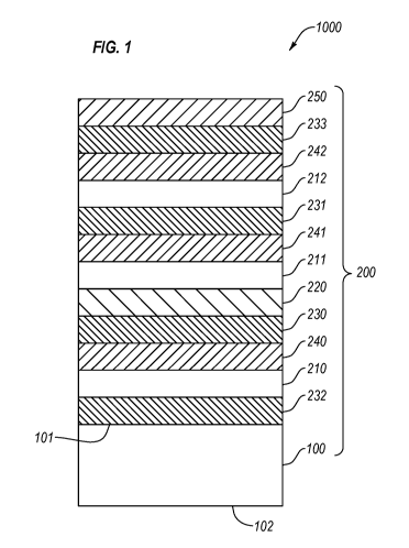
Referring now to FIG. 1, an exemplary embodiment of a coated substrate of the
invention is
shown schematically. Coated substrate 1000 includes a substrate 100 having
first major side 101
and second major side 102. First major side 101 includes a coating 200
disposed thereon.
Coating 200 includes twelve discrete layers. The coating 200 may have a total
thickness of less
than 4000 A, such as between 2000 A and 3000 A. Coating 200 is transparent or
substantially
transparent to visible light. The coating 200 reflects a portion of radiant
infrared energy, thus
tending to keep radiant heat on the same side of the substrate from which it
originated.
12
CA 03019958 2018-10-03
=
WO 2017/184568
PCT/US2017/028071
Coating 200 comprises a plurality of layers. The coating is arranged in a
layer system, or stack,
as schematically shown in FIG. 1. The coating or stack 200 may be deposited on
and/or attached
to the substrate 100. The thickness of one or more layers making up coating
200 may be
continuous, may be uniform, or may vary. The thickness of an individual layer
may vary across
one or more of its width or length. In one example, the film region or a
portion thereof may have
or include a gradual change or graded thickness across at least a portion
thereof. For example,
one or more layers may, in some instances, increase in thickness or decrease
in thickness in one
or more regions of the coated surface. The thickness of an individual layer
may vary between
any of the specific layer thicknesses disclosed herein, such as between any of
the endpoints of
ranges of corresponding layer thicknesses disclosed herein. The one or more
layers may be
provided in a contiguous relationship, that is, arranged directly on top of
and substantially
contacting an adjacent layer or a substrate major surface.
Coating 200 may include three reflective layers 210, 211, 212. First
reflective layer 210 may be
proximal to but not contiguous to the substrate first major surface 101 and
may be the bottom
reflective layer. Third reflective layer 212 may be disposed near the top of
the stack and may be
the topmost of the three reflective layers. Second reflective layer 211 may be
disposed between
first reflective layer 210 and third reflective layer 212. Each of the first,
second, and third
reflective layers may be discrete layers. For example, the three reflective
layers may not
substantially contact one another. In such embodiments, first reflective layer
210 may be about
50 A to 100 A thick, second reflective layer 211 may be about 90 A to 130 A
thick, and third
reflective layer 212 may be about 100 A to 150 A thick. In embodiments, one or
more of the
reflective layers may consist essentially of silver.
Coating 200 may further include an alloy layer 220. Alloy layer 220 may be
disposed between
first and second reflective layers 210, 211 and may be contiguous to second
reflective layer 211.
In such embodiments, alloy layer 220 may be about 10 A to 30 A thick. In
embodiments, alloy
layer 220 may comprise or consist essentially of a nickel alloy such as an NCM
alloy.
Coating 200 may further include at least four oxide layers 230, 231, 232, 233.
First oxide layer
230 may be disposed between first reflective layer 210 and second reflective
layer 211. Second
oxide layer 231 may be disposed between second reflective layer 211 and third
reflective layer
212. Third oxide layer 232 may be disposed contiguous to the substrate first
major surface 101
13
CA 03019958 2018-10-03
=
WO 2017/184568
PCT/US2017/028071
and beneath first reflective layer 210. Fourth oxide layer 233 may be disposed
over the third
reflective layer 212. In such embodiments, first oxide layer 230 may be about
750 A to 850 A
thick, second oxide layer 231 may be about 550 A to 650 A thick, third oxide
layer 232 may be
about 150 A to 300 A thick, and fourth oxide layer 233 may be about 125 A to
175 A thick. In
embodiments, one or more of the oxide layers may comprise or consist
essentially of tin oxide
(Sn02). In embodiments, one or more of the oxide layers may comprise or
consist essentially of
zinc oxide (Zn0). In embodiments, one or more of the oxide layers may comprise
a mixture of
SnO2 and ZnO.
Coating 200 may further includes at least three barrier layers 240, 241, 242.
First barrier layer
240 may be disposed on top of and contiguous to first reflective layer 210.
Second barrier layer
241 may be disposed on top of and contiguous to second reflective layer 211.
Third barrier layer
242 may be disposed on top of and contiguous to third reflective layer 212. In
such
embodiments, first, second, and third barrier layers 240, 241, 242 may each be
about 10 A to 30
A thick. In embodiments, one or more of first, second, and third barrier
layers 240, 241, 242
may comprise or consist essentially of titanium.
Coating 200 may further include functional top layer 250. Functional top layer
250 may be
disposed on top of fourth oxide layer 233 and may be the top layer of the
stack of layers making
up coating 200 (e.g., distal most layer from the substrate). In such
embodiments, top layer 250
may be about 120 A to 150 A thick. In embodiments, the top layer 250 may
comprise or consist
essentially of TiOx or Si3N4.
The coating 200, and other coatings disclosed herein are suitably applied to
any transparent,
substantially transparent, or light transmissive substrate such as substrate
100. The substrate is
suitable for use in a variety of arrangements and settings where control of
reflectance and
transmittance of electromagnetic radiation is required or desired. Thus, in
some embodiments, a
coated substrate as disclosed herein may be a window, a protective covering
(such as for a digital
or other luminous or backlit display) or a skylight. In embodiments, the
coated substrates are
useful and are selectively arranged in terms of one or more of coating
composition, layer
composition, layer placement, layer thickness, and the like to obtain optimal
control of
reflectance and transmittance of electromagnetic radiation.
14
CA 03019958 2018-10-03
=
WO 2017/184568
PCT/1JS2017/028071
In embodiments, a coated substrate of the invention may be employed as a
window pane. In
such embodiments, the coated substrate may be arranged within an insulating
glass ("IG") unit.
IG units include at least two window panes situated substantially parallel to
each other, with
supporting infrastructure to provide a substantially enclosed or sealed space
between the window
panes. Such enclosed or sealed space is often substantially filled with no air
(vacuum), air, an
inert gas such as Argon, or a mixture of air and one or more inert gases. In
such embodiments,
one or both of the window panes of an IG unit may comprise any of the coatings
disclosed herein
on one or both major surfaces thereof In some embodiments, any of the coatings
disclosed
herein may be applied on the first major surface of a first glass substrate,
and the first major
surface of first glass substrate may be arranged to contact the enclosed or
sealed space between
the window panes of an IG unit. The IG unit may further include at least a
second glass substrate
that does not include a coating of the invention. Other suitable arrangements
are easily
envisioned by those of skill. For example, the first and second window panes
in IG units may
suitably include one or more coatings of the invention as described herein,
and/or one or more
additional coatings applied for some other purpose such as antireflectivity,
N1R reflectivity,
privacy, scratch resistance, and the like.
In embodiments, an IG unit may include at least two substrates, such as any of
the substrates
disclose herein. Each of the substrates may include one or more major
surfaces, which may be
substantially parallel to each other. In embodiments, the IG unit may include
a substrate
mounting unit (e.g., window frame, window sash, spacers, seals, etc.),
containing the at least two
substrates therein. The substrate mounting unit may hold the two substrates in
a substantially
parallel configuration. The substrate mounting unit and at least two
substrates may collectively
form an enclosed space therebetween.
FIG. 2 is a schematic diagram showing an IG unit configuration according to an
embodiment.
IG unit 10000 includes first exterior surface 10001 and second exterior
surface 10002, coated
substrate 1000, and additional substrate 2000, wherein surfaces 10001 and
10002 may be
situated substantially parallel to each other. Substrates 1000, 2000 may
partially define enclosed
space 3000. Additional infrastructure to define the enclosed space 3000 is
arranged around IG
unit 10000 in conventional fashion such as in a substrate mounting unit.
Enclosed space 3000
may comprise substantially no air (vacuum), air, an inert gas, or a mixture of
air and one or more
inert gases. Coated substrate 1000 may include coating 200 on substrate 100
first surface 101,
CA 03019958 2018-10-03
WO 2017/184568
PC1/US2017/028071
=
such that coating 200 contacts enclosed space 3000. In embodiments, light
traveling from the
surface 10001 to the surface 10002 (e.g., from outside a building to inside a
building) may
encounter a base layer (e.g., lowermost layer adjacent to the substrate) of
the coating 200 first.
In embodiments, the coating may be disposed on the additional substrate 2000
such that light
traveling from the surface 10001 to the surface 10002 may encounter a top
layer (e.g., uppermost
layer) of the coating 200 first.
The coatings disclosed herein may be disposed on a substrate using any
suitable thin film
deposition methods known to those of skill. In embodiments, a sputtering
technique may be
employed to deposit, dispose, or apply one or more layers of a coating stack.
In such
embodiments, sputtering may be employed to deposit, dispose, or apply each of
the 6 to 20
layers of the coating stack. Sputtering is a technique used to deposit thin
films of a material onto
a surface or substrate. By first creating a gaseous plasma and then
accelerating the ions from this
plasma into a source material, the source material is eroded by the arriving
ions via energy
transfer and is ejected in the form of neutral particles as either individual
atoms or clusters of
atoms or molecules. As these neutral particles are ejected they travel in a
straight line unless
they come into contact with something, whether it is another particle or a
nearby surface. A
substrate as described herein, placed in the path of these ejected particles
will be coated by a
layer thereof. Gaseous plasma is a dynamic condition where neutral gas atoms,
ions, electrons
and photons exist in near balanced state simultaneously. One can create this
dynamic condition
by metering a gas, such as argon or oxygen into a pre-pumped vacuum chamber
and allowing the
chamber pressure to reach a specific level and then introducing a live
electrode into this low
pressure gas environment using a vacuum feed through. An energy source, such
as RF, AC, or
DC may be used to feed and thus maintain the plasma state as the plasma loses
energy into its
surroundings. In embodiments, the type of sputtering used may be diode
sputtering, magnetron
sputtering, confocal sputtering, direct sputtering or other suitable
techniques.
In embodiments, sputtering may be carried out in a batchwise, semi-continuous,
or continuous
process. Semi-continuous and continuous processes involve conveying the light-
transmissive
substrate through a series of two or more zones or chambers wherein layers are
applied
sequentially during the conveying. Where the substrate is e.g. a plate or
sheet of glass, such
processes are semi-continuous; where the substrate is e.g. a roll of polyester
film such processes
are continuous. In both semi-continuous and continuous processes, the rate of
conveyance of a
16
CA 03019958 2018-10-03
=
WO 2017/184568
PCT/US2017/028071
substrate through the apparatus can be adjusted by the operator to vary layer
or coating thickness,
which provides an additional variable for production in addition to varying
the power applied to
the targets during the sputtering. In batchwise processes, the operator can
adjust layer thickness
by varying power applied to targets or dwell time in a zone or chamber.
Reflective layers, alloy layers, and barrier layers may be suitably sputtered
from the
corresponding metallic sources within a substantially inert atmosphere. Oxide
layers and in
some embodiments functional top layers may be suitably sputtered from a
corresponding
dielectric source or by sputtering a metal target in a reactive atmosphere.
For example, to
deposit zinc oxide, a zinc target can be sputtered in an oxidizing atmosphere,
or to deposit a
silicon nitride layer, a silicon target can be sputtered in a nitrogen
atmosphere. Thus in
embodiments, one or more oxide or nitride layers of one or more coating layer
stacks may be
applied by sputtering from the corresponding oxide source or by sputtering a
metal target in a
reactive atmosphere. Top layers suitably include metal, metal oxide, or metal
nitride and the
corresponding source is employed consistent with the intended layer
composition.
In embodiments, chemical vapor deposition (CVD) may be used to dispose one or
more layers of
a coating on a substrate. CVD involves the decomposition of gaseous sources
via a plasma and
subsequent layer deposition onto the substrate. Deposition zones may be
suitably arranged
similarly to a magnetron sputtering system, such that the layer thickness
disposed on the
substrate may be adjusted by varying the speed of the substrate as it passes
through the one or
more plasma zones, and/or by varying the power and/or gas flow rate within
each of the one or
more plasma zones.
The coated substrates disclosed herein provide advantages over currently
available NW
reflective substrates, particularly substrates coated with conventional triple
silver coatings. The
coatings disclosed herein offers the advantages associated with triple silver
coatings such as
favorable solar heat gain / visible light ratios. The coated substrates
disclosed herein have the
color, transparency, and other visible advantages associated with the use of
alloy and superalloy
coatings in conjunction with triple silver coatings, while exhibiting reduced
blue/green color
shift at one or more acute angles from the normal viewing surface of a light
transmissive coated
substrate compared to conventional triple silver coatings. The coated
substrates disclosed herein
17
CA 03019958 2018-10-03
=
WO 2017/184568
PCT/US2017/028071
are readily manufactured using techniques that allow for ease of control of
layer thicknesses
which in turn allows control over acute angle viewing properties.
The coatings disclosed herein reduce color inconsistency when viewed normal to
the glass
surface vs. at acute angles. The color coordinate values of the coated article
from a direction that
is substantially normal to a coated major substrate surface (defined as 00)
may be substantially
equal to the color coordinate values from directions that are acute to the
coated major surface,
such as at angles of about 100 to 89 , or about 15 to 89 , or about 20 to 89
, or about 25 to
89 , or about 30 to 89 , or about 350 to 89 , or about 40 to 89 , or about
45 to 89 , or about
50 to 89 , or about 55 to 89 , or about 60 to 89 , or about 65 to 89 , or
about 70 to 89 , or
about 75 to 89 , or about 80 to 89 , or about 85 to 89 , or about 10 to 85
, or about 10 to
80 , or about 10 to 75 , or about 10 to 70 , or about 10 to 65 , or about
10 to 60 , or about
150 to 85 , or about 150 to 80 , or about 150 to 75 , or any subrange thereof.
In embodiments,
the variation in color coordinate values of the article from a direction that
is substantially normal
to the coated major surface to the color coordinate values from directions
that are acute to the
coated major surface may be reduced relative to known coated articles. To this
end, the coatings
disclosed herein appeal to a wide range of designs and building applications.
The coated substrates disclosed herein are transmissive to visible light, and
may be opaque or
substantially opaque to infrared radiation. The coatings disclosed herein may
provide a visible
light transmission in the range of about 20% to about 60%. Furthermore, the
coatings may
provide a Light to Solar Gain Ratio (LSG) (visible Light Transmittance divided
by the Solar
Heat Gain Coefficient) of approximately 1.7 to 2.3, or about 1.8 to 2.3, or
about 1.9 to 2.3, or
about 2.0 to 2.3, or about 2.1 to 2.3, or about 1.9 to 2.2, or about 1.9 to
2.1, or about 1.9 to 2Ø
An IG unit including a coated substrate of the invention has an improved solar
heat gain
coefficient (SHGC) relative to both the conventional double and triple silver
coated IG units,
while maintaining a desirable visual light transmittance (-50% or greater),
and further includes
improved acute angle viewing properties as described above.
Working Example
A glass sheet (0.25" thick clear standard window glass) was coated by applying
twelve discrete
layers by magnetron sputtering. The layers were applied in the order and at
the layer thickness
18
CA 03019958 2018-10-03
=
WO 2017/184568 PCT/1JS2017/028071
shown in Table 1. Layer 1 was deposited directly on the glass sheet with
each of the subsequent
layers disposed thereon in the order listed.
Table 1. Layers applied and thickness of each layer.
Layer No. Layer composition Layer thickness, A
1 ZnO and SnO2 220
2 Ag 75
3 Ti 20
4 ZnO and SnO2 780
5 INCONEL 625 15
6 AG 110
7 Ti 20
8 ZnO and SnO2 580
9 Ag 130
Ti 20
11 ZnO and SnO2 140
12 TiOx 140
Two glass samples were coated in this manner. Additional triple-silver coated
glass substrates
10 were obtained from commercial sources in the open market (each having a
different
configuration than the coating of Table 1); these were assigned identification
as Samples 2 and 4
as indicated in Table 2.
Each coated glass sheet was mounted in an IG unit, wherein each of the IG
units was configured
in the same way as the IG unit of FIG. 2. Specifically, the coated side of the
coated glass sheets
were situated with the coating contacting the substrate 1000 and the enclosed
space defined by
the IG unit. Thus each IG unit 10000 includes first exterior surface 10001;
second exterior
surface 10002; coated substrate 1000 which is e.g. the coated substrate of
Table 1, a modified
version thereof, or a commercially available triple-silver coated substrate;
and an additional
substrate 2000, wherein substrate surfaces 10001 and 10002 are situated
substantially parallel to
each other. Substrates 1000, 2000 partially define enclosed space 3000;
additional infrastructure
19
CA 03019958 2018-10-03
=
WO 2017/184568
PCT/US2017/028071
to define the enclosed space 3000 is arranged around IG unit 10000 in
conventional fashion.
Each coated substrate 1000 includes a coating on substrate 100 first surface
101, such that the
coating contacts enclosed space 3000. The IG units were arranged such that the
substrate 1000 is
outermost in relation to an outer surface of the building (e.g., contacts the
exterior environment
of the building) in which the IG unit is mounted, making the substrate 2000
interior to the first
substrate 1000 and building the IG unit is mounted on.
Table 2. Coated glass mounted in IG units for testing
IG Sample Coating
1 Coating of Table 1
2 Commercially available triple silver coated
soda glass (first source)
3 Coating of Table 1, but without INCONEL
4 Commercially available triple silver coated
soda glass (second source)
5 Coating of Table 1
Each of the five IG samples (e.g., window units) were mounted side-by-side in
a south-facing
building window for testing purposes. The testing setup for a single IG
sample, e.g. Sample 1, is
.. shown in FIG. 3. Single-story building 10 is shown from the top. IG unit
10000 was mounted in
opening 20 of building 10. The IG unit 10000 was configured the -same as the
IG unit of FIG. 2.
The orientation of the IG unit 10000 in building 10 was such that additional
substrate 2000
contacts the interior environment inside building 10.
Testing of the IG samples were conducted as follows. From a point 21 on the
exterior of
building 10 where the IG samples to be tested are mounted, distance 40 was
measured from the
exterior surface of building 10 at angles 50, 51, 52, and 53. Distance 40 is
12.2 meters (40 feet);
angle 50 is 00 (normal); angle 51 is 30 from normal; angle 52 is 60 from
normal; and angle 53
is 75 from normal. Thus position 60 is situated 12.2 meters from window
opening 20 of
building 10 and at angle 50 (0 ) thereto. Position 61 is situated 12.2 meters
from window
opening 20 of building 10 and at angle 51 thereto. Position 62 is situated
12.2 meters from
CA 03019958 2018-10-03
W02017/184568 PCT/US2017/028071
=
window opening 20 of building 10 and at angle 52 thereto. And position 63 is
situated 12.2
meters from window opening 20 of building 10 and at angle 53 thereto.
Individuals participating in the test were unaware of the identity of any of
IG samples 1-5. Each
individual was instructed to stand at each position 60, 61, 62, 63 and observe
the apparent color
of Samples 1-5; each Sample at each position was then assigned a rating 1-5
based on apparent
observed color shift: 1 - little or no color shift; 2 - slight color shift; 3 -
moderate color shift; 4-
significant color shift; 5 - maximum color shift. Color shift was evaluated
relative to normal for
each sample; that is, position 60 is the baseline against which comparison at
each position 61, 62,
63 is made, wherein each comparison is made with a single sample evaluated at
different angles.
Results of seven individual evaluations are shown in Table 3 and depicted
graphically in FIG. 4.
FIG. 5 includes photos of the IG samples 1-5 at each of positions 60, 61, 62,
63 are shown in
FIG. 5.
21
CA 03019958 2018-10-03
. .
WO 2017/184568 ' PCT/US2017/028071
Table 3. Evaluations of IG samples for color shift as a function of position.
..
Rank, by Individual Evaluator
Sam . le Position CB AT PA AU KS ES SS
Avera: e
60
1.00
1 61 2 1 1 1 1 3
1 , 1.43
62 4 , 1 4 2 1 2 1 2.14
_
63 5 1 5 2 1 1 1 2.29
60 1.00
2 61 1 1 1 2 4 1 1
1.57
62 1 3 1 3 3 1 2 2.00
63 4 4 3 4 2 3 3 3.29
60 1.00
61 1 1 1 1 , 2 1 1 1.14
3 _
62 2 2 1 2 2 1 1 1.57
63 5 3 1 3 3 1 2 2.57
60 1.00
61 1 1 . 1 1 3 ., 2 3 1.71
4
_
62 2 4 1 3 5 2 4 , 3.00 ,
63 5 4 2 3 5 1 3 3.29
60 1.00
61 1 1 1 1 1 2 2 1.29 ,
5 _
62 1 1 1 1 1 _ 1 , 3 1.29
63 2 1 1 2 1 1 3 1.57
As shown in table 3, 1G samples 1 and 5, having the coating of table 1, showed
the
lowest average scores for perceived deviation of color at acute angles. IG
sample 5
showed particularly low deviation scores. The commercially available coatings
of IG
samples 2 and 4 showed the highest average scores.
-22-