Note: Descriptions are shown in the official language in which they were submitted.
CA 03021046 2018-10-12
WO 2017/184760 PCT/US2017/028405
1
METHODS, APPARATUSES, AND ELECTRODES FOR
CARBIDE-TO-CARBON CONVERSION WITH
NANOSTRUCTURED CARBIDE CHEMICAL COMPOUNDS
BACKGROUND
Carbon materials and nanomaterials are an increasingly important
area of materials science and technology. Examples of important carbon
nanomaterials include, for example, fullerenes, carbon nanotubes,
graphene, and nanocrystalline diamond. Carbide-to-carbon reactions and
so-called "carbide-derived carbon" (CDC) are known in the art. However,
better methods are needed to prepare and control such carbon materials,
particularly at the nanoscale. Moreover, it is desirable if reaction
conditions
such as temperature and pressure can be mild and economically attractive.
For example, some preparation methods suffer from a need for high or low
temperatures, or high or low pressures, in addition to a lack of control over
the product. Other preparation methods require use of chemical such as
chlorine which raise environmental and health risks.
SUMMARY
Aspects and embodiment described herein include materials,
methods of making materials, methods of using materials, and devices,
apparatuses, and systems which comprise such materials.
A first aspect, for example, is a method comprising: providing at least
one carbide chemical compound and reducing at least one reactant with
CA 03021046 2018-10-12
WO 2017/184760 PCT/US2017/028405
2
use of the carbide chemical compound to form elemental carbon, wherein
the carbide chemical compound is nanostructured.
A second aspect is a method comprising: producing elemental
carbon material from the oxidation of carbide in at least one carbide
chemical compound in at least one anode of an electrochemical cell
apparatus, wherein the carbide chemical compound is nanostructured.
A third aspect is an apparatus comprising at least one
electrochemical cell comprising: at least one anode comprising at least
one carbide chemical compound, and at least one cathode, wherein the
carbide chemical compound is nanostructured.
A fourth aspect provides for an electrode structure comprising at least
one carbide chemical compound, wherein the carbide chemical compound
is nanostructured.
Still further, a fifth aspect provides for a method comprising operating
at least one anode in an electrochemical cell, wherein the anode comprises
at least carbide chemical compound, wherein the carbide chemical
compound is nanostructured.
Still further, a sixth aspect provides for a method comprising:
producing elemental carbon material from the oxidation of carbide in at
least one carbide chemical compound which is in contact with a melt
comprising at least one salt comprising at least one metal cation which is
reduced, wherein the carbide chemical compound is nanostructured.
Still further, a seventh aspect provides for a method comprising:
producing elemental carbon material from the oxidation of carbide in at
least one carbide chemical compound which is in contact with a solution
comprising at least one organic solvent and at least one dissolved salt
CA 03021046 2018-10-12
WO 2017/184760 PCT/US2017/028405
3
comprising at least one metal cation which is reduced, wherein the carbide
chemical compound is nanostructured.
An eighth aspect is an elemental carbon material composition
prepared by any of the methods described or claimed herein.
A ninth aspect is a method comprising: processing at least one
carbide chemical compound into a nanostructured form of the carbide
chemical compound.
A tenth aspect is a composition comprising, consisting essentially of,
or consisting of nanostructured carbide chemical compound such as, for
example, calcium carbide.
Additional embodiments of these various aspects are provided in the
following detailed description and claims.
At least one advantage which results from at least one embodiment
described herein is better control over the reaction and the reaction product
including control at the nanoscale. This can provide for new forms of
carbon for at least some embodiments.
BRIEF DESCRIPTION OF FIGURES
Figure 1 illustrates in cross-section one embodiment for a
nanostructured carbide chemical compound in nanoparticle form (D is
diameter which will be less than 1,000 nm).
Figure 2 illustrates in perspective view one embodiment for a
nanostructured carbide chemical compound in an elongated form, including
a nanowire (D is width which will be less than 1,000 nm).
CA 03021046 2018-10-12
WO 2017/184760 PCT/US2017/028405
4
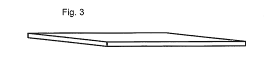
Figure 3 illustrates one embodiment for a nanostructured carbide
chemical compound in a nanofilm form. The film thickness will be less than
1,000 nm.
DETAILED DESCRIPTION
INTRODUCTION
Further details of the various embodiments are provided herein.
References cited herein are incorporated herein by reference in the
entirety. No admission is made that any of the references are prior art.
In addition, the claim transitions "comprising," "consisting essentially
of," and "consisting of" can be used to describe and/or claim the various
embodiments described herein, whether for methods, compositions, or
apparatuses. Basic and novel features of the invention are described .
herein and allow for exclusion of components from claimed embodiments.
Claims can be open, partially closed, or closed claims.
Carbide chemical compounds are known to be used in steel
manufacturing, but an embodiment is that the methods and compositions
described herein do not relate to the manufacture of steel.
CARBIDE-TO-CARBON CONVERSION REACTION
The carbide-to-carbon conversion reaction, and related reactions, are
generally known in the art as reflected in the following references, which
are incorporated herein by reference in the entirety:
US App. No. 14/213,533, filed March 14, 2014 and published as
2014/0271441, describes a method of making carbon from carbide and
CA 03021046 2018-10-12
WO 2017/184760 PCT/US2017/028405
molten, metal salts in a thermal process but at relatively low temperature
compared to prior art processes. PCT Application PCT/US2014/028755,
filed March 14, 2014 and published as WO 2014/144374, also describes a
method of making carbon from carbide and molten, metal salts in a thermal
process but at a relatively low temperature. Also described are processing
steps to purify and treat the elemental carbon material. Figures 6 and 7
show examples of elemental carbon materials prepared by these methods;
US patent application 14/886,319 filed October 19, 2015 described a
method for making carbon from carbide at mild temperature and pressure,
including use of an electrochemical apparatus at room temperature and
pressure, as well as use of a solvent process. Application 14/886,319
describes embodiments for methods of making the carbon, apparatuses for
making the carbon, carbide electrodes, reaction products, post reaction
processing, and applications which are supported by figures, data, and
working examples, all of which is incorporated herein by reference in its
entirety;
Y. Gogotsi, (Ed.), Carbon Nanomaterials, 2006, Chapter 6, "Carbide-
Derived Carbon," (G. Yushin et al.), pp. 211-254;
Carbon Nanomaterials, 2nd Ed., CRC Press, 2014, Chapter 11,
"Carbide-Derived Carbon," (Y. Korenblit et al.), pp. 303-329;
D. Osetzky, Carbon, 12, 517-523, 1974;
N.F. Fedorov, et al., J. App!. Chem. USSR, 54, 2253-2255, 1981;
N.F. Federov, et al., Russ J. App!. Chem. 71, 584-588, 1998;
N.F. Federov, et al., Russ. J. App!. Chem. 71, 795-798, 1998;
(Russian) Ivakhnyuk, Z. Prikladnoi Khimii, 60, 852-856, 1987
("Carbon enriched calcium carbide and possibility of its application");
CA 03021046 2018-10-12
WO 2017/184760 PCT/US2017/028405
6
(Russian) lvakhnyuk, Z. Prikladnoi Khimii, 60, 1413-1415, 1987
("Study of properties of carbon derived from calcium carbide in the
presence of nitrogen");
(Russian) Samonin, Z. Prikladnoi Khimii, 60, 2357-2358, 1987 ("On
mechanism of interaction between calcium carbide and metal chlorides");
SU patent 996324;
SU patent 1175869;
Han et at., J. Phys. Chem., 2011, 115, 8923-8927;
US Patent No. 3,066,099;
Dai et al., Mat. Chem. Phys., 112, 2, 2008, 461-465 (CaC2-CDC,
nanostructured carbon by chlorination of CaC at moderate temperatures);
Carbide-derived carbon (CDC) is described in the patent literature
including, for example, US Patent Publications 2001/0047980;
2006/0165584; 2006/0165988; 2008/0219913; 2009/0036302;
2009/0117094; 2009/0258782; 2009/0301902;
In addition, DE 1667532 Greiner (1971) describes what is said to be
low temperature diamond production from an electrochemical system which
can include use of carbide in the electrolyte with use of temperatures of
600 C to 1000 C. However, no data are provided;
Also, US Patent No. 4,738,759 (1988) describes an electrolysis
process wherein calcium carbide can be subjected to electrolysis to form
graphite sponge at the anode. Temperatures are used such as 700 C to
1,000 C;
A Chen M.S. thesis, August 2002, Univ. N. Texas, describes
electrochemical deposition of films of amorphous carbon and diamond like
carbon (DLC). Electrochemical deposition was carried out using a low
temperature (less than -40 C) solution of acetylene in liquid ammonia;
CA 03021046 2018-10-12
WO 2017/184760 PCT/US2017/028405
7
Kulak, Electrochem. Comm., 5, 2003, 301-305 describes room
temperature electrodeposition of very thin, porous film containing carbon
(50-100 nm thick) from a solution of lithium acetylide. However, the
microscopic images of the film indicate a low quality material (Figure 2) and
much of the film is not carbon apparently;
US 2011/0290655 (Nishikiori; Toyota) describes a method for
electrochemically depositing carbon film on an anode substrate using a
molten salt electrolyte bath comprising a carbide ion and applying a DC
voltage to deposit the carbon film. The bath temperature is 250 C to
800 C. The carbon film is said to be mainly amorphous carbon including
graphite-like carbon according to x-ray diffraction.
CARBIDE CHEMICAL COMPOUND
Carbide chemical compounds or "carbides" are generally known in
the art. See, for example, Cotton & Wilkinson, Advanced Inorganic
Chemistry, 4th Ed., 1980, pages 361-363; and Kosolapova, Carbides,
Properties, Production, and Applications, Plenum Press, 1971. This text
classifies types of carbides as saltlike carbides, interstitial carbides, and
covalent carbides. Carbides can also include other elements such as
oxygen in oxycarbides (see, for example, US Patent Nos. 6,514,897 and
5,599,624).
Known carbide chemical compounds include, for example, aluminum,
arsenic, beryllium, boron, calcium, chromium (in five different Cr:C ratios),
cobalt, hafniuim, iron (in seven different Fe:C ratios), lanthanum,
manganese (in two different Mn:C ratios), magnesium (in two different
Mg:C ratios), molybdenum (in three different Mo:C ratios), nickel (in two
different Ni:C ratios), niobium (in two different Nb:C ratios), plutonium (in
CA 03021046 2018-10-12
WO 2017/184760 PCT/US2017/028405
8
two different Pu:C ratios), phosphorous, scandium, silicon, tantalum (in two
different Ta:C ratios), thorium (in two different Th:C ratios), titanium,
tungsten (in two different W:C ratios), uranium (in two different U:C ratios),
vanadium (in two different V:C ratios), and zirconium carbide. Also, a
carbide can form with two different metals such as cobalt tungsten carbide.
In one embodiment, the carbide chemical compound is a salt-like
carbide or an intermediate transition metal carbide. More particularly, the
carbide chemical compound is a salt-like carbide in one embodiment. In
another embodiment, the carbide chemical compound is a methanide, an
acetylide, or a sesquicarbide.
Methanides react with water to produce methane. Methane is a
carbon atom bonded to four hydrogen atoms in an sp3 hybridization. Two
examples of methanides are aluminum carbide (A14C3) and beryllium
carbide (Be2C). Acetylides are salts of the acetylide anion C2-2 and also
have a triple bond between the two carbon atoms. Triple bonded carbon
has an spl hybridization and two examples of acetylides are sodium
carbide (Na2C2) and calcium carbide (CaC2). Sesquicarbides contain the
polyatonnic anion C3-4 and contains carbon atoms with an spl hybridization.
Two examples of sesquicarbides are magnesium carbide (Mg2C3) and
lithium carbide (Li4C3).
Sesquicarbides are of particular use for the preparation of spl
carbon. One can produce Mg2C3 in the laboratory by bubbling methane
through molten magnesium metal under an inert argon atmosphere at over
750 C. Other hydrocarbons such as pentane may also be viable
candidates. Also, molten magnesium (Mg) reaction is another area of
chemistry where little has been conducted. Research in molten Mg
reactions have been limited because of the dangers associated with molten
CA 03021046 2018-10-12
WO 2017/184760 PCT/US2017/028405
9
Mg, especially with the process generating hydrogen gas as well. But a
process very similar to the synthesis of the magnesium sesquicarbide can
be used to convert methane directly into carbon in the form of graphite and
hydrogen gas. Methane can be bubbled through a molten solution of Mg
and magnesium chloride salt. When heated to a temperature of over 750 C
under an argon atmosphere the elemental Mg metal and MgCl2 both melt
to form a liquid solution. Similar to the Mg sesquacarbide synthesis,
methane is bubbled through the solution to produce either MgC2
(magnesium carbide) or Mg2C3 and hydrogen gas that can be collected as
a value added product. The carbide then reacts with the metallic salt based
on the original chemistry of the carbon producing carbide reaction. The
Mg2C3 and MgCl2 are converted to elemental carbon in the form of
graphite, elemental Mg metal and MgCl2, which would remain as part of the
liquid solution. Therefore, the Mg metal and MgCl2 salt would remain
unchanged throughout the overall process while the methane would be
converted to pure carbon and hydrogen gas.
In particular embodiments, the carbide chemical compound is calcium
carbide, aluminum carbide, sodium carbide, magnesium carbide, lithium
carbide, beryllium carbide, iron carbide, copper carbide, and chromium
carbide. Sodium carbide has the advantage of being lighter.
In other more particular embodiments, the carbide chemical
compound is calcium carbide or aluminum carbide. Calcium carbide is
particularly preferred.
In another embodiment, the carbide chemical compound has
sufficient electronic conductivity to function as or in an anode. The
conductivity for different carbides can vary depending on factors such as
purity and temperature. However, one skilled in the art for a particular
CA 03021046 2018-10-12
WO 2017/184760 PCT/US2017/028405
application can determine whether there is sufficient electronic conductivity
and how to adapt the conductivity for the need. For example, the carbide
chemical compound can have an electronic conductivity of at least 10-8
S/cm, or at least 10-7 S/cm, or at least 10-6 S/cm, or at least 10-5 S/cm, or
at
least 10-4 S/cm, or at least 10-3 S/cm, or at least 10-2 S/cm, or at least 10-
1
S/cm, or at least 100 S/cm. The electronic conductivity of calcium carbide
provides a useful benchmark for sufficient conductivity. No particular upper
limit is present except for the limits provided by nature for a particular
carbide.
The form of the carbide chemical compound can also be varied as
described herein with respect to it being nanostructured.
The carbide chemical compound can be used in compositions and
mixed with other ingredients such as binders or conductivity agents to the
extent the desired reaction can be achieved. in some embodiment, more
than one carbide chemical compound can be used.
One can use an electronically conductive binder to hold the pieces or
particles of carbide together. This can, for example, increase the surface
area of the carbide which is in direct contact with a conductive surface.
Electronically conductive binders also can be selected as a way to produce
composite materials where the conductive properties and other
characteristics of the binder can be used to change the characteristics of
elemental carbon material produced. Examples of electronically conductive
binders include conjugated polymers in doped or undoped form such a
polythiophene or a polyaniline. Polymeric binders can be used.
In one embodiment, the carbide chemical compound can be part of
an ink system involving a solvent vehicle. The solvent can be an organic
solvent or water, and mixtures of solvents can be used. Additives can be
CA 03021046 2018-10-12
WO 2017/184760 PCT/US2017/028405
11
used. Nanoparticles can be suspended in the vehicle and stabilizers can
be used. An ink can be useful for processing and forming films.
In one embodiment, the carbide chemical compound is not a covalent
carbide and in another embodiment is not silicon carbide.
The purity of the carbide chemical compound can be made as high as
possible, including, for example, at least 80 wt.%, or at least 85 wt.%, or at
least 90 wt.%, or at least 95 wt.%, or at least 99 wt.%.
Some carbide chemical compounds are commercially available as
"nanopowders." These include, for example, TiC, SiC, tungsten(IV)C,
Cr3C2, TaC, VC, and ZrC.
The crystallinity of the carbide chemical compound is not particularly
limited, whether of uniform or mixed morphology, whether single crystal,
polycrystalline, nanocrystalline, or amorphous.
In a preferred embodiment, the carbide chemical compound is
calcium carbide. The manufacture of calcium carbide from a carbon source
and a calcium source is well-known, particularly at a large manufacturing
scale. Calcium carbide is produced typically at very high temperatures as a
melt phase and then cooled into larger slabs which are then crushed into
particles and classified by particle size. An electric arc furnace is
typically
used to generate the high temperatures. Calcium carbide is well-known to
be reactive to water to form acetylene, and steps can be taken to keep the
calcium carbide away from moisture and air. Because of its reactivity with
moisture to form acetylene, calcium carbide can present an explosion or
fire hazard if not handled properly.
CA 03021046 2018-10-12
WO 2017/184760 PCT/US2017/028405
12
Other methods are available to make calcium carbide such as in a
microwave reactor (Pillai et al., Ind. Eng. Chem. Res., 2015, 54(44), 1001-
11010, 2015).
The reaction of calcium carbide with acetylene has been reported to
useful to produce carbon nanoparticles (Rodygin et al., Chem. Asian J.,
2016, 11, 7, 965-976).
The methods of carbide production can be adapted to provide for
nanostructured forms of the carbide chemical compound. The carbide
chemical compound can be formed directly in nanostructured form, or after
formation, it can be processed into the nanostructured form.
NANOSTRUCTURED
The carbide chemical compound is nanostructured ("nanostructured
carbide chemical compound"), which is a term generally known in the art.
Nanostructures can take various forms including, for example, one-
dimensional, two-dimensional, and three-dimensional forms as known in
the art. In one embodiment, the carbide chemical compound is
nanostructured in one dimension (e.g., a nanofilm); in another embodiment,
the carbide chemical compound is nanostructured in two dimensions (e.g.,
a nanorod or a nanowire); and in another embodiment, the carbide
chemical compound is nanostructured in three dimensions (e.g. a
nanoparticle). Nanostructured carbide chemical compounds are known in
the art as described in references cited herein (e.g., Silicon Carbide
Nanostructures, Fabrication, Structure, and Properties, (Fan, Chu, Eds.),
2014, describing nanoparticles, nanowires, nanotubes, and nanofilms).
Nanostructured and nanostructure does not mean normal, inherent surface
CA 03021046 2018-10-12
WO 2017/184760 PCT/US2017/028405
13
features on a nanoscale which are present in any solid material surface
including a solid carbide chemical compound. Rather, nanostructured and
nanostructures are engineered into the material through formation of, for
example, nanoparticles, nanowires, or nanofilms.
A wide variety of nanostructures are known in the art. The
nanostructures can be, for example, nanoparticles, nanopowders,
nanoclusters, nanofibers, nanowires, nanotubes, nanofilms, nanolines,
nanohorns, nanowhiskers, nanoonions, nanoplatelets, nanorods,
nanosheets, nanorings, nanobelts, nanodiscs, nanotowers, and nanoshells.
Some of these terms can be considered subsets of other terms. In
preferred embodiments, the nanostructured carbide chemical compound is
in the form of at least one nanoparticle, at least one nanowire, at least one
nanotube, at least one nanofilm, or at least one nanoline.
As used herein, a nanowire can be hollow or non-hollow, and a
hollow nanowire can be also called a nanotube. As used herein, a
nanowire having a shorter aspect ratio (length/width) can be called a
nanorod. An aspect ratio of ten can be used to distinguish the nanorod
form of a nanowire from a nanowire which is not a nanorod, but for
purposes herein nanorods are also nanowires. As used herein, a nanofilm
can be a nanoline if the nanofilm has a length much longer than the width,
such as a length which is two, three, or four, or more times longer than the
width.
The nanostructure can be characterized by a dimension such as 1
nm to 1,000 nm, or 1 nm to 500 nm, or 1 nm to 250 nm, or 1 nm to 100
nm, or 1 nm to 50 nm, or 100 nm to 1,000 nm, or 100 nm to 500 nm, or 100
nm to 250 nm, or 250 nm to 500 nm, or 500 nm to 1,000 nm. The
CA 03021046 2018-10-12
WO 2017/184760 PCT/US2017/028405
14
dimension can represent, for example, a diameter or an average diameter
or width, or a thickness or an average thickness.
There is no particular upper or lower limit on the volume of a
particular nanostructure, but the volume can be, for example, less than 20
cubic micron, or less than 10 cubic micron, or less than one cubic micron,
or less than 0.8 cubic micro, less than 0.6 cubic micron, or less than 0.4
cubic micron, or less than 0.2 cubic micron, or less than 0.5 cubic micron,
or less than 0.001 cubic micron.
Mixtures of nanostructures can be used. For example, nanoparticles
can be mixed with nanowires, nanotubes, or nanorods.
The nanostructures can be porous or non-porous.
In one embodiment, the nanostructured carbide chemical compound
is mixed with at least one other different material. The different material
can be within the nanostructure or it can be in a separate structure such as
a separate particle or wire. In one embodiment, the nanostructured carbide
chemical compound is held in a matrix material. The nanostructures can
be compacted before use.
Nanostructuring of the carbide chemical compound can be carried out
with methods going back to the synthesis of the carbide chemical
compound. For example, if the carbide chemical compound is prepared in
a melt state or a soft state, it can be processed in this melt or soft state.
Molding and pressing operations can be used. Molds can be adapted to be
nanostructured. Steps can be taken to reduce exposure of the carbide
chemical compound to air, oxygen, and moisture as it is formed. In
particular, processes for forming calcium carbide can be adapted to
introduce a nanostructured form. For example, US Patent No. 1,889,951
describes a method for cooling calcium carbide, for example, and this
CA 03021046 2018-10-12
WO 2017/184760 PCT/US2017/028405
method can be adapted. US Patent No. 3,201,052 also describes a
process for crushing and cooling calcium carbide blocks. US Patent No.
4,508,666 also describes a process for cooling and comminuting molten
calcium carbide.
El-Naas et al., Plasma Chemistry and Plasma Processing, 18, 3
(1998) describes a solid-phase synthesis of calcium carbide in a plasma
reactor using fine particle reactants to provide a granular product with finer
particle size. For example, calcium oxide can have a 170 micron particle
size and graphite can have a 130 micron particle size.
Additional patent literature for calcium carbide includes
2011/0123428; 2002/0197200; 2005/0170181; 2014/0311292; and
2005/0171370. Known methods can be adapted to form nanostructures in
the nanostructured carbide chemical compound.
NANOPARTICLE
Nanoparticles are generally known in the art. The nanoparticles can
be characterized both by looking at an individual nanoparticle and also
looking at collections of pluralities of nanoparticles, and use of statistics
to
characterize the collection. The nanoparticles can be characterized by a
diameter which is nanostructured. Mixtures of nanoparticles can be used.
Methods known in the art such as SEM and TEM methods can be used to
measure particle size, shape, and diameter. The particle shape can be
generally spherical, or it can be somewhat elongated and not spherical.
For example, in one embodiment, the nanostructured carbide
chemical compound is in the form of at least one nanoparticle, wherein the
at least one nanoparticle is part of a collection of nanoparticles of the
CA 03021046 2018-10-12
WO 2017/184760 PCT/US2017/028405
16
carbide chemical compound having an average diameter of 1 nm to 1,000
nm.
In another example, the nanostructured carbide chemical compound
is in the form of at least one nanoparticle, wherein the at least one
nanoparticle is part of a collection of nanoparticles of the carbide chemical
compound having an average diameter of 100 nm to 1,000 nm.
In another example, the nanostructured carbide chemical compound
is in the form of at least one nanoparticle, wherein the at least one
nanoparticle is part of a collection of nanoparticles of the carbide chemical
compound having an average diameter of 1 nm to 100 nm.
In another example, the nanostructured carbide chemical compound
is in the form of at least one nanoparticle, wherein the at least one
nanoparticle is part of a collection of nanoparticles of the carbide chemical
compound having an average diameter of 500 nm to 1,000 nm.
In another example, the nanostructured carbide chemical compound
is in the form of at least one nanoparticle, wherein the at least one
nanoparticle is part of a collection of nanoparticles of the carbide chemical
compound having an average diameter of 1 nm to 500 nm.
In another embodiment, the nanostructured carbide chemical
compound is in the form of at least one nanoparticle, wherein the at least
one nanoparticle is part of a collection of microparticles of the carbide
chemical compound and nanoparticles of the carbide chemical compound.
In another embodiment, the nanostructured carbide chemical
compound is in the form of at least one nanoparticle, wherein the at least
one nanoparticle is part of a collection of nanoparticles of the carbide
chemical compound which are bound together with a binder.
CA 03021046 2018-10-12
WO 2017/184760 PCT/US2017/028405
17
In one embodiment, the nanostructured carbide chemical compound
is in the form of at least one nanoparticle, wherein the at least one
nanoparticle is part of a collection of nanoparticles of the carbide chemical
compound which are bound together with an electronically conductive
binder.
In another embodiment, the nanostructured carbide chemical
compound is in the form of at least one nanoparticle, wherein the at least
one nanoparticle is part of a collection of nanoparticles of the carbide
chemical compound which are bound together with a polymeric binder.
In one embodiment, the nanostructured carbide chemical compound
is in the form of agglomerated nanoparticles.
In a particularly preferred embodiment, the nanoparticles are calcium
carbide nanoparticles.
Nanoparticles can be formed by grinding processes which reduce the
particle size to the desired nanodimension. Also, a collection of particles
can be separated or classified so that a nanoparticle portion can be
isolated from larger particles such as microparticles.
One process for grinding particles is the Union process which
includes fine grinding done at micron, sub-micron, and nanoscale levels.
Wet grinding and dry grinding can be carried out. See equipment and
literature available from Union Process, Inc. (Akron, OH).
CN1498976 describes a "desulfurizer based on nanocomposite
calcium carbide and calcium oxide for steel. Briefly, it describes a nano-
class composite calcium carbide (or calcium oxide)-based desulfurizing
agent for steel which contains calcium carbide or calcium oxide
nanoparticles (65-95 wt.%), calcareous high-Al cement clinker, and a series
CA 03021046 2018-10-12
WO 2017/184760 PCT/US2017/028405
18
of powders. The high energy Union Process (Ohio) can be used with an
agitating mill with 2 micron particles crushed to 100 nm-class products.
US Patent No. 7,025,945 describes preparation of calcium carbide
minute powder having particle size of several microns or below made
mechanically.
US Patent No. 2,323,597 describes a multistage, continuous process
for grinding calcium carbide.
Vorozhtsov et al. describes Al4C3 nanoparticles made by hot
compaction (Russian J. of Non-Ferrous Metals, 2012, 53, 5, 420).
Streletskii et al., describe mechanochemical synthesis of aluminum
carbide fine powder.
Fe3C nanoparticles are described in Chemistry of Materials, 2010,
22(18), 5340-5344.
Nanostructured Mo2C nanoparticles are described in, Chen et at,
Energy Environ. Sci. 2013, 6, 943.
Nanostructured TaC is described in, for example, de Oliveira et al.,
Sintering Techniques of Materials, 2015, Chapter 6, p. 107 (InTech).
Nanostructured clusters of carbides are described in US Patent No.
7,025,945 and US Patent Publication 2004/0028948. See also Nishi et al.,
Chem. Phys. Letters, 369, 1-2, 198-203 (2003).
An example of a nanoparticle with diameter D is shown in cross-
section in Figure 1, showing an idealized spherical embodiment.
NANOWIRES/NANOTUBES/NANORODS
Nanowires, nanorods, and nanotubes are generally known in the art.
The diameter of the nanowire or nanotube can be a nanodimension. The
CA 03021046 2018-10-12
WO 2017/184760 PCT/US2017/028405
19
aspect of these structures (length to diameter ratio) may be relatively low
compared to conventional nanowire or nanotube structures, and if less than
ten, the nanowire can also be called a nanorod. Also, the carbide chemical
compound can be mixed with one or more other materials that facilitate
production into a nanowire, or nanotube form, helping to allow for
elongation.
In one embodiment, the nanostructured carbide chemical compound
is in the form of at least one nanowire.
In one embodiment, the nanostructured carbide chemical compound
is in the form of at least one nanowire, wherein the at least one nanowire is
part of a collection of nanowires having an average diameter of 1 nm to
1,000 nm.
.
In one embodiment, the nanostructured carbide chemical compound
is in the form of at least one nanowire, wherein the at least one nanowire is
part of a collection of nanowires having an average diameter of 1 nm to 100
nm.
In one embodiment, the nanowire has an aspect ratio of less than
ten, such as 3 to 10. In another embodiment, the aspect ratio is greater
than ten.
In another embodiment, the nanostructured carbide chemical
compound is in the form of at least one nanotube.
In another embodiment, the nanostructured carbide chemical
compound is in the form of at least one nanotube, wherein the at least one
nanotube is part of a collection of nanotubes having an average diameter of
1 nm to 1,000 nm.
In another embodiment, the nanostructured carbide chemical
compound is in the form of at least one nanotube, wherein the at least one
CA 03021046 2018-10-12
WO 2017/184760 PCT/US2017/028405
nanotube is part of a collection of nanotubes having an average diameter of
1 nm to 100 nm.
Particularly preferred embodiments are calcium carbide nanofibers,
calcium carbide nanowires, or calcium carbide nanotubes, or calcium
carbide nanorods.
Nanowires can be prepared by drawing processes.
Chen et al., describe A14C3 nanorods (Adv. Eng. Mat., 2014, 16, 8).
Sun et al., describe A14C3 one-dimensional nanostructures including
nanowires (Nanoscale, 2011, 3, 2978).
Sun et al., describe describe A14C3 one-dimensional nanostructures
including nanowires (ACSNano, 2011, 5, 2, 2011).
He et al, describe fabrication of aluminum carbide nanowires by a
nano-template reaction (Carbon, 48, 2010, 931).
CN101125652 describes a method for synthesizing aluminum carbide
nanobelts.
Zhang et al. describe a self-assembly process for making aluminum
carbide nanowires and nanoribbons.
US Patent No. 6,514,897 describes nanorods having carbides and/or
oxycarbides.
Schmueck et al. describe making nanostructured metal carbides via
salt flux synthesis, including making V807 (Inorganic Chemistry, 2015,
54(8) 3889.
An example of a nanowire is shown in a perspective view in Figure 2,
showing an idealized spherical representation with diameter D.
NANOFILMS AND NANOLINES
CA 03021046 2018-10-12
WO 2017/184760 PCT/US2017/028405
21
Nanofilms and nanolines are generally known in the art. Here, the
thickness dimension can be nanostructured. The line can be linear or
curved as in curvilinear.
In one embodiment, the nanostructured carbide chemical compound
is in the form of at least one nanofilm.
In one embodiment, the nanostructured carbide chemical compound
is in the form of at least one nanofilm, and the nanofilm is in the form of a
nanoline, wherein the line has a line width of 1 mm or less.
In one embodiment, the nanostructured carbide chemical compound
is in the form of at least one nanofilm having an average film thickness of 1
nm to 1,000 nm.
In one embodiment, the nanostructured carbide chemical compound
is in the form of at least one nanofilm having an average film thickness of 1
nm to 100 nm.
In one embodiment, the nanostructured carbide chemical compound
is in the form of at least one nanofilm which is disposed on a substrate.
The substrate can be inorganic or organic material, and can be, for
example, glass, metal, polymeric, ceramic, composite, or other types of
materials. The nanofilms and nanolines can be disposed by deposition on
a solid substrate including a substrate made of inorganic or organic
material. Patterning of the nanofilm or nanoline can be carried out.
In a particularly preferred embodiment, the nanofilms and nanolines
are calcium carbide nanofilms and calcium carbide nanolines.
Nanofilms can be made by pressing molten forms of the carbide
chemical compound. Another method is thin film deposition methods on a
substrate such as sputtering, chemical vapor deposition, ion implantation,
and the like.
CA 03021046 2018-10-12
WO 2017/184760 PCT/US2017/028405
22
Sun et al. describe A14C3 nanowalls (Cryst. Eng. Comm., 2012, 14,
7951).
S. Reynaud describes preparation of boron carbide nanostructured
materials made by sputtering of thin films (PhD thesis, Rutgers Univ.,
2010).
An examples of a nanofilnn is shown in a perspective view in Figure 3.
OXIDATION/REDUCTION REACTION; REACTION CONDITIONS
The oxidation and reduction reactions can be carried out under a
variety of reaction conditions including temperature and pressure. A
reactant is used along with the nanostructured carbide chemical
compound. Many reaction conditions and the apparatuses and reaction
vessels to carry out the reactions are described in patent applications cited
herein including 14/886,319 and PCT Application PCT/US2014/028755.
Several lead embodiments include use of an electrochemical approach,
use of a melt approach, and use of a solvent approach, which are
described more hereinbelow. The electrochemical and solvent approaches
are particularly described in US 14/886,319, and melt approaches are
particularly described in PCT Application PCT/US2014/028755. A reactant
is used which is reduced as the nanostructured carbide chemical
compound is oxidized. The reactant can be, for example, a metal salt in
which the metal cation is reduced from the electrons of the oxidizing
carbide. In some embodiments, the carbide chemical compound can be in
direct, physical contact, wherein for example, the reactant is in a melt or
solution phase and is in direct, physical contact with the carbide chemical
compound. In other embodiments, the reactant and carbide chemical
CA 03021046 2018-10-12
WO 2017/184760 PCT/US2017/028405
23
compound cannot be in direct, physical contact, but indirectly linked via an
electrically conductive pathway in an electrochemical cell.
Relatively low temperatures, including room temperature, can be
used for the reaction to form carbon. For example, the temperature can be,
for example, about -50 C to about 100 C, or about 10 C to about 90 C, or
about 0 C to about 50 C, or about 15 C to about 50 C. The temperature
can be, for example, about 20 C to about 30 C, or about 23 C, 24 C, or
25 C. In some embodiments, one will want if possible to avoid the expense
of cooling, heating, and temperature control elements. In some
embodiments, one will want to run the reaction as close to ambient as
possible. As known in the art, in a larger manufacturing operation, excess
heat from one point in the operation can be transferred to another point in
the operation which needs heat.
In other embodiments, the reducing is carried out at a temperature of
less than about 400 C, or at a temperature of about 15 C to about 400 C.
In other embodiments, the reducing is carried out at a temperature of less
than about 300 C.
In some embodiments, the methods described herein are undertaken
at room temperature.
Moisture free, air free, oxygen free environments can be used for the
reaction, and inert gases can be used.
The pressure can be about 1 atmosphere (760 torr) or normal
pressure. The pressure can be, for example, about 720 torr to about 800
torr. Alternatively, the pressure can be for example about 0.5 atmosphere
to about 5 atmosphere, or about 0.9 atmosphere to about 1.1 atmosphere.
In some embodiments, one will want if possible to avoid the expense of
using pressures below or above normal atmospheric ambient pressure.
CA 03021046 2018-10-12
WO 2017/184760 PCT/US2017/028405
24
One can use a higher pressure to control the boiling point of the solvent.
However, the equipment must be adapted to sustain high or low pressures.
A preferred embodiment is that temperature and pressure both are
about ambient so than expensive methods to control temperature and
pressure are not needed. Hence, for example, the temperature can be
about 20 C to about 30 C, or about 25 C, and the pressure can be about
720 torr to about 800 torr, or about 760 torr.
Other method parameters for the reduction reaction can be varied.
For example, in one embodiment, one or more materials used in the
process can be recycled. The material can be purified as part of the
recycling. For example, solvent can be distilled and recaptured for further
use. Salts can be recaptured and reused.
In another embodiment, the current flow from a process reactor to
make carbon which is run as a galvanic cell can be used to help power
another process reactor, including one used to make elemental carbon
material, in which current is needed to help control the voltage.
The percent yield of the reaction for elemental carbon material
product can be controlled by the amount of current flow and the methods of
isolation as known in the art. Percent yield can be measured with respect
to the amount of carbon in the carbide chemical compound put in the
reactor. In some cases, the yield is at least one percent, or at least 5%, or
at least 10%, or at least 20%.
REACTANT; METAL SALT
The reactant can be, for example, a moiety which can be reduced
such as at least one metal salt, and metal salts are well-known in the art,
CA 03021046 2018-10-12
WO 2017/184760 PCT/US2017/028405
comprising a metal cation and an anion. Organic reactants can also be
used, in principle, if the redox potentials allow for reaction. The reactant
is
selected to react well with the nanostructured carbide chemical compound
to achieve the intended goal for the particular application (e.g., carbon
production).
In one embodiment, the reactant is selected to function in an
electrochemical reaction. In another embodiment, the reactant is selected
to function in a melt reaction. In another embodiment, the reactant is
selected to function in a solution reaction.
In the electrochemical approach, the nanostructured carbide chemical
compound is used in the form of an anode and used in conjunction with a
cathode where the reactant is reduced. For example, the cathode can be
used in conjunction with a solution comprising a dissolved salt including a
metal cation and an anion. In principle, any ion/metal combination where
the ion can be reduced to the metal can be used for a cathode employing
this method. More specifically, in principle, any elemental metal immersed
in a solution containing ions of that metal, where the ions can be reduced to
the elemental state in order to facilitate the oxidation of the carbide ions
to
elemental carbon, can be used. Examples include zinc metal in a solution
of zinc ions, tin metal in a solution of stannous ions, silver metal in a
solution of silver ions, and iron in a solution of ferrous ions. In selecting
the
cathode, practical considerations can be taken into account. For example,
issues like corrosion of the metal cathode can be considered. Other factors
to consider include, for example, the characteristics of the solvent and the
overall solution and how they would interact with the different components
of the reaction system. Solubility of the various metallic salts in the
different solvents or solvent combinations would also be an issue.
CA 03021046 2018-10-12
WO 2017/184760 PCT/US2017/028405
26
In one embodiment, the electrochemical cell (e.g., galvanic cell)
apparatus further comprises at least one metal cathode, wherein the
cathode is a zinc, tin, iron (include steel), copper, or silver metal cathode.
In another embodiment, the electrochemical cell (e.g., galvanic cell)
apparatus further comprises at least one metal cathode, wherein the
cathode is a zinc or tin metal cathode.
In one embodiment, the galvanic cell apparatus anode is contacted
with at least one first solution comprising at least one first solvent and at
least one first salt and a galvanic cell apparatus cathode is also contacted
with at least one second solution comprising at least one second solvent
and at least one second salt. The solvent and salt combination for both the
anode and cathode sides of the cell should provide sufficient ionic
conductivity for the process to be enabled. The viscosity of the solvent can
be also considered in solvent selection for first and second solvent. For
first and second solvent, the solvent can be, for example, a polar organic
solvent such as an alcohol such as methanol or ethanol, or an ether such
as tetrahydrofuran, or an aprotic solvent such as DMSO or NMP.
Examples of solvents include N-methyl pyrrolidone, dimethyl formamide,
acetone, tetrahydrofuran, pyridine, acetonitrile, methanol, ethanol,
tetramethylurea, and/or dichlorobenzene. Mixtures of solvents can be
used. In general, water is avoided in the solvent, and solvents can be
dried. In some cases, slow reaction between the solvent and the carbide
chemical compound may occur. For example, methanol can reaction with
calcium carbide to form calcium methoxide. Typically, the reaction
apparatus should be relatively inert to the solvent so that side reactions are
minimized or avoided.
CA 03021046 2018-10-12
WO 2017/184760 PCT/US2017/028405
27
The salts for the cathode and anode sides of the cell can be selected
to provide the cation or the anion which enable the reaction to work well.
For example, the cathode metal being reduced can be used in conjunction
with a salt which has the oxidized metal as cation. The anion of the salt
can be a halide such as fluoride, chloride, bromide, or iodide. However, the
fluoride can cause a high heat of reaction which can generate problems so
fluoride salts can be avoided. Chloride salts generally are preferred.
Examples of salts include zinc chloride, calcium chloride, stannous
chloride, ferrous chloride, cupric chloride, silver chloride, aluminum
chloride, lithium chloride, calcium fluoride, stannous fluoride, aluminum
fluoride, and lithium fluoride.
An important factor also is that the cation of the carbide must form a
soluble salt with the anion of the cathode cell. This may not be possible in
some cases such as some sulfate salts including calcium sulfate.
ELECTROCHEMICAL CELL METHOD
The electrochemical embodiments are described further. The
method of making can be based on a electrochemical cell apparatus which
can be galvanic (spontaneous reaction) or electrolytic (non-spontaneous
reaction). Preferably, the method makes use of a galvanic reaction using a
galvanic cell apparatus. Preferably, the reaction is a spontaneous redox
reaction. A galvanic reaction is generally known in the art as a
spontaneous redox reaction wherein one moiety is oxidized and another
moiety is reduced. The moieties are connected electrically to allow current
to flow and the redox reaction to occur. A multimeter can be used to
measure voltage and current flow for such a reaction. No external
CA 03021046 2018-10-12
WO 2017/184760 PCT/US2017/028405
28
electrical potential is needed to induce the spontaneous reaction in a
galvanic reaction. However, an external electrical potential can be used to
control or modify the galvanic reaction, while the reaction is still called a
"galvanic reaction" or a "spontaneous reaction." The discharge of the
current flow can be regulated. The galvanic reaction can be a source of
power, voltage, and current, and these reactions can be used to power
other systems and loads as known in the art.
The elements of a method using a galvanic reaction are known and
described more hereinbelow. They include, for example, at least one
anode, at least one cathode, and connections between the anode and
cathode to allow current flow and form a circuit. The connections can
provide electronic or ionic current flow. For example, wiring can be used
and devices can be used to measure the potential and current flow. Ionic
flow can be enabled with use of salt bridges or ion exchange membranes.
The salt bridge or ion exchange membrane can have a geometry and
length which help to determine the rate of the redox reaction. The transport
of the appropriately charged moiety, an anion, can be mediated through the
salt bridge or the ion exchange membrane to complete the circuit. For
instance, in one embodiment, a cation such as a zinc cation dissolved in
the solution in the metal cell cannot migrate or transfer through the ion
exchange membrane. However the anion (e.g., Cl") is able to diffuse
through the membrane and into the carbide cell. In one embodiment, the
salt bridge is replaced with, or used with, or comprises an ion exchange
membrane. In any event, the salt bridge or ion exchange membrane can
be adapted to avoid being a rate limiting step ("bottle neck") for the process
and pass as much charge as possible.
CA 03021046 2018-10-12
WO 2017/184760 PCT/US2017/028405
29
The elements of a method using an electrolytic reaction are also
known.
In one embodiment, the electrochemical cell (e.g., galvanic cell)
apparatus further comprises at least one cathode which can be a metal
cathode. Mixtures of metals can be used.
The cathode can be used in conjunction with a solution comprising a
dissolved salt including a metal cation and an anion. In principle, any
ion/metal combination where the ion can be reduced to the metal can be
used for a cathode employing this method. More specifically, in principle,
any elemental metal immersed in a solution containing ions of that metal,
where the ions can be reduced to the elemental state in order to facilitate
the oxidation of the carbide ions to elemental carbon, can be used.
Examples include zinc metal in a solution of zinc ions, tin metal in a
solution of stannous ions, silver metal in a solution of silver ions, and iron
in
a solution of ferrous ions. In selecting the cathode, practical considerations
can be taken into account. For example, issues like corrosion of the metal
cathode can be considered. Other factors to consider include, for example,
the characteristics of the solvent and the overall solution and how they
would interact with the different components of the reaction system.
Solubility of the various metallic salts in the different solvents or solvent
combinations would also be an issue.
In one embodiment, the electrochemical cell (e.g., galvanic cell)
apparatus further comprises at least one metal cathode, wherein the
cathode is a zinc, tin, iron (include steel), copper, or silver metal cathode.
In another embodiment, the electrochemical cell (e.g., galvanic cell)
apparatus further comprises at least one metal cathode, wherein the
cathode is a zinc or tin metal cathode.
CA 03021046 2018-10-12
WO 2017/184760 PCT/US2017/028405
In one embodiment, the galvanic cell apparatus anode is contacted
with at least one first solution comprising at least one first solvent and at
least one first salt and a galvanic cell apparatus cathode is also contacted
with at least one second solution comprising at least one second solvent
and at least one second salt. The solvent and salt combination for both the
anode and cathode sides of the cell should provide sufficient ionic
conductivity for the process to be enabled. The viscosity of the solvent can
be also considered in solvent selection for first and second solvent. For
first and second solvent, the solvent can be, for example, a polar organic
solvent such as an alcohol such as methanol or ethanol, or an ether such
as tetrahydrofuran, or an aprotic solvent such as DMSO or NMP.
Examples of solvents include N-methyl pyrrolidone, dimethyl formamide,
acetone, tetrahydrofuran, pyridine, acetonitrile, methanol, ethanol,
tetramethylurea, and/or dichlorobenzene. Mixtures of solvents can be
used. In general, water is avoided in the solvent, and solvents can be
dried. In some cases, slow reaction between the solvent and the carbide
chemical compound may occur. For example, methanol can react with
calcium carbide to form calcium methoxide. Typically, the reaction
apparatus should be relatively inert to the solvent so that side reactions are
minimized or avoided.
The salts for the cathode and anode sides of the cell can be selected
to provide the cation or the anion which enable the reaction to work well.
For example, the cathode metal being reduced can be used in conjunction
with a salt which has the oxidized metal as cation. The anion of the salt
can be a halide such as fluoride, chloride, bromide, or iodide. However, the
fluoride can cause a high heat of reaction which can generate problems so
fluoride salts can be avoided. Chloride salts generally are preferred.
CA 03021046 2018-10-12
WO 2017/184760 PCT/US2017/028405
31
Examples of salts include zinc chloride, calcium chloride, stannous
chloride, ferrous chloride, cupric chloride, silver chloride, aluminum
chloride, lithium chloride, calcium fluoride, stannous fluoride, aluminum
fluoride, and lithium fluoride.
An important factor also is that the cation of the carbide must form a
soluble salt with the anion of the cathode cell. This may not be possible in
some cases such as some sulfate salts including calcium sulfate.
In one embodiment, the galvanic cell apparatus further comprises at
least one salt bridge and/or at least one ion exchange membrane. Ion
exchange membranes are known in the art and typically are made of a
polymeric material attached to charged ion groups. Anion exchange
membranes contain fixed cationic groups with mobile anions; they allow the
passage of anions and block cations. Cation exchange membranes contain
fixed anionic groups with mobile cations; they allow the passage of cations
and block anions. See, for example, Y. Tanaka, Ion Exchange
Membranes: Fundamentals and Applications, 2nd Ed., 2015. Herein, the
use of ion exchange membranes can help prevent formation of unwanted
side products and migration of undesired materials from one cell to the
other cell.
In one embodiment, steps are taken so that the reaction is carried out
under anhydrous conditions. Moisture can be excluded to the extent
needed. Also, inert gases can be used such as argon or nitrogen.
The reaction time can be adapted to the need. Reaction time can be,
for example, one minute to 30 days, or one day to 20 days.
In one embodiment, the production of carbon is carried out without
use of an external voltage source. The current flow from the spontaneous
reaction is not controlled by external voltage in this embodiment.
CA 03021046 2018-10-12
WO 2017/184760 PCT/US2017/028405
32
In another embodiment, however, the galvanic cell apparatus
comprises an external voltage source which is used to regulate the
oxidation reaction, and in another embodiment, the production of carbon is
carried out with use of an external voltage source to regulate the oxidation
reaction. This can also be called a "forced current" embodiment. The
application of an external voltage source allows one to control the voltage
over time using a controlled voltage over time curve, including a step curve,
for example. Constant voltage and/or constant current regimes can be
used. Over time, voltage can be increased or decreased. Reaction rate
can be controlled and increased using the external voltage. For example,
reaction rate (current flow in amperage) might increase at least ten times,
or at least twenty times, or at least fifty times, or at least 100 time, or at
least 250 times, for example, with the application of external voltage
compared to cases with no external voltage applied. The level of external
voltage can be determined for a particular system. One wants to avoid side
reactions. One often will want to increase reaction rate. Voltage can be,
for example, 0 V to 40 V, or 0 V to 30 V, or 0 V to 20 V, or 10 V to 20 V.
The external voltage source can be applied with use of a potentiostat as
known in the art.
In one embodiment, the electrochemical cell apparatus is an
electrolytic cell apparatus. Here, the reaction is not spontaneous, and an
external voltage needs to be and is applied to drive the reaction. An
example is making lithium or sodium.
ORGANIC SOLVENT REACTION TO PRODUCE CARBON FROM
CARBIDE
CA 03021046 2018-10-12
WO 2017/184760 PCT/US2017/028405
33
The solution reaction embodiment is described more. Another aspect
is provided for the production of elemental carbon material from
nanostructured carbide chemical compound at normal temperature and
pressure but without an electrochemical apparatus. Here, a method is
provided comprising: producing elemental carbon material from the
oxidation of carbide in at least one nanostructured carbide chemical
compound (e.g., calcium carbide) which is in contact with a solution
comprising at least one organic solvent (e.g., methanol) and at least one
reactant, such as dissolved salt (e.g., calcium chloride), comprising at least
one metal cation which is reduced. If a cation is used, the cation is
selected so that a spontaneous reaction can occur wherein the carbide is
oxidized and the metal cation is reduced. However, in this embodiment,
the molten salt approach and the electrochemical approach described
herein are not used. Rather, in this embodiment, the reaction can be
carried out in a single reaction container and need not be split into two
cells
as is done with the electrochemical reaction.
In this embodiment, the temperature and pressure can be as
described above. Normal temperature and pressure can be used.
However, heat or cooling can be applied if desired.
The carbide chemical compound can be as described herein using,
for example, aluminum carbide or calcium carbide. The selection of salts,
cations, and anions also can be made as described herein.
Examples of the organic solvent include solvents listed herein for the
electrochemical reaction such as an alcohol such as methanol or ethanol
as described herein. Polar solvents are needed which can dissolve a salt.
A protic solvents can be used. Ideally, the solvent would not react with
CA 03021046 2018-10-12
WO 2017/184760 PCT/US2017/028405
34
nanostructured carbide chemical compound. Alternatively, it reacts with
carbide but only very slowly.
The elemental carbon material produced is described herein also.
The reaction time can be adapted to the need.
Anhydrous reaction conditions can be used. For example, a dry box
can be used to avoid side reactions with water or oxygen.
APPARATUS
Devices and apparatuses for the reaction of nanostructured carbide
chemical compound can be adapted for the method, e.g., whether an
electrochemical, melt, or solution method.
Another aspect provides for an apparatus which can be used to carry
out the methods described herein, including an apparatus comprising at
least one electrochemical cell comprising: at least one anode comprising at
least one nanostructured carbide chemical compound, and at least one
cathode. This apparatus can be used to carry out the methods described
and/or claimed herein. Carbide electrode structures which can be used in
the apparatus are described further hereinbelow. Elemental carbon
material reaction products are described further hereinbelow. Other
embodiments include methods of making these apparatuses. A plurality of
apparatuses can be used in a larger system if desired.
The electrochemical apparatus can be a galvanic cell apparatus or an
electrolytic cell apparatus. The galvanic cell is preferred.
In one embodiment, the nanostructured carbide chemical compound
is a salt-like carbide or an intermediate transition metal carbide. In one
embodiment, the nanostructured carbide chemical compound is a salt-like
carbide. In one embodiment, the nanostructured carbide chemical
CA 03021046 2018-10-12
WO 2017/184760
PCT/US2017/028405
compound is a methanide, an acetylide, or a sesquicarbide. In one
embodiment, the nanostructured carbide chemical compound is calcium
carbide, aluminum carbide, sodium carbide, magnesium carbide, lithium
carbide, beryllium carbide, iron carbide, copper carbide, and chromium
carbide. In one embodiment, the nanostructured carbide chemical
compound is calcium carbide or aluminum carbide. In one embodiment,
the nanostructured carbide chemical compound has sufficient electronic
conductivity to function as an anode. In one embodiment, the
nanostructured carbide chemical compound has an electronic conductivity
of at least 10-8 S/cm, or at least 107 S/cm, or at least 10-6 S/cm, or at
least
le S/cm, or at least 104 S/cm, or at least 10-3 S/cm, or at least 10-2 S/cm,
or at least 10-1 S/cm, or at least 100 S/cm. The electronic conductivity of
calcium carbide provides a useful benchmark for sufficient conductivity. No
particular upper limit is present except for the limits provided by nature for
a
particular nanostructured carbide.
In one embodiment, the nanostructured carbide chemical compound
is held in a container.
In one embodiment, the galvanic cell apparatus anode is contacted
with a solution comprising at least one solvent and at least one salt.
In one embodiment, the electrochemical cell apparatus anode is
contacted with a solution comprising at least one organic solvent and at
least one dissolved salt, as described above. In one embodiment, the
electrochemical cell apparatus cathode is contacted with a solution
comprising at least one organic solvent and at least one dissolved salt as
'
described above. In one embodiment, the electrochemical cell apparatus
cathode is a metal cathode as described above. in one embodiment, the
electrochemical cell apparatus cathode is a metal cathode, wherein the
CA 03021046 2018-10-12
WO 2017/184760 PCT/US2017/028405
36
metal is zinc, tin, iron, copper, or silver. In one embodiment, the
electrochemical cell apparatus cathode is a metal cathode, wherein the
metal is zinc or tin.
In one embodiment, the electrochemical cell apparatus comprises an
external voltage source to regulate an oxidation reaction of carbide in the
carbide chemical compound. For example, a potentiostat can be used to
provide such an external voltage which can be varied.
In one embodiment, the apparatus is adapted for carrying out the
methods described and/or claimed herein.
THE CARBIDE ELECTRODE STRUCTURE AND METHODS OF USE
The nanostructured carbide chemical compound can be used in and
adapted for use in an electrode structure. Hence, yet another aspect
provides for an electrode structure comprising at least one nanostructured
carbide chemical compound. Optionally the carbide chemical compound is
a salt-like carbide. Optionally, at least one electronically conductive
element different from the carbide chemical compound forms part of the
electrode structure. This electrode structure can be used to carry out the
methods and to prepare the apparatuses described and/or claimed herein.
Embodiments described herein also include methods of making and
methods of using the nanostructured carbide electrode structure. Multiple
electrode structures can be used as part of a larger electrode system. The
shape of the electrode can be varied for the need. The conductivity of the
electrode can be adapted to the need. The solid properties and macro-,
micro-, and nano-scale morphology, such as the size and shapes of
openings, porosity, and pore size, can be adapted to the need.
CA 03021046 2018-10-12
WO 2017/184760 PCT/US2017/028405
37
The solid electrode structure and the nanostructured carbide
chemical compound can be contacted with at least one liquid for a redox
reaction. The electrode structure provides a reaction of the carbide
chemical compound which is not just a surface reaction but can extend to
the internal structure of the carbide chemical compound. While the present
inventions are not limited by theory, it is believed that the carbon carbide
layer of the carbon compound at the surface is reacted to form elemental
carbon material as the cation (e.g, calcium) is transported away from the
carbon into solution. Multiple layers of carbon can be built up. The surface
of the carbide can have some porosity.
The carbide electrode can be an electrode (an anode) where the
chemical reaction can occur within the electrode instead of just at the
surface. The electrode material itself (e.g., calcium carbide) is being
consumed in the reaction where the calcium ion dissolves into the solution
and the elemental carbon material is remaining.
In one embodiment, the carbide chemical compound of the electrode
is a salt-like carbide or an intermediate transition metal carbide. In one
embodiment, the carbide chemical compound is a salt-like carbide. In one
embodiment, the carbide chemical compound is a methanide, an acetylide,
or a sesquicarbide.
In one embodiment, the carbide chemical compound is calcium
carbide, aluminum carbide, sodium carbide, magnesium carbide, lithium
carbide, beryllium carbide, iron carbide, copper carbide, chromium carbide,
and chromium carbide. In one embodiment, the carbide chemical
compound is calcium carbide, aluminum carbide, sodium carbide,
magnesium carbide, lithium carbide, or beryllium carbide. In one
embodiment, the carbide chemical compound is calcium carbide or
CA 03021046 2018-10-12
WO 2017/184760 PCT/US2017/028405
38
aluminum carbide, preferably calcium carbide. In one embodiment, the
carbide chemical compound has sufficient electronic conductivity to
function as an anode. In one embodiment, the carbide chemical compound
has an electronic conductivity of at least 10-8 S/cm or other ranges
described herein such as at least 10-7 S/cm, or at least 10-8 S/cm, or at
least 10-8 S/cm, or at least I 0 S/cm, or at least 10-3 S/cm, or at least 10-2
S/cm, or at least 10-1 S/cm, or at least 100 S/cm. No particular upper limit
is
present except for the limits provided by nature for a particular carbide. In
one embodiment, the carbide chemical compound is an ionically bonded
solid.
In one embodiment, the carbide chemical compound is in the form of
individual pieces or particles which have to be contained within an
electrode structure. In one embodiment, the carbide chemical compound is
produced in a form to provide maximum or large amounts of surface area.
This can facilitate reaction of the carbide at its surface. The particle size
and surface area can be adapted to the multiple needs.
In some embodiments, the carbide chemical compound can be used
with one or more additional, different materials such as an additive.
Materials and additives which are useful for making electrodes can be
used. For example, a binder can be used.
In one embodiment, the nanostructured carbide chemical compound
is held in a container. In one embodiment, the container has openings
which allow fluid, such as an electrolyte, to enter the container and contact
the carbide chemical compound. Of course, the container must be able to
contain the nanostructured carbide chemical compound.
CA 03021046 2018-10-12
WO 2017/184760 PCT/US2017/028405
39
In one embodiment, the nanostructured carbide chemical compound
is divided into portions. In one embodiment, the carbide chemical
compound is divided into approximately equal portions.
In one embodiment, the nanostructured carbide chemical compound
used in the electrode is at least about 80 wt.% pure, or at least 90 wt. %
pure, or at least 95 wt. % pure, or at least 97 wt. % pure.
The electronically conductive element should have good electronic
conductivity such as, for example, at least 10-3 S/cm, or at least 10-2 S/cm,
or at least 10-1S/cm, or at least 100 S/cm.
In one embodiment, the electronically conductive element is a binder
for the carbide chemical compound.
In one embodiment, the electronically conductive element is adapted
to be non-reactive with the reaction media. For example, it should be inert
to the contacting solution, or at least inert enough to effectively conduct
the
reaction for the need.
In one embodiment, the electronically conductive element is a
container and the carbide chemical compound is held in the container.
In one embodiment, the electronically conductive element is a
metallic container and the carbide chemical compound is held in the
metallic container. In one embodiment, the electronically conductive
element is a non-metallic container such as graphite and the carbide
chemical compound is held in the non-metallic container such as graphite.
For example, graphite baskets can be used.
In one embodiment, the electronically conductive element comprises
at least one conductive rod.
In one embodiment, the electrode structure is adapted to be
removably attached to an apparatus.
CA 03021046 2018-10-12
WO 2017/184760 PCT/US2017/028405
In one embodiment, the electronically conductive element of the
electrode structure comprises at least one current collector.
In one embodiment, the electrode structure is adapted for use as an
anode in, for example, an electrochemical cell apparatus.
For example, provided is a method comprising operating at least one
anode in an electrochemical cell, wherein the anode comprises at least
carbide chemical compound which includes a method comprising operating
at least one anode in a galvanic cell, wherein the anode comprises at least
carbide chemical compound. The electrochemical cell apparatus can be a
galvanic cell apparatus or an electrolytic cell apparatus. The apparatus can
be used for production of elemental carbon material. However, other
embodiments are possible for uses other than the production of elemental
carbon material. Other uses of the apparatus with the carbide electrode
include oxidation reactions such as, for example, conversion of aldehyde to
carboxylic acid, and oxidation of a metal such as ferrous ion to ferric ion.
Such reactions could be useful in, for example, environmental processes
such as, for example, acid mine drainage or sewage treatment.
In most cases, the one or more nanostructured carbide chemical
compounds is the only electrochemically reactive moiety participating in the
oxidation part of the redox reaction. In one embodiment, the anode
electrochemically active material consists essentially of at least one
nanostructured carbide chemical compound. In another embodiment, the
anode electrochemically active materials consist of at least one
nanostructured carbide chemical compound. Here, a conductor such as a
metal which is not oxidized or reduced in the anode is not considered an
electrochemically active material.
CA 03021046 2018-10-12
WO 2017/184760 PCT/US2017/028405
41
CARBON PRODUCT
Still further, another aspect provides for an elemental carbon material
composition prepared by the methods, or with use of the apparatuses or
carbide electrode structures, described and/or claimed herein. The
elemental carbon material can be described and/or claimed by the
characteristics of the elemental carbon material and/or by how it was made.
Elemental carbon materials are materials known in the art to focus on the
carbon content and do not include organic compounds such as methane,
methanol, or acetic acid. Examples such as graphite and diamond are
well-known as elemental carbon materials. These compositions can range
from the compositions as initially prepared from the carbide chemical
compound to the compositions as they exist after one or more treatment,
purification, and/or separation steps (post-processing steps including
exfoliation and doping steps, for example). The compositions can be
mixtures of different forms of the elemental carbon material. The
composition can comprise crystalline portions and/or amorphous portions.
The carbon can be in the form of one or more graphene layers, and it can
be in an exfoliated form. Preferred embodiments for graphene include
atomically thin single sheet graphene or few layer graphene. Graphene
can have 1-10 layers for example. Thicker forms of graphene also can be
of interest. Also, the elemental graphene material, including graphene
forms, can be disposed on substrate films.
Because the carbide chemical compound is nanostructured, the
elemental carbon products which are nanostructured are of particular
interest. In some cases, the carbon product may have a shape that is
CA 03021046 2018-10-12
WO 2017/184760 PCT/US2017/028405
42
similar to the shape of the carbide chemical compound undergoing
reaction.
Characterization methods for elemental carbon materials are well
known and include analysis of microstructure, morphology, and physical
properties. For example, carbon black materials are well known and
characterized as described in, for example, (1) Carbon Black: Production,
Properties, and Uses (Sanders et al, Eds.), and (2) Carbon Black: Science
and Technology, 2nd Ed., (Donnet et al., Eds.) 1993. Morphological
properties of elemental carbon materials include, for example, particle size,
surface area, porosity, aggregate size, and aggregate shape. Physical
properties include density, electronic, thermal, bulk, and impurities.
Microstructure analysis includes XRD, Dark Field Electron Microscopy,
Oxidation Studies, Diffracted Beam Electron Microscopy, Phase Contrast
TEM imaging, and High Resolution SEM, STEM, STM, SFM, and AFM
imaging.
Other characterization methods for carbon are known and described
further herein. See, for example, review article by Chu et al., Materials
Chemistry and Physics, 96 (2006), 253-277, which describes
characterization of amorphous and nanocrystalline carbon films. Methods
described include optical (Raman, both visible and UV, and IR), electron
spectroscopy and microscopy (e.g, XPS, AES, TEM of various kinds, and
EELS), surface morphology (AFM, SEM), NMR, and X-ray reflectivity.
Methods described include how to measure sp2:sp3 ratios.
The elemental carbon material can provide many novel, interesting,
and useful structures when viewed under an SEM, including at a 200
micron scale bar view or less. Features shown in the SEM figures can be
used to describe and claim the elemental carbon materials. Spots on the
CA 03021046 2018-10-12
WO 2017/184760 PCT/US2017/028405
43
elemental carbon material also can be selected for Raman spectroscopy,
and Raman data can also be used to describe and claim the elemental
carbon materials. Other data such as EDAX and XRD can also be used to
describe and claim the elemental carbon materials.
Generally, high purity elemental carbon materials are desired. In one
embodiment, the elemental carbon material is more than 70%, or more
than 80%, or more than 90%, or more than 95%, or more than 98%, or
more than 99% (atomic percentage) carbon. This percentage can be
measured by, for example, elemental analysis methods including SEM-
EDAX. Of course, in some embodiments, less high purity may be
acceptable. Also, in some embodiments, non-carbon elements can be
deliberately incorporated such as in a doping process.
In one embodiment, the elemental carbon material is more than 50%,
or more than 60%, or more than 70%, or more than 80%, or more than
90% sp2 carbon. A combination of analytical techniques can be used to
determine an accurate estimate. For example, there is also the possibility
of analysis using bromine. 8p2 carbon absorbs a certain amount of
bromine relative to amorphous carbon or even possibly spl carbon if we
can produce it. Sp3 carbon does not absorb bromine at all. Therefore, we
may be able to quantitatively determine these percentages using a type of
bromine absorption test.
In one embodiment, the elemental carbon material is more than 50%,
or more than 60%, or more than 70%, or more than 80%, or more than
90% sp3 carbon.
In one embodiment, the elemental carbon material comprises two-
dimensional plate-like structures. These structures can be stacked on top
CA 03021046 2018-10-12
WO 2017/184760 PCT/US2017/028405
44
of one another. In another embodiment, the elemental carbon material
comprises three-dimensional structures.
In some embodiments, the elemental carbon material has amorphous
carbon content. In other cases, crystalline carbon can be present.
In some cases, particles can be isolated, and average particle size
(d50) can be, for example, 500 nm to 500 microns, or one micron to 100
microns, or two microns to 50 microns, or 10 microns to 30 microns. If
desired, nanoscopic particles can be isolated with average particle size of
less than 500 nm such as, for example, 10 nm to 500 nm, or 20 nm to 100
nm. Commercial particle size analyzers can be used to measure particle
size.
The elemental carbon material, at various stages of purification and
isolation, can be tested by methods known in the art including, for example,
optical microscopy, electron microscopy including scanning electron
microscopy (SEM) and transmission electron microscopy (TEM), energy
dispersive x-ray analysis (EDX), Raman and FTIR spectroscopy, x-ray
diffraction, X-ray photoelectron spectroscopy (XPS), Auger electron
spectroscopy (AES), low energy and high energy electron energy loss
spectroscopy (EELS), neutron scattering, ellipsometry, electrical
resistance, and atomic force microscopy (AFM). Particle analysis can also
be carried out including measurement of particle size and surface area.
Electrochemical testing can also be carried out. Tribology, wear, friction,
indentation, modulus, hardness testing can also be carried out.
For Raman spectroscopy, a G band (around 1590 cm-1) can be
present in crystalline graphite and a D band (around 1345 cm-1) can be
present associated with disordered graphite. The ratio of the two bands
CA 03021046 2018-10-12
WO 2017/184760 PCT/US2017/028405
can be used to characterize the degree of graphitization and the graphite
crystallite size.
The elemental carbon material produced can be analyzed by surface
analytical methods such as AFM or XPS. For example, XPS analysis can
show higher levels of oxygen at the surface than in the bulk material. This
can mean that the surface of the material had formed graphene oxide.
Graphene oxide, in principle, could be formed as part of the reaction or due
to the separation and purification operations. Other surface elements can
include 0, H, N, S, and halogens.
In another embodiment, the elemental carbon material comprises spl
carbon material.
In some embodiments, the methods described herein can be used to
produce an allotrope of carbon that is C70. In some embodiments, the
methods can be used to produce an allotrope of carbon that is C60. Other
kinds of fullerenes can be made. In some embodiments, the methods
described herein can be used to produce an allotrope of carbon that is
Herringbone Multi Wall Carbon Nano Tubes ("MWCNT"). Single-walled
carbon nanotubes also can be made. In some embodiments, the methods
described herein can be used to produce an allotrope of carbon that is
Cylindrical MWCNT. In some embodiments, the methods described herein
can be used to produce an allotrope of carbon that comprises carbon
fibers.
The methods described herein can produce carbon with spl, sp2 ,
and/or sp3 hybridization, as well as mixtures thereof. The spl hybridized
carbon can be in the form of carbyne. The sp2 hybridized carbon can be in
the form of carbene, graphite, and/or graphene. The sp3 hybridized carbon
can be in the form of diamond.
CA 03021046 2018-10-12
WO 2017/184760 PCT/US2017/028405
46
Particular carbon materials may thus be produced through the
application of external voltage to an electrolysis cell wherein at least one
of
the electrodes is a carbide.
In some embodiments, the methods described herein can be used to
produce an allotrope of carbon that is sp2 hybridized, and contains no sp3
hybridization. In some embodiments, the methods described herein
produce an allotrope of carbon that is sp3 hybridized, and contains no sp2
hybridization. In some embodiments, the methods described herein
produce an allotrope of carbon that is spl hybridized and contains neither
sp2 or sp3 hybridization.
In some cases, the elemental carbon material can have more 5p2
than sp3 hybridized carbons, and in other cases, the elemental carbon
material can have more sp3 than sp2 hybridized carbons. The ratio of
sp2:sp3 can be, for example, 1:10 to 10:1, or 1:8 to 8:1, or 1:6 to 6:1, or
1:4
to 4:1, or 1:2 to 2:1..
The methods described herein can be used to produce a product that
is more than 50%, more than 55%, more than 60%, more than 65%, more
than 70%, more than 75%, more than 80%, more than 85%, more than
90%, more than 95% spl hybridized.
In an embodiment, the methods described herein produce a product
that is more than 50%, more than 55%, more than 60%, more than 65%,
more than 70%, more than 75%, more than 80%, more than 85%, more
than 90%, more than 95% 5p2 hybridized.
In some embodiments, the methods described herein produce a
product that is more than 50%, more than 55%, more than 60%, more than
65%, more than 70%, more than 75%, more than 80%, more than 85%,
more than 90%, more than 95% sp3 hybridized.
CA 03021046 2018-10-12
WO 2017/184760 PCT/US2017/028405
47
In some embodiments, the methods described herein produce a
product that is more than 50%, more than 55%, more than 60%, more than
65%, more than 70%, more than 75%, more than 80%, more than 85%,
more than 90%, more than 95% sp2 hybridized in the form of graphite.
In some embodiments, the methods described herein produce a
product that is more than 50%, more than 55%, more than 60%, more than
65%, more than 70%, more than 75%, more than 80%, more than 85%,
more than 90%, more than 95% sp3 hybridized in the form of diamond.
Large area pieces of carbon, having high levels of elemental carbon
purity, are of particular interest. They can be, for example, a source for
large area graphene. The piece may have a lateral dimension of, for
example, at least one mm, or at least two mm, or at least one cm, or at
least two cm. The lateral dimension can be a length or a width of a piece
or particle. In some cases, both the length and the width can be at least 1
mm, or at least 2 mm, or at least 1 cm, or at least two cm. The volume of
the piece can be, for example, at least one cubic mm, or at least one cubic
cm (cc), or at least 8 cubic cm (cc). Also important are forms of carbon
having flat surfaces whether of lower or higher flat surface area.
Carbon structures are shown in the SEM and optical photographs
provided herein which can be of commercial use. In many cases, it is
desired to have crystalline forms of the elemental carbon material rather
than amorphous forms.
In some embodiments, the elemental carbon material comprises at
least some two-dimensional plate-like structures. In some embodiments,
the elemental carbon material comprises at least some two-dimensional
plate-like structures stacked on top of one another. Graphene structures
may be evident. Thicker graphene structures can be converted to thinner
CA 03021046 2018-10-12
WO 2017/184760 PCT/US2017/028405
48
graphene structures. In some embodiments, the elemental carbon material
comprises at least some three-dimensional structures.
In some embodiments, the elemental carbon material shows porous
structures or voids.
In some embodiments, bent structures can be seen. The bent
structure can be characterized by an acute angle, and the angle can be
controlled by the synthesis method. In other embodiments, rods can be
formed. In some embodiments, curved elemental particles can be
observed. In some embodiments, perpendicular features can be observed.
Further structures can be observed with higher resolution analytical
methods.
POST REACTION PROCESSING OF ELEMENTAL CARBON MATERIAL
After forming in the apparatus, the elemental carbon material can be
further treated beginning with, for example, purification and/or mechanically
changing the form into, for example, other powder or particle forms.
Treatments can be mechanical or chemical. The piece of product can be
subjected to various mechanical steps such as grinding, exfoliation, or
polishing steps. Additional treatment steps can include, for example,
doping and intercalation steps. Some of the elemental carbon material
may be attached to the electrode and will need to be removed from the
electrode. Other elemental carbon material may leave the electrode during
the reaction and may, for example, sink to the bottom of the reaction cell for
collection. Process steps can be carried out to separate carbon from non-
carbon materials, and separate one form of carbon from another form of
carbon.
CA 03021046 2018-10-12
WO 2017/184760 PCT/US2017/028405
49
PCT Application PCT/US2014/028755, filed March 14, 2014 and
published as WO 2014/144374, also describes a method of making carbon
from carbide and metal salts in a thermal process, and also describes
various post reaction processing steps which can be used.
In another embodiment, the elemental carbon material is removed
and treated with acid and washed or flushed with water. Strong acids such
as HCI can be used.
In one embodiment, the elemental carbon material can be converted
to a different particle form, and the particles separated based on particle
size.
Graphene exfoliation steps are known in the art and described in, for
example, Bonaccorso et al., Materials Today, Dec. 2012, 15, 12, 564. In
particular, large area graphene sheet production is of interest. The large
pieces of elemental carbon material produced by methods described herein
can enable production of large area graphene. A solvent such as NMP can
be used for exfoliation. Sonication can also be used for exfoliation. Larger
pieces of carbon in many cases require higher power to exfoliate. The
exfoliation process can be controlled so as to control the thickness of the
exfoliated product, such as graphene. Electrochemical exfoliation can be
carried out.
Also described herein are derivative compositions associated with the
elemental carbon material compositions described herein. For example,
the elemental carbon material compositions described herein can be mixed
with or doped with other elements, compounds, ingredients, additives,
and/or materials.
APPLICATIONS
CA 03021046 2018-10-12
WO 2017/184760 PCT/US2017/028405
Selected representative examples of applications are described
below. Devices, apparatuses, systems, kits, methods of making, and
methods of using that are associated with these applications are also
described herein including devices, apparatuses, systems, and kits which
comprise the elemental carbon materials and their derivatives described
herein (e.g., battery, fuel cell, or filtration devices). The elemental carbon
reaction products, whether in bulk form, microscale form, or nanoscale
form, can be used in a wide-variety of applications including, for example,
applications generally known for carbon materials including applications
known, more specifically, for graphite materials, applications known for
diamond materials, applications known for amorphous carbon, and
applications known for nanoscale forms of carbon, for example. In some
cases, the elemental carbon material can be mixed with one or more other
ingredients for application use.
Carbon black, for example, is used as filler, pigment, toners, and
reinforcement agent.
Many applications relate to the electrically conductive properties of
carbon and the electronics and semiconductor industries. For example,
carbon inks are known including conductive inks. Carbon-based fillers or
conductive agents are known.
Activated carbon has many applications. Sorbent applications can be
carried out. In general, applications of the carbon which require high
surface area carbon can be found. Sorbents can be, for example, used as
soil detoxicants, gas drying agents, chemical adsorbents, and catalysts.
Graphite is a material found in nature and also is synthetically
produced. Examples of natural graphite are flake, crystalline, and
amorphous graphite. Graphite flakes can have flat, plate-like particles with
CA 03021046 2018-10-12
WO 2017/184760 PCT/US2017/028405
51
hexagonal or angular edges. The percent carbon can impact the
application. Graphite can be used as electrodes, pastes, brushes,
crucibles, lubricants, foundry facings, moderator bricks in atomic reactors,
paints, pencils, brake linings, foundry operations, refractory applications,
steel making, lithium-ion batteries, fuel cells, and the like.
In particular, batteries including lithium and lithium-ion batteries can
be an application, as well as air batteries such as zinc air batteries.
Lithium-ion batteries are described in, for example, Yoshio et al. (Eds.),
Lithium-/on Batteries: Science and Technologies, including chapter 3
(pages 49-73) and chapter 18 (pages 329-341) which focus on carbon
anode materials, as well as chapter 5 (pages 117-154) which focuses on
carbon-conductive additives and chapter 22 (pages 427-433) which
focuses on novel hard-carbon materials.
Graphene can be used in advanced semiconductor devices. Large
area graphene is important. Other applications include filters (including
water filtration and desalinization of sea water), batteries, touch screens,
capacitors, fuel cells, sensors, high frequency circuits, flexible
electronics,
computing, data storage, solar, and photovoltaics.
Diamonds can be low quality or high quality and are applied in
applications which use hardness including abrasion resistant materials, as
well as drilling, polishing, and cutting materials. Diamonds also can be
used for sensors, electronics, medical imaging, semiconductors, super
computers, and sonar. Diamonds also can be gems.
Carbon related materials such as CaC6 have been shown to be
superconducting. Other applications for sp1 materials relate to use of
superconductor materials and even high temperature or room temperature
superconductor materials.
CA 03021046 2018-10-12
WO 2017/184760 PCT/US2017/028405
52
Carbon nanotube products can be in the form of "forests" of
microscopic tubular structures. They can be used in, for example, baseball
bats, aerospace wiring, combat body armor, computer logic components,
and microsensors in biomedical applications. Carbon nanotubes also can
be used in lithium ion batteries and various sporting equipment.
Another type of application is the use of the nanostructured carbide
chemical compound for other uses besides making carbon such as a use
as catalysts.
Example
In one example, a nanostructured calcium carbide material is
prepared according to CN 1498976 using the Union Process. The average
particle size is about 100 nm, although other average particle sizes such as
50-250 nm can be made. The nanostructured calcium carbide is then
subject to reaction with a reactant to form carbon, wherein the reactant is
provided in a melt phase or in solution. Alternatively, the nanostructured
calcium carbide can be integrated into an electrode structure and placed in
an electrochemical cell to provide the reaction to form carbon.
The various embodiments and claims described herein can be
combined with other embodiments and claims described herein.