Note: Descriptions are shown in the official language in which they were submitted.
CA 03021540 2018-10-18
WO 2017/187309 PCT/IB2017/052314
1
A SWITCHING CONVERTER CIRCUIT
TECHNICAL FIELD
The present invention relates to the sector of LED (Light Emitting Diode)
light
sources, and in particular the sector of power supplies of medium and high
power LED light sources. The invention has been developed with particular
regard, though not limitedly, to a switching converter circuit, i.e. a
switching
converter, particularly suitable for use as a second stage of power
conversion, or output stage, of a power supply for LED light sources.
PRIOR ART
In the sector of power supplies for medium and high-power LED light
sources, for example with power of greater than 50 Watt, use is known of
power supplies with two or three stage topologies, in which the insulation
stage is commonly a flyback switching converter or an LLC resonant
converter.
Two-stage power supplies are emphatically the most interesting as they
provide high efficiency and low costs, but have some drawbacks. Two-stage
power supplies realised with a switching converter in LLC resonant
technology require complex controllers and provide a limited output voltage
dynamic. Two-stage power supplies realised with a flyback switching
converter are characterised by lower efficiency, a limited reliability due to
high electric stress on the components produced by the high voltages caused
by the parasitic parameters of the components, and a high cost of the
integrated control circuits necessary for managing these drawbacks. The
choice between the use of a second stage with LLC technology or one with
flyback technology is therefore determined by a choice of compromise
between output voltage dynamic, efficiency and reliability of the converter.
One of the solutions adopted in the prior art is that of inserting a third
stage of
post-regulation. However, the use of this third stage leads to a drastic
reduction in the efficiency of the power supply and an increase in terms of
costs and dimensions.
Numerous experiments carried out by the applicant have revealed the need
to realise a switching converter circuit which can obviate the above-described
CA 03021540 2018-10-18
WO 2017/187309 PCT/IB2017/052314
2
choice of compromise, in terms of performance, between the flyback and
LLC technologies.
One of the main aims of the present invention is to satisfy this need.
A further aim of the invention is to realise a switching converter circuit
which
enables obviating all the drawbacks of converter circuits for LED light
sources of known type.
A further aim of the invention is to improve the performance of power
supplies for medium and high power LED light sources, used for example for
powering class ll lighting devices.
A further aim of the invention is to improve the reliability of a power supply
for
LED light sources of known type.
A further aim of the invention is to reduce the manufacturing costs of a power
supply for LED light sources.
DESCRIPTION OF THE INVENTION
An embodiment of the present invention discloses a switching converter
circuit comprising at least an input terminal for connecting to a continuous
voltage source, an integrated control circuit, a pair of field effect
transistors
connected to the integrated control circuit, a pair of coupled inductors
connected to the pair of field effect transistors, a diode connected to the
pair
of field effect transistors, a pair of capacitors, a first output terminal,
and a
control loop for controlling the current in output from the circuit via the
first
output terminal.
With this solution it is possible to realise a circuit of a switching
converter with
constant voltage to constant current able to guarantee a high degree of
galvanic insulation.
In a further aspect of the present invention, the circuit comprises a second
output terminal and a measure resistance connected in series to the second
output terminal.
With this solution it is possible to control a current of the circuit by
measuring
the voltage at the heads of the measuring resistance.
In a further aspect of the invention the integrated control circuit is an
integrated circuit for hysteretic control of the current.
CA 03021540 2018-10-18
WO 2017/187309 PCT/IB2017/052314
3
With this solution it is possible to obtain a considerable reduction in
manufacturing costs and complexity of a power supply comprising a
switching converter realised with the circuit of the present invention.
In a further aspect of the present invention the converter circuit comprises a
pair of MOSFET connected to the integrated circuit.
With this solution the efficiency of the switching converter circuit is very
high
as the switchings of the MOSFET occur at nil voltage and the intrinsic diodes
of each MOSFET begin to conduct before the switching on of the MOSFET,
thus preventing dissipation of power due to the evacuations of the junctions.
In a further aspect of the invention, the control loop comprises a first input
connected to the pair of field effect transistors, a second input connected to
the measure resistance, and an output connected to the integrated control
circuit.
With this solution the current in output from the circuit can be controlled
using
a voltage as a control magnitude, and thus follow the hysteretic control
methods of known type.
In a further aspect of the present invention the control loop comprises:
- a high pass filter connected to the first input terminal,
- a low pass filter connected to the high pass filter,
- a first amplification block connected to the low pass filter, and
- a summing node connected to the first amplification block.
In a further aspect of the present invention the control loop comprises:
- a second amplification block connected to the second input terminal,
- an optoisolator connected to the second amplification block and the
summing node.
With this solution it is possible to obtain a waveform that is identical to
that
which would be obtained by a direct measuring of the current flowing in the
magnetising inductance, and use it as a control input of the integrated
circuit
for the hysteretic control of the current.
A further aspect of the present invention comprises a decoupler stage of the
signal connected to the optoisolator and the summing node.
A further aspect of the present invention relates to a LED light source power
CA 03021540 2018-10-18
WO 2017/187309 PCT/IB2017/052314
4
supply that comprises a switching converter circuit as defined in the present
description.
With this solution it is possible to improve the performance and reduce the
costs of the power supplies for medium and high-power LED light sources.
A further aspect of the present invention relates to a control method for a
switching converter circuit comprising steps of:
- measuring a voltage on the terminal of the control loop connected to the
node in common with the two MOSFET,
- subtracting, from the voltage measurement, the mean value via the high
pass filter with a much greater time constant than the switching period,
- filtering, via the low pass filter, the waveform in output from the high
pass filter with a much greater time constant than the switching period,
- amplifying, via the first amplification block, the waveform in output
from
the low pass filter, and
- sending, to the summing node, the waveform in output from the first
amplification block.
A further aspect of the present invention includes steps of:
- measuring a current in output from the converter circuit by measuring
the voltage at the heads of the measuring resistance,
- amplifying and filtering the measure of the voltage via the second
amplification block,
- transmitting the waveform in output from the amplification block to the
summing node via the optoisolator.
A further advantage of the present invention derives from the fact that the
effects due to the overvoltages linked to the parasitic parameters of the pair
of coupled inductors are manifested on the diode. The reliability of the
switching converter circuit of the present invention is therefore considerably
improved with respect to the traditional flyback topologies, where the
parasitic effects are manifested on the MOSFET which is a more critical
component from the point of view of overvoltages.
BRIEF DESCRIPTION OF THE DRAWINGS
Further characteristics and advantages of the present invention will emerge
CA 03021540 2018-10-18
WO 2017/187309 PCT/IB2017/052314
more fully from the following description, made by way of example with
reference to the appended figures, in which:
- figure 1 is a schematic view of a switching converter circuit according
to
the present invention;
- figure 2 is a schematic view of a control loop of the switching converter
circuit of figure 1;
- figure 3 is a schematic view of a circuit of a power supply of LED light
source; and
- figures 4a to 4f are a schematic representation of the waveforms
present in the circuit of the present invention.
BEST WAY OF CARRYING OUT THE INVENTION
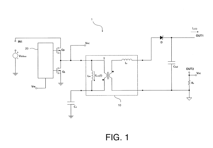
Figure 1 illustrates an embodiment of an isolated switching converter circuit
according to the present invention, denoted in its entirety by reference
numeral 1, and which will be referred to for the sake of brevity in the
following
as the converter circuit 1.
The converter circuit 1 includes-at least an input terminal IN1, particularly
suitable, in use, for connecting to an electric voltage source, in particular
a
continuous voltage source VDCbus.
The converter circuit 1 includes a pair of coupled inductors 10, represented
by the equivalent of a double-bipolar model which comprises an ideal
transformer T, a magnetising inductance Lm and a parasitic inductance L.
The circuit converter 1 also includes a pair of field effect transistors,
preferably a pair of MOSFET OH, QL, still more preferably a pair of MOSFET
with n channels.
The circuit converter 1 further includes a diode D, a pair of capacitors Cn
and
Cled and a first output terminal OUT1, particularly suitable in use for
connecting to an electrical load, preferably a light source, still more
preferably
a LED light source.
The first pole of the pair of coupled inductors 10 is connected to both the
MOSFET OH, QL, the second pole of the pair of coupled inductors 10 is
connected to the earth of the continuous voltage source via the capacitor Cni,
i.e. the capacitor of the unloaded output.
CA 03021540 2018-10-18
WO 2017/187309 PCT/IB2017/052314
6
The capacitor Cied, is connected between the third pole of the pair of coupled
inductors 10, i.e. the mass of the secondary, and the cathode of the diode D,
which coincides with the first output terminal OUT1. The diode D, i.e. the
output diode, is connected between the first output terminal OUT1 and the
fourth pole of the pair of coupled inductors.
In use, when the input terminal IN1 is connected to the continuous voltage
source VDCbus, during the on stage (Ton) only the MOSFET OH is switched on
so as to enable energy transfer from the continuous voltage source VDCbus
towards the capacitor of the unloaded output Cn and the magnetising
inductance Lm. During the off stage(Toff) the MOSFET OH switches off and
the MOSFET QL switches on and sends the diode D in conduction on the first
output terminal OUT1, so as to enable energy transfer from the capacitor of
the unloaded output Cn and from the magnetising inductance Lm to the output
capacitor Cied and the output through the ideal transformer T and the
parasitic
inductance L.
In a particularly advantageous characteristic of the present invention, the
converter circuit 1 includes a current control system in order to be able to
carry out, in use, both a power conversion and an output current control, thus
passing from a continuous voltage in input, VDcbus(t), to a controlled direct
current lied(t) in output.
In this sense, the circuit converter 1 of the present invention further
comprises an integrated control circuit (20, connected to both the MOSFET
field effect transistors, for controlling the current of the circuit converter
1,
preferably for the hysteretic control of the current of the circuit converter
1.
However, the integrated control circuit 20 alone is not sufficient for
controlling
the direct current lied(t) in output from the circuit converter 1.
In order better to understand the present invention, some of the applicant's
considerations during the course of extended experimentation are included.
The average value of the current ILm(t) which flows in the magnetising
inductance Lm, in a case in which the transformation ratio of the ideal
transformer T is one, is equal to the average value of the output current
lied(t)
leaving the first output terminal OUT1.
CA 03021540 2018-10-18
WO 2017/187309 PCT/IB2017/052314
7
However, it is necessary to consider the triangular waveform of the current
11_4) flowing in the magnetising inductance Lm. This current cannot be read
using known-type reading devices, as mentioned, the magnetising
inductance Lm is not a real component but is a part of the model of the pair
of
coupled inductors and therefore is not accessible. In order to obtain a
current
control it has even been considered to carry out the control on the average
value of the output current lied(t) which can be read by means of a measure
resistance.
The current control system of the conversion circuit 1 of the present
invention
therefore comprises a control loop 100, preferably a retroactive control loop,
and a measure resistance Rs connected to a second output terminal OUT2 of
the conversion circuit 1.
With particular reference to the embodiment illustrated in figure 2, the
control
loop 100 comprises a first input terminal VAC connected at the common node
in common to the two MOSFET OH attack QL, and a second input terminal
VDC connected to the resistance Rs. The control loop 100 further comprises a
high pass filter 22 connected to the first input terminal Vac of the control
loop
100, a low pass filter (24) connected to the high pass filter 22, a first
amplification block 26 with gain GAC connected to the low pass filter 24, and
a
summing node 28 connected to the first amplification block 26.
The control loop 100 further comprises a second amplification block 30 with
gain GAC connected to the second input terminal VDC of the control loop 100,
an optoisolator 32 connected to the second amplification block 30, a signal
decoupling stage 34 (buffer) connected to the optoisolator 32 and to the
summing node 28.
The control loop 100 lastly comprises an output terminal VFB connected to
the integrated control circuit 20.
According to the present invention, in order to carry out a power conversion
passing from a continuous voltage value, VDcbus(t), at a controlled direct
current value lied(t) with the above-described circuit, an indirect
reconstruction
method of the waveform that would be obtained if it were possible to carry
out the measurement of the current ILm(t) flowing in the magnetising
CA 03021540 2018-10-18
WO 2017/187309 PCT/IB2017/052314
8
inductance Lm is necessary.
With reference to figures 4a to 4f, the current ILm(t) can be broken down into
two components, a direct component and a frequency component. The direct
component corresponds to the average value of the current lied in output from
the first output terminal OUT1, while the component in frequency is a
triangular wave having a nil average value, and which during the on stage
(Ton) has a positive slope with a coefficient of
VDCbus ¨ Vied
Lm
and during the off stage (Toff) it has a negative slope with a coefficient of
Vied
_
Lm
The method therefore comprises steps of:
- measuring a voltage VAC(t) on the terminal VAC connected to the node in
common with the two MOSFET OH and QL (square waveform),
- subtracting, from the voltage measurement (VAc(t)), the mean value via
the high pass filter (22) with a much greater time constant (-GI-1p) than the
switching period (Ton + Toff),
- filtering, via the low pass filter (24), the waveform in output from the
high
pass filter (22) with a much greater time constant (-GI-1p) than the switching
period (Ton + Toff), obtaining a triangular waveform.
- amplifying, via the first amplification block 26 with a gain GAC, the
waveform in output from the low pass filter (24), and
- sending, to the summing node 28, the waveform V'Ac(t) in output from
the first amplification block 26.
The waveform V'Ac(t) will have a triangular progression, exactly like the
frequency component of the current flowing in the magnetising inductance Lm
and the slopes during the on and off stage will respectively be first positive
and then negative with the following coefficients.
CA 03021540 2018-10-18
WO 2017/187309 PCT/IB2017/052314
9
(VDCbus ¨ Vled)
_________________________________________ x GAc
TLP
and
(Vled
¨) x GAc
TLP
The method therefore comprises steps of:
- measuring a current in output from the converter circuit 1 by measuring
the voltage VDc(t) at the heads of the measuring resistance Rs,
- amplifying and filtering the measure of the voltage (VDc(t) via the
second amplification block 30 with a gain GDC,
- transmitting the waveform V'Dc(t) = !LED x Rs X GDC in output from the
amplification block 30 to the summing node 28 via the optoisolator 32.
As in output from the summing node 28 by predetermined dimensioning of
the multiplication factors GDC and GAc,it is possible to obtain a waveform
VFB(t) = rAc(t) + V'Dc(t) identical to that which would be obtained by direct
measuring of the current flowing in the magnetising inductance Lm, it is
possible to control the average value of the output magnitude lied(t) of the
converter circuit 1 of the present invention in a hysteretic way by using the
integrated control circuit 20, and it is possible to use the voltage VFB(t) as
a
control magnitude by following the hysteretic control methods of known type.
In an embodiment of the present invention, the above-described method can
also comprise a step of decoupling the result of the amplification and the
filtering of the voltage measurement VDc(t) in output from the optoisolator 32
via the signal decoupling stage of the 34 before sending it to the summing
node 28.
In a further aspect of the present invention the switching converter circuit
can
be used in a continuous conduction mode (CCM). With this solution the RMS
values of the current can be considerably reduced, therefore improving the
parameters of electromagnetic inference ("EMI").
As indicated in the preamble of the present description, the converter 1
circuit
of the present invention is particularly suited to being used as a second
stage
of power conversion, or output stage, of a power supply for LED light
sources. With particular reference to figure 3, a power supply 40 for LED
light
CA 03021540 2018-10-18
WO 2017/187309 PCT/IB2017/052314
sources comprises a first EMI filter stage 50, a second active rephasing
stage 60, and a circuit converter 1 according to the present invention. The
power supply 40 is connected to a LED light source 70.
In greater detail, the EMI filter stage 50 is a passive filter that enables
the
electronic devices to respond to the rules of electromagnetic compatibility,
and includes a filter TC composed of a common mode choke coil Lchoke and a
pair of capacitors Cx in class X.
The active rephasing stage 60 carries out the power conversion from the
sinusoidal mode (AC) to the direct mode (DC), while keeping the power
factors (PF) and the total harmonic distortion (THD) close to the ideal
values.
Generally this is a BOOST converter able to produce a controlled voltage
continuous output at about 400 Volts. The active rephasing stage 60 includes
a complete diode bridge 62 for rectification of the grid voltage (PNT), a
first
capacitor Cboost for the filtering of the high-frequency components generated
during the conversion, a MOSFET Qboost which, controlled by an integrated
circuit ICboost, enables energy accumulation in an inductor Lboost during the
on
phase (Tonboost), i.e with the MOSFET Qboost closed.
During the off stage (Toffboost), i.e. with the MOSFET Qboost open, the energy
is
transferred onto a second capacitor CELboost and onto the output via a diode
Dboost. Note that the integrated circuit ICboost is able to control this
energy
transfer so that it passes from the sinusoidal mode to the direct mode while
maintaining the phase shift between current absorbed from the grid and the
grid voltage.
The LED light source 70, which constitutes the electrical load of the power
supply 40, comprises one or more LEDs 72 and requires a low ripple direct
current.
In a further aspect of the present invention the value of the controlled
magnitude in output, i.e. the current, can be changed by acting on the
on
switching times ratio ( T ). With this solution it is possible to
considerably
Ton+T 0 f f
improve the voltage dynamic in output.
Though the invention has been developed with particular regard, though not
limitedly, to a switching converter circuit, i.e. a switching converter,
CA 03021540 2018-10-18
WO 2017/187309 PCT/IB2017/052314
11
particularly suitable for use as a second stage of power conversion, or output
stage, of a transformer for LED light sources, a technical expert in the
sector
might easily use the converter circuit 1 of the present invention in different
electronic devices, such as in power supplies for different electrical loads,
for
example for electrical and/or electronic apparatus different to a light source
and/or a LED light source.
All the details can be substituted by other technically-equivalent elements.
Likewise, the materials used, as well as the forms and dimensions thereof,
can be any according to needs without for this reason forsaking the scope of
protection of the following claims.