Note: Descriptions are shown in the official language in which they were submitted.
287237-5
MANGANESE-DOPED PHOSPHOR MATERIALS FOR HIGH POWER DENSITY
APPLICATIONS
BACKGROUND
[0002] Light emitting devices such as light emitting diodes (LEDs) and laser
diodes (LDs) are
well known solid state lighting elements capable of generating light upon
application of a
sufficient voltage. These light emitting devices are commonly used in various
lighting and
illuminating applications such as general lighting, automotive lighting,
displays, and projection
applications.
[0003] It is often desirable to incorporate phosphor into these light emitting
devices to enhance
the emitted radiation in a particular wavelength region and/or to convert at
least some of
radiation to another wavelength region. Generally, white light can be
generated with blue-
emitting devices and one or more of yellow, red, and green emitting phosphors.
For example,
red-emitting phosphors based on complex fluoride materials activated by
manganese (Me),
such as those described in US 7,358,542, US 7,497,973, and US 7,648,649, can
be utilized in
combination with yellow/green emitting phosphors such as YAG:Ce or other
garnet
compositions with a blue-emitting device, to achieve warni white light
(CCTs<5000 K on the
blackbody locus, color rendering index (CRI >80).
[0004] Typically, phosphor materials in particulate form are dispersed in a
resin such as silicone
to form a layer for use in lighting devices. However, such conventional
phosphor materials (in
layers) may exhibit low thennal conductivities and thermal quenching (a
decrease in internal
quantum efficiency with temperature). It has been challenging using
conventional phosphor
materials in high power density lighting devices because the phosphor
materials may deteriorate
and damage (for example, decompose) under high power density light. For
example, as the
1
Date Recue/Date Received 2023-05-25
CA 03022990 2018-11-01
WO 2017/196779 PCT/US2017/031654
power density of excitation light increases, the heat generated by the device
increases that is
detrimental for the phosphor materials. The use of conventional phosphor
materials in such high
power density lighting devices limits the applicable device power and
performance.
[0005] Therefore, there remains a need for phosphor materials that facilitate
the manufacturing
of high power density lighting devices that include phosphor materials, and
provide improved
performance.
BRIEF DESCRIPTION
[0006] Briefly, in one aspect, a lighting apparatus includes a semiconductor
light source capable
of producing blue light of high power density, the semiconductor light source
radiationally
coupled to a phosphor of formula I in a monolithic form selected from single
crystal and ceramic,
Ax (M, Mn)Fy
(I)
wherein A is Li, Na, K, Rb, Cs, or a combination thereof, M is Si, Ge, Sn, Ti,
Zr, Al, Ga, In, Sc,
Hf, Y, La, Nb, Ta, Bi, Gd, or a combination thereof, x is an absolute value of
a charge of an
[MFy] ion; and y is 5, 6, or 7.
[0007] In one aspect, a backlight apparatus includes a semiconductor light
source capable of
producing blue light of high power density, the semiconductor light source
radiationally coupled
to a phosphor of formula I in a monolithic form selected from single crystal
and ceramic.
[0008] In one aspect, a lighting apparatus includes a semiconductor light
source capable of
producing blue light of high power density, the semiconductor light source
radiationally coupled
to a phosphor wheel including a phosphor of formula I in a composite form.
[0009] In one aspect, a backlight apparatus includes a semiconductor light
source capable of
producing blue light of high power density, the semiconductor light source
radiationally coupled
to a phosphor wheel including a phosphor of formula I in a composite form.
DRAWINGS
2
CA 03022990 2018-11-01
WO 2017/196779 PCT/US2017/031654
[0010] These and other features, aspects, and advantages of the present
invention will become
better understood when the following detailed description is read with
reference to the
accompanying drawing in which like characters represent like parts throughout
the drawings,
wherein:
[0011] FIG. 1 is a schematic cross-sectional view of a lighting apparatus, in
accordance with
some embodiments of the present disclosure;
[0012] FIG. 2 is a schematic perspective view of a surface-mounted device
(SMD), in
accordance with some embodiments of the present disclosure;
[0013] FIG. 3 is a schematic view of a lighting apparatus including a phosphor
wheel, in
accordance with some embodiments of the present disclosure; and
[0014] FIG. 4 is a schematic of a phosphor wheel, in accordance with some
embodiments of the
present disclosure.
DETAILED DESCRIPTION
[0015] In the following specification and the claims, the singular forms "a",
"an" and "the"
include plural referents unless the context clearly dictates otherwise. As
used herein, the term
"or" is not meant to be exclusive and refers to at least one of the referenced
components being
present and includes instances in which a combination of the referenced
components may be
present, unless the context clearly dictates otherwise.
[0016] Approximating language, as used herein throughout the specification and
claims, may be
applied to modify any quantitative representation that could peimissibly vary
without resulting in
a change in the basic function to which it is related. Accordingly, a value
modified by a term or
terms, such as "about" and "substantially" is not limited to the precise value
specified. In some
instances, the approximating language may correspond to the precision of an
instrument for
measuring the value.
[0017] As used herein, the terms "phosphor", "phosphor composition", and
"phosphor material"
may be used to denote both a single phosphor as well as blends of two or more
phosphors.
3
CA 03022990 2018-11-01
WO 2017/196779 PCT/US2017/031654
[0018] As used herein, the term "disposed on" refers to layers or materials
disposed directly in
contact with each other or indirectly by having intervening layers or features
there between,
unless otherwise specifically indicated.
[0019] As used herein, the term "monolithic form" refers to a single crystal
or a single block or
piece of a material. In some embodiments, a phosphor of formula I in a
monolithic form includes
a single block or piece formed of sintered particles stuck together to form a
rigid agglomerate of
particle of the phosphor of formula I. The term "phosphor of formula I in a
monolithic form"
may also be referred to as "monolithic form" or "monolith" of the phosphor of
formula I, and
these terms are used interchangeably throughout the specification.
[0020] Some embodiments are directed to a lighting apparatus that includes a
semiconductor
light source capable of producing blue light of high power density that is
radiationally coupled to
a phosphor of formula Tin a monolithic form selected from single crystal and
ceramic. The
semiconductor light source may be a light-emitting diode (LED), a laser diode
(LD) or a hybrid
of LED and LD. In some embodiments, a blue light flux of the semiconductor
light source is
higher than 25 W/cm2. In some embodiments, a blue light flux of the
semiconductor light source
is higher than 40 W/cm2. Radiationally coupled means that radiation from the
semiconductor
light source is transmitted to the phosphor of formula I that emits radiation
of a different
wavelength. A combination of the light from the semiconductor light source and
the light
emitted from the phosphor of formula I may be used to produce a desired color
emission or white
light. The phosphor of formula Tin the monolithic form may be disposed on the
semiconductor
light source or located remotely from the semiconductor light source. In some
embodiments, the
monolithic form of the phosphor of formula I is a single crystal. In some
embodiments, the
monolithic form of the phosphor of formula I is a ceramic.
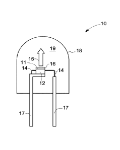
[0021] FIG,1 illustrates a lighting apparatus 10 according to some embodiments
of the present
disclosure. The lighting apparatus 10 includes a light emitting diode (LED)
chip 12, and leads 14
electrically attached to the LED chip 12. The leads 14 may be thin wires
supported by a thicker
lead frame(s) 17 or the leads may be self-supported electrodes and the lead
frame may be
omitted. The leads 14 provide current to LED chip 12 and thus cause it to emit
radiation. The
LED chip 12 may be based on any organic or inorganic semiconductor, for
example a
semiconductor of formula IniGajAlkN (where 0<; 0<j; 0<k and i +j + k =1)
having an emission
4
CA 03022990 2018-11-01
WO 2017/196779 PCT/US2017/031654
wavelength greater than about 420 nanometers (nm) and less than about 480 nm.
More
particularly, the LED chip 12 may be a blue emitting LED having a peak
emission wavelength
from about 440 nm to about 460 nm. In the lighting apparatus 10, a monolith 16
that includes the
monolithic form of the phosphor of formula I, is disposed on a surface 11 of
the LED chip 12 i.e.,
radiationally coupled to the LED chip 12. The monolith of the phosphor of
formula I can be
disposed on the LED 12 by placing or gluing the monolith 16 to the surface 11
of the LED chip
12. The light emitted by the LED chip 12 mixes with the light emitted by the
monolith 16 to
produce desired emission (indicated by arrow 15).
[0022] With continued reference to FIG. 1, the LED chip 12 may be encapsulated
within an
envelope 18, which encloses the LED chip 12 and an encapsulant material
disposed in a portion
19 of the lighting apparatus 10. The envelope 18 may be, for example, glass or
plastic. The LED
chip 12 may be enclosed by the encapsulant material. The encapsulant material
may be a low
temperature glass, or a polymer or resin known in the art, for example, an
epoxy, silicone, epoxy-
silicone, acrylate or a combination thereof. In an alternative embodiment, the
lighting apparatus
may only include the encapsulant material without the outer envelope 18.
[0023] In some other embodiments, the monolith 16 may be disposed onto a
surface of the
envelope 18, instead of being disposed on the LED chip 12. Moreover, in some
embodiments,
the lighting apparatus 10 may include a plurality of LED chips. These various
structures
discussed with respect to FIG. 1 may be combined, with the monolith 16 located
in any one or
more locations or in any other suitable location, such as separately from the
envelope 18 or
integrated into the LED chip 12. Further, one or more additional luminescent
materials
(described below) such as phosphors or mixtures of phosphors or other
materials, may be used in
different parts of the lighting apparatus 10, for example disposed on or below
the monolith 16 or
any other location in the lighting apparatus 10.
[0024] Some embodiments include a backlight apparatus that includes a surface
mounted device
(SMD) type light emitting diode 50, e.g. as illustrated in FIG. 2. This SMD is
a "side-emitting
type" and has a light-emitting window 52 on a protruding portion of a light
guiding member 54.
An SMD package may comprise an LED chip as defined above, and a phosphor of
formula I in a
monolithic foiin as described above.
5
CA 03022990 2018-11-01
WO 2017/196779 PCT/US2017/031654
[0025] The phosphor of formula I is a manganese (Mn4 ) doped complex fluoride.
Complex
fluorides have a host lattice containing one coordination center, surrounded
by fluoride ions
acting as ligands, and charge-compensated by counter ions (A) as required. For
example, in
K2[SiF6], the coordination center is Si and the counter ion is K. Complex
fluorides are generally
represented as a combination of simple, binary fluorides. The square brackets
in the chemical
formula for the complex fluorides (occasionally omitted for simplicity)
indicate that the complex
ion present in that particular complex fluoride is a new chemical species,
different from the
simple fluoride ion. In the phosphor of formula I, the Mn4+ dopant or
activator acts as an
additional coordination center, substituting a part of the coordination
center, for example, Si,
forming a luminescent center. The manganese doped phosphor of formula I:
A2[(M, Mn)F6] may
also be represented as A2[MF6]:Mn4+. The host lattice (including the counter
ions) may further
modify the excitation and emission properties of the activator ion.
[0026] The counter ion A in formula I is Li, Na, K, Rb, Cs, or a combination
thereof, and y is 6.
In certain embodiments, A is Na, K, Rb, or a combination thereof. The
coordination center M in
formula I is an element selected from the group consisting of Si, Ge, Ti, Zr,
I-If, Sn, Al, Ga, In,
Sc, Y, Bi, La, Gd, Nb, Ta, and combinations thereof. In certain embodiments, M
is Si, Ge, Ti, or
a combination thereof In some embodiments, A is K and M is Si. Examples of the
phosphors of
formula I include K2[SiF6]:Mn4+, K2[TiF6]:Mn4+, K2[SnF6]:Mn4+, Cs2[TiF6]:Mn4+,
Rb2[TiF6]:Mn4+, Cs2[SiF6]:Mn4+, Rb2[SiF6]:Mn4+, Na2[TiF6]:Mn4 ,
Na2[ZrF6]:Mn4+,
K3[ZrF7]:Mn4+, K3[BiF6]:Mn4+, K3[YF6]:Mre+, K3[LaF6]:Mn4+, K3[GdF6]:Mn4+,
K2[NbF7]:Mn4+
and K2[TaF7]:Mn4 . In certain embodiments, the phosphor of formula I is
K2[SiF6]:Mn4 .
[0027] Other manganese doped phosphors that may be used in a lighting
apparatus as described
herein include:
(A) A2[MF5]:Mn4+, where A is selected from Li, Na, K, Rb, Cs, and combinations
thereof; and where M is selected from Al, Ga, In, and combinations thereof;
(B) A3[MF6]:Mn4+, where A is selected from Li, Na, K, Rb, Cs, and combinations
thereof; and where M is selected from Al, Ga, In, and combinations thereof;
(C) Zn2[MF7]:Mn4+, where M is selected from Al, Ga, In, and combinations
thereof;
6
CA 03022990 2018-11-01
WO 2017/196779 PCT/US2017/031654
(D) A[In2F7]:Mn4 where A is selected from Li, Na, K, Rb, Cs, and combinations
thereof;
(E) E[MF6]:Mn4 , where E is selected from Mg, Ca, Sr, Ba, Zn, and combinations
thereof; and where M is selected from Ge, Si, Sn, Ti, Zr, and combinations
thereof;
(F) Ba0.65Zro.35F2.7o:Mn4 ; and
(G) A3[ZrF7]:Mn4+ where A is selected from Li, Na, K, Rb, Cs, and combinations
thereof.
[0028] The amount of manganese in the phosphor of formula I as described
herein, may range
from about 1.2 mol percent (mol%) (about 0.3 weight percent (wt%)) to about
16.5 mol% (about
4 wt%). In some embodiments, the amount of manganese may range from about 2
mol% (about
0.5 wt%) to 13.4 mol% (about 3.3wt%), or from about 2 mol% to 12.2 mol% (about
3 wt%), or
from about 2 mol% to 11.2 mol% (about 2.76 wt%), or or from about 2 mol% to
about 10 mol%
(about 2.5 wt%), or from about 2 mol% to 5.5 mol% (about 1.4 wt%), or from
about 2 mol% to
about 3.0 mol% (about 0.75 wt%).
[0029] In some embodiments, the monolithic form of the phosphor of formula I
includes a single
crystal. That is, the monolithic form includes the phosphor of formula I in
single crystal form. A
single crystal may be formed by combining the phosphor of formula I in powder
form and a flux
material, firing the combination at a temperature above a eutectic temperature
of the combination
to form a melt, and cooling the melt to form the phosphor of formula I in the
single crystal foi in.
The flux material may be a fluoride, chloride or bromide of Na, K, Rb, Cs, or
a combination
thereof, Examples of suitable flux materials include KF, KHF2, KC1, KBr, NaF,
RbF, RbHF2,
CsF, CsHF2, and combinations thereof.
[0030] Another method for forming a single crystal form of the phosphor of
formula I includes
combining a compound of formula II, a source of manganese and the flux
material, firing the
combination at a temperature above a eutectic temperature of the combination
to form a melt, and
cooling the melt to form the phosphor of formula I in single crystal form,
7
CA 03022990 2018-11-01
WO 2017/196779 PCT/US2017/031654
AxMFy
wherein A is Li, Na, K, Rb, Cs or a combination thereof, M is Si, Ge, Sn, Ti,
Zr, Al, Ga, In, Sc,
Hf, Y, La, Nb, Ta, Bi, Gd or a combination thereof, x is an absolute value of
a charge of an
[MFy] ion; and y is 5, 6, or 7.
[0031] In some embodiments, in the compound of formula II, A includes K, Na or
a combination
thereof and M includes Si, Ge, Ti or a combination thereof. In certain
embodiments, A is K and
M is Si. Suitable examples of the compounds of formula II include, but are not
limited to,
K2SiF6, K2TiF6, K2ZrF6, K2SnF6, K3ZrF7, K3LnF6, K3YF6, K2NbF7, K2TaF7,
Na2SiF6, Na2TiF6,
Na2SnF6, Na2ZrF6, LiKSiF6, RbKLiAlF6 or a combination thereof. In certain
embodiments, the
compound of formula II is K2SiF6. The source of manganese may include a
compound selected
from the group consisting of MnF2, MnF3, MnF4, K2MnF4, KMnF4, K2MnFo, K2MnF6,
K3Mn2F7,
K3MnF4, K2MnF5 and combinations thereof.
[0032] The amount of flux material should be such as that suppresses the
decomposition of the
compound of formula II, for example decomposition of K2SiF6 into 21(F and
SiF4. In some
embodiments, the amount of the flux material is in a range from about 30 mol%
to about 70
mol% in the combination. The firing of the combination may be carried out at a
temperature
above the eutectic temperature of the combination in an inert or oxidizing
atmosphere. In some
embodiments, the firing temperature is a temperature higher than 650 degrees
Celsius for
example, in a range from about 650 degrees Celsius to the melting point of the
combination. On
firing, the combination melts and a melt is obtained thereby. The melt is then
cooled to grow a
single crystal. The cooling may be carried out at a slow cooling rate (for
example, < 10
degrees/hour) to grow a single crystal. A single crystal ingot of the phosphor
of formula I may
be obtained thereby. The single crystal ingot can be cut in a desired shape
and size for example,
a plate or disc-shaped single crystal to be used as the monolith 16 (FIG. 1).
[0033] In some embodiments, the monolithic form of the phosphor of formula I
includes ceramic
i.e., a sintered ceramic form of the phosphor of formula I. A sintered ceramic
is generally
obtained by forming a greenbody including powder(s) of one or more desired
ceramic
constituents, and then sinter the greenbody until the surface of the ceramic
particles begin to
8
CA 03022990 2018-11-01
WO 2017/196779 PCT/US2017/031654
soften and melt. The partially melted particles stick together to form a rigid
agglomerate of
particles i.e., a strong and dense sintered ceramic. A greenbody is an object
whose main
constituent is weakly bound ceramic material, usually in the form of bonded
powder before it has
been sintered or fired.
[0034] In some embodiments, the sintered ceramic is formed by making a
greenbody including
the phosphor of formula I and annealing the greenbody at a temperature up to
the melting
temperature of the phosphor of formula I or the eutectic temperature of a
combination of
materials used to make the greenbody. In some embodiments, a flux material as
described above
may be added to the phosphor of formula Ito form a greenbody. In some
embodiments, the
greenbody is annealed at a temperature in a range from about 600 degrees
Celsius to about the
melting point of the combination.
[0035] In some embodiments, the sintered ceramic is formed by combining the
powders of the
compound of formula II, the source of manganese and the flux material, forming
a greenbody of
the combination and annealing the greenbody at a temperature up to the
eutectic temperature of
the combination. The greenbody may be formed by pressing the constituent or
the combination
of constituents using a compression method such as isostatic pressing. The
greenbody may be
annealed in an inert or oxidizing atmosphere. In some embodiments, the green-
body is annealed
at a temperature in a range from about 600 degrees Celsius to the melting
temperature of the
combination. In some instances, the resulting sintered ceramic including the
phosphor of
formula I is then obtained that includes closely packed, dense sintered
particles.
[0036] In some embodiments, a lighting apparatus includes a semiconductor
light source capable
of producing blue light of high power density, that is radiationally coupled
to a phosphor wheel
including a phosphor of formula I. In some embodiments, the phosphor wheel
includes the
phosphor of formula Tin a monolithic form selected from single crystal and
ceramic. In some
embodiments, the phosphor wheel includes the phosphor of formula I in a
composite form. The
semiconductor light source may be a light-emitting diode (LED), a laser diode
(LD) or a hybrid
of LED and LD. In some embodiments, a blue light flux of the semiconductor
light source is
higher than 25 W/cm2. In some embodiments, a blue light flux of the
semiconductor light source
is higher than 40 W/cm2.
9
CA 03022990 2018-11-01
WO 2017/196779 PCT/US2017/031654
[0037] FIG. 3 illustrates a schematic of a lighting apparatus 20, in some
embodiments. The
lighting apparatus 20 includes a semiconductor light source 22 for example, a
LED or a LD, an
optical assembly 24 and a phosphor wheel 30. The semiconductor light source 22
is capable of
producing blue light of high power density in a wavelength range from about
420 nm to about
480 nm. In some embodiments, the semiconductor light source 22 produces blue
light of high
power density in a wavelength range from about 440 nm to about 460 nm. The
optical assembly
24 includes one or more optical elements such as mirrors, lenses and filters.
[0038] A phosphor wheel includes a plurality of spatial segments including at
least one spatial
segment having a substance that emits a light output characterized by a color
or wavelength when
the at least one spatial segment is illuminated by a suitable light source.
Each spatial segment
may include a different phosphor. For example, individual spatial segment
produces red or green
light. In some embodiments of the present disclosure, the red phosphor may be
a phosphor of
formula I or a red quantum dot material, and the green phosphor may be a green
quantum dot
material, a garnet activated with Ce3,13-SiAlON, or a combination thereof In
some
embodiments, at least one spatial segment includes the phosphor of formula Tin
the monolithic
form as described above. In some other embodiments, at least one spatial
segment includes the
phosphor of formula Tin a composite form.
[0039] FIG. 4 shows a schematic of a phosphor wheel 30, in some embodiments.
The phosphor
wheel 30 includes a core region 32 and a rim region 34 that is far from the
center 31 of the
phosphor wheel 30 and concentric with the core region 32. The core region 34
includes a
circular metal disk. The rim region 34 may include three concentric spatial
segments 36, 37, 38
on a first side 40 of the phosphor wheel 30. At least one spatial segment, for
example, the spatial
segment 36 includes the phosphor of formula I. In some embodiments, the
spatial segment 36
includes the phosphor of formula I in the monolithic form as described above.
In some other
embodiments, the phosphor of formula I in a composite form as described above.
One or both
spatial segments (37, 38) may include an additional luminescent material
(described below). In
some embodiments, at least one spatial segment 37 or 38 may be a transmission
segment in the
form of a slit. The additional luminescent materials may be included in the
one or more spatial
segments (37, 38) in form of layers, sheets, plate-like pieces, monolith,
composite etc. In some
instances, the one or more spatial segments (37, 38) may include materials
other than phosphors.
CA 03022990 2018-11-01
WO 2017/196779 PCT/US2017/031654
For example, the one or more spatial segments (37, 38) may include dichroic
filters, absorption
filters, interference filters, transparent regions with no color modifying
properties, etc. The
spatial segments 36, 37, 38 of the phosphor wheel 30 can be of same or
different sizes and/or
shapes. The phosphor wheel 30 may also include multiple separated spatial
segments that have
the same phosphor. The phosphor wheel 30 is rotatable about its axis 33 to
expose different
spatial segments (36, 37, 38) or different portions of the spatial segments of
the phosphor wheel
30 to a light from the semiconductor light source 22.
[0040] In some embodiments, the composite form of the phosphor of formula I is
a glass-
phosphor composite. The glass-phosphor composite may be obtained by mixing a
glass and the
phosphor of formula I, subjecting the mixture to a uniaxial compression so as
to have a disc or
plate form of the mixture and firing the compressed mixture (disc or plate) up
to the melt point of
the glass. Suitable glass materials include low melting point glasses as
described in
JP200739303.
[0041] In some embodiments, the composite form of the phosphor of formula I is
a polymer-
phosphor composite. The polymer-phosphor composite may be obtained by mixing a
polymer
and the phosphor of formula Ito form a slurry, and applying the slurry on the
spatial segment 36
of the phosphor wheel 30 to form a layer. Examples of suitable polymers
include epoxies,
silicones, epoxy-silicones, acrylates and combinations thereof.
[0042] Referring to FIG. 3 again, radiation from the semiconductor light
source 22 strikes the
optical assembly 24 that focuses the radiation onto the first side 40 of the
phosphor wheel 30.
The light emitted by the phosphor wheel 30 may be directed to a collector (not
shown in FIG. 3).
The collector may include one or more lenses or other optical elements, for
example, projection
lenses that collect and transfer the light that exits the phosphor wheel 30,
to other components,
for example, a screen for display. The phosphor wheel 30 may be rotated about
its axis 33 for
moving the different spatial segments 36, 37, 38 with respect to the light
from the semiconductor
light source 22 to produce different color light. An actuator or motor (not
shown in figures) can
be used to move as well as control the speed of the phosphor wheel 30.
[0043] In certain embodiments, the phosphor wheel 30 is illuminated on the
first side 40 and
light is emitted from a second side 41 and is directed to a collector that is
placed in front of the
11
CA 03022990 2018-11-01
WO 2017/196779 PCT/US2017/031654
second side 41 of the phosphor wheel 30. In some embodiments, the phosphor
wheel 30 is
illuminated on the first side 40 and light is emitted from the first side 40
and is reflected to direct
it to a collector placed at a suitable position. In some other embodiments,
the phosphor wheel 30
can be illuminated on both sides (40, 41).
[0044] Although the phosphor wheel 30 shown in figures 3 and 4 includes
spatial segments at the
rim region 34, a phosphor wheel may have different configurations and may be
configured to
move in a different manner other than being rotated.
[0045] In some embodiments, the phosphor of formula I may be treated as
described in U.S.
Patents 8,252,613 and 8,906,724 to enhance performance and color stability
properties prior to or
after forming the monolithic form or the composite form as described above.
The treatment
process includes contacting the phosphor of formula I at an elevated
temperature with a fluorine-
containing oxidizing agent in gaseous form. In some embodiments, the single
crystal of the
phosphor of formula I is treated using the treatment process.
[0046] Suitable examples of additional luminescent materials for use in a
phosphor wheel and/or
a lighting apparatus with the phosphor of formula I may include, but are not
limited to:
((Sri_z (Ca, Ba, Mg, Zn)z)14.-i-w)( Li, Na, K, Rb)wCex)3(All-ySiy)04-Ey+3(x-
w)F1-y-3(x-w), 0<x).10,
0y).5, Oz). 5, Ovtlx; (Ca, Ce)3Sc2Si3012(CaSiG);
(Sr,Ca,Ba)3Ali_xSix04+xFi_x:Ce3+
(SASOF)); (Ba,Sr,Ca)5(PO4)3(CI,F,Br,OH):Eu2+,Mn2+; (Ba,Sr,Ca)BP05:Eu2+,Mn2+;
(Sr,Ca)10(PO4)6*vB203:Eu2+ (wherein 0<v51);
Sr2Si308*2SrC12:Eu2+;(Ca,Sr,Ba)3MgSi208:Eu2+,Mn2+; BaA18013:Eu2+;
2SrO*0.84P205*0.16B203:Eu2+; (Ba,Sr,Ca)MgA110017:Eu2+,Mn2+;
(Ba,Sr,Ca)A1204:Eu2+;
(Y,Gd,Lu,Sc,La)B03:Ce3+,Tb3+; ZnS:Cu+,C1-; ZnS:Cu+,A13+; ZnS:Ag+,CI-;
ZnS:Ag+,A13+;
(Ba,Sr,Ca)2Sil_04-2:Eu2+ (wherein -0.2550.2); (Ba,Sr,Ca)2(Mg,Zn)Si207:Eu2+;
(Sr,Ca,Ba)(AI,Ga,ln)2S4:Eu2+; (Y,Gd,Tb,La,Sm,Pr,Lu)3(AI,Ga)5_0,012-3/2a:Ce3+
(wherein 05cc50.5);
(Ca,Sr)8(Mg,Zn)(Si0.4)4C12:Eu2+,Mn2+; Na2Gd2B207:Ce3+,Tb3+;
(Sr,Ca,Ba,Mg,Zn)2P207:Eu2+,Mn2+;
(Gd,Y,Lu,La)203:Eu3+,Bi3+; (Gd,Y,Lu,La)202S:Eu3+,Bi3+;
(Gd,Y,Lu,La)VO4:Eu3+,Bi3+;
(Ca,Sr)S:Eu2+,Ce3+; SrY2S4:Eu2+; CaLa2S4:Ce3+; (Ba,Sr,Ca)MgP207:Eu2+,Mn2+;
(Y,Lu)2W06:Eu3+,Mo6+; (Ba,Sr,Ca)pSiyNI,:Eu2+ (wherein 213+4y=3 );
(Ba,Sr,Ca)2Si5_,A1,N8_õOx:Eu2+
(wherein 05)(52); Ca3(S104)C12:Eu2+; (Lu,Sc,Y,Tb)2_u_vCevCal-
EuLiwMg2_wPw(Si,Ge)3_w012-u/2 (where
0.551_151, 0<v50.1, and 05w50.2); (Y,Lu,Gd)2Caq,Si4N6+TC,:Ce3+, (wherein
05950.5);
12
CA 03022990 2018-11-01
WO 2017/196779 PCT/US2017/031654
(Lu,Ca,Li,Mg,Y), a-SiAION doped with Eu2+ and/or Ce3+;
(Ca,Sr,Ba)SiO2N2:Eu2+,Ce3+; 13-
SiAION:Eu2+, 3.5MgO*0.5MgF2*Ge02:Mn4+; (Sr,Ca,Ba)AlSiN3:Eu2+;
(Sr,Ca,Ba)3Si05:Eu2+;
fCecEufAli+,Sii_cN3, (where 05c50.2, 05f50.2); Cal-h-rCenairAli-h(Mg,Zr)nSi
N3, (where 05h50.2,
05r50.2); Cal-2s-(Ces(Li,Na)8Eu(AISiN3, (where 05s50.2, 05t50.2, s+t>0); and
Cal_cy-x-(oCecy
(Li,Na)xEuAli+,-xSil_,+xN3, (where 05(350.2, 05x50.4, 05(1)50.2).
In some particular embodiments, the additional luminescent material includes a
green-emitting
material such as a garnet activated with Ce3+, 13-SiAlON, or a combination
thereof
[0047] In some embodiments, the additional luminescent material includes a
green light emitting
quantum dot (QD) material. The green light emitting QD material may include a
group II-VI
compound, a group III-V compound, a group IV-IV compound, a group IV compound,
a group I-
III-VI2 compound, or a mixture thereof Non-limiting examples of group II-VI
compounds
include CdSe, CdTe, CdS, ZnSe, ZnTe, ZnS, HgTe, HgS, HgSe, CdSeTe, CdSTe,
ZnSeS,
ZnSeTe, ZnSTe, HgSeS, HgSeTe, HgSTe, CdZnS, CdZnSe, CdZnTe, CdHgS, CdHgSe,
CdHgTe, HgZnS, HgZnSe, HgZnTe, CdZnSeS, CdZnSeTe, CdZnSTe, CdHgSeS, CdHgSeTe,
CdHgSTe, HgZnSeS, HgZnSeTe, HgZnSTe, or combinations thereof Group III-V
compounds
may be selected from the group consisting of GaN, GaP, GaAs, MN, AlP, AlAs,
InN, InP, InAs,
GaNP, GaNAs, GaPAs, AlNP, AINAs, AlPAs, InNP, InNAs, InPAs, GaAINP, GaA1NAs,
GaA1PAs, GalnNP, GalnNAs, GalnPAs, InAlNP, InAlNAs, InAlPAs, and combinations
thereof
Examples of group IV compounds include Si, Ge, SiC, and SiGe. Examples of
group I-III-V12
chalcopyrite-type compounds include CuInS2, CuInSe2, CuGaS2, CuGaSe2, AgInS2,
AgInSe2,
AgGaS2, AgGaSe2 and combinations thereof
[0048] QD materials for use as the additional luminescent material may be a
core/shell QD,
including a core, at least one shell coated on the core, and an outer coating
including one or more
ligands, preferably organic polymeric ligands. Exemplary materials for
preparing core-shell QDs
include, but are not limited to, Si, Ge, Sn, Se, Te, B, C (including diamond),
P, Co, Au, BN, BP,
BAs, MN, MP, AlAs, AlSb, GaN, GaP, GaAs, GaSb, InN, InP, InAs, InSb, AIN, AlP,
AlAs,
AlSb, GaN, GaP, GaAs, GaSb, ZnO, ZnS, ZnSe, ZnTe, CdS, CdSe, CdSeZn, CdTe,
HgS, HgSe,
HgTe, BeS, BeSe, BeTe, MgS, MgSe, MnS, MnSe, GeS, GeSe, GeTe, SnS, SnSe, SnTe,
Pb0,
PbS, PbSe, PbTe, CuF, CuCl, CuBr, CuI, Si3N4, GeN4, A1203, (Al, Ga, In)2 (S,
Se, Te)3, Al2CO3
and appropriate combinations of two or more such materials. Exemplary core-
shell QDs include,
13
CA 03022990 2018-11-01
WO 2017/196779 PCT/US2017/031654
but are not limited to, CdSe/ZnS, CdSe/CdS, CdSe/CdS/ZnS, CdSeZn/CdS/ZnS,
CdSeZn/ZnS,
InP/ZnS, PbSe/PbS, PbSe/PbS, CdTe/CdS, and CdTe/ZnS.
[0049] The QD materials typically include ligands conjugated to, cooperated
with, associated
with, or attached to their surface. In particular, the QDs may include a
coating layer comprising
ligands to protect the QDs from environmental conditions including elevated
temperatures, high
intensity light, external gasses, and moisture, control aggregation, and allow
for dispersion of the
QDs in the host binder material.
[0050] The ratio of each of the individual luminescent materials, for example
phosphor of
formula I and the additional luminescent materials may vary depending on the
characteristics of
the desired resulting light output. The relative proportions of the individual
luminescent
materials in the lighting apparatus or the phosphor wheel may be adjusted such
that when
emissions of the individual luminescent materials are blended, and employed in
a lighting
apparatus, visible light of predetermined x and y values is produced on the
chromaticity diagram
created by the International Commission on Illumination (CIE). In certain
embodiments, the
lighting apparatus emits white light. The exact identity and amount of each
luminescent material
in a lighting apparatus as described herein can be varied according to the
needs of the end user.
[0051] The lighting apparatus and/or backlight apparatus of the present
invention may be used
for general illumination and display applications. Examples include chromatic
lamps, plasma
screens, xenon excitation lamps, UV excitation marking systems, automotive
headlamps, home
and theatre projectors, laser pumped devices, point sensors, liquid crystal
display backlight units,
televisions, computer monitors, smartphones, tablet computers and other
handheld devices that
have a display including a semiconductor light source as described herein. The
list of these
applications is meant to be merely exemplary and not exhaustive.
EXAMPLES
[0052] The examples that follow are merely illustrative, and should not be
construed to be any
sort of limitation on the scope of the claimed invention.
[0053] Example 1: Procedure to form K2(Si, Mn)F6 in single crystal fol in
14
287237-5
[0054] A mixture of K2SiF6 (40 mol%) and ICBr (60 mol%) was weighed in glove
box. The
mixture (1 gram) was put in a platinum crucible and transferred to a mullite
tube furnace. The
tube furnace was purged with Ar atmosphere for 30 minutes followed by firing
at 675 degrees
Celsius for a 1 hour hold, (3 degrees Celsius up and down/Ar bubbled through
KOH). The
resulting melt was purged for 30 minutes in Ar atmosphere. The platinum
crucible, which
contained the melt, was taken out of the furnace and washed in methanol to
dissolve excess ICBr.
It was observed that the bubbler looked clean confirming no or minimal
formation of SiF4 due to
the decomposition of K2SiF6.
[0055] The washed melt was examined using X-ray diffraction (XRD). XRD results
showed that
the melt had the desired phase K2SiF6. This indicates that a single crystal of
phase K2SiF6 can be
grown if the melt point is suppressed to prevent decomposition of K2SiF6 into
2ICF and SiF4.
Using a similar procedure, IC2(Si, Mn)F6 can be grown in single crystal using
either IC2(Si,Mn)F6
or K2SiF6 and a Mn compound in the starting mixture.
[0056] Example 2: Procedure to form K2(Si, Mn)F6 in sintered ceramic form
[0057] Sintered ceramic parts of IC2(Si, Mn)F6 can be formed via HIP (Hot
isostatic pressing) of
the starting materials and/or by making a greenbody with further sintering to
produce a
transparent or translucent ceramic part. In the process, particle size may be
well controlled and
small amounts of flux material may be added to improve sintering and
densification.
[0058] While only certain features of the invention have been illustrated and
described herein,
many modifications and changes will occur to those skilled in the art. It is,
therefore, to be
understood that the disclosure is intended to cover all such modifications and
changes as fall
within the true scope of the invention.
Date Recue/Date Received 2023-05-25