Note: Descriptions are shown in the official language in which they were submitted.
CA 03024489 2018-11-16
GB030 (MP1087A)
Method for manufacturing secondary battery
Technical Field
[0001] The present invention relates to a method for manufacturing an all
solid
secondary battery.
Background Art
[0002] As a device having a power storage function, there are a secondary
battery
and a capacitor. A secondary battery is a device utilizing a chemical reaction
and is
characterized by its large capacity. The capacitor is characterized in that
charges are
accumulated while sandwiching an insulator between the electrodes, so that it
can be
charged in a short time. Examples of secondary batteries include nickel-
cadmium
batteries and lithium ion secondary batteries. As a capacitor, there are a
super
capacitor (also called an electric double layer capacitor.), a MOS capacitor
and the like.
[0003] A lithium ion secondary battery, which is a typical secondary battery,
has a
three-layer structure in which a separator is sandwiched between a positive
electrode
and a negative electrode, and these constituent elements are covered with an
electrolyte capable of flowing lithium ions. The positive electrode and the
negative
electrode are materials capable of absorbing and releasing lithium ions and
electrons.
Inside the lithium ion battery, lithium ions move between the positive
electrode and
the negative electrode via the electrolyte to perform charging and
discharging.
[0004] As a laminated structure of a solid lithium ion secondary battery, the
structure disclosed in Patent Document 1 includes a positive electrode layer
having a
positive electrode active material into which lithium ions enter and exit, a
negative
electrode layer having a negative electrode active material into which lithium
ions
enter and exits, and a positive electrode And a solid electrolyte layer
disposed between
the anode layer and the anode layer. The solid electrolyte layers of the two
adjacent
laminates are connected by an insulating layer. Furthermore, the two adjacent
laminates are laminated so that the anode layers constituting each laminate or
the
cathode layers constituting each laminate come into contact with each other.
[0005] As a secondary battery based on a new principle, Patent Document 2
discloses
a quantum battery. "Quantum battery" is a name given to the secondary battery
disclosed in Patent Document 2.
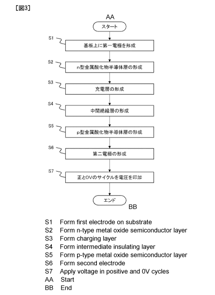
[0006] FIG. 14 is a diagram showing a cross section of the quantum battery
100. In
the quantum battery 100, a conductive first electrode 312 is formed on a
substrate, and
a charge layer 114 for charging the charge, a p-type metal oxide semiconductor
layer
116 and a second electrode 118 are stacked. The charging layer 114 is filled
with fine
particle n-type metal oxide semiconductor covered with an insulative film to
generate a
photoexcited structural change phenomenon by irradiation with ultraviolet
light,
thereby a new energy level is formed in a band gap of the n-type metal oxide
semiconductor
1
CA 03024489 2018-11-16
GB030 (MP1087A) r=kmftonas,itj
[0007] In addition, Patent Document 3 discloses a new secondary battery in
which a
function of an eleetrochromic display device and a secondary battery are
integrated
using a semiconductor. What is claimed is: 1. A semiconductor device
comprising; a
substrate; a first electrode; a porous layer made of a semiconductor metal
oxide; an
active layer comprising a composite of a semiconductor metal oxide and an
insulating
metal oxide and reversibly generating an oxidation- , An electron blocking
layer, and a
second electrode, and structurally has the same structure as the quantum
battery
shown in FIG. The active layer accumulates or releases charges by oxidation-
reduction
reaction, and is used as an electrochromic display device / secondary battery
integrated
solid-state device whose light transmittance changes in conjunction with
charge
accumulation or release.
[0008] The difference between the quantum battery disclosed in Patent Document
2
and the secondary battery disclosed in Patent Document 3 is that, in the
latter
structure, the charge layer is a composite of a semiconductor metal oxide and
an
insulating metal oxide and that no new energy level is formed within the band
gap of
the n-type metal oxide semiconductor by ultraviolet irradiation. Due to these
differences, in the latter case, the principle of charge and discharge is
based on the
reversible oxidation-reduction reaction between the semiconductor metal oxide
and the
insulating metal oxide.
[0009] In the secondary battery disclosed in Patent Document 3, the complex
oxide
thin film is changed to an active state by performing a photoexcitation
structure
change process on the complex oxide thin film, and as a photoexcited structure
change
process, a method based on ultraviolet irradiation can be used.
[0010] Processing performed after formation of the secondary battery includes
aging
treatment and conditioning treatment.
[0011] A lithium secondary battery includes an electrode body provided with a
positive electrode and a negative electrode in a battery case, the battery
case is sealed
after the nonaqueous electrolyte is injected. After the formation of a lithium
secondary
battery, a so-called aging treatment in which the lithium secondary battery is
stored at
a predetermined temperature is performed thereafter, and performs conditioning
processing for adjusting the battery to a state in which the battery can be
actually
usable by performing charging/discharging (refer to patent document 4).
[0012] Conditioning is to repeat the cycle of charging and discharging a
plurality of
times on the formed secondary battery for the purpose of stabilizing battery
performance and the like. SET (Solid Electrolyte Interphase) coating
comprising a
lithium-containing compound or the like is formed on the surface of the
negative electrode
by conditioning a lithium secondary battery using a carbonaceous material or
the like as a
negative electrode active material. Since the SET film covering the surface of
the negative
electrode hardly grows, once the state of the SEI film does not change, the
battery capacity
stabilizes at this stage.
2
CA 03024489 2018-11-16
GB030 (MP1087A) FLIZt6Tgo'DtPaSit.1
6
[0013] Patent Document 5 discloses a charge / discharge device that performs
conditioning to a quantum battery using a metal oxide semiconductor (see
Patent
Document 2). When charging and discharging of a plurality of quantum batteries
are
performed in parallel at the same time, the peak current of the power supply
increases,
and therefore, in this charging device, the quantum battery are sequentially
connected
to the power supply are switched in order that the charging and discharging of
the
plurality of quantum cells do not overlap by the switching means.
Prior art literature
Patent document
[0014]
Patent document 1: W02010/089855
Patent document 2: W02012/ 046325
Patent document 3: Japanese Patent Application Laid-Open No. 2014-032353
Patent document 4: Japanese Patent Application Laid-Open No. 2004-208440
Patent document 5: WO 2014/016900
Summary of the invention
Problem to be solved by the invention
[0015] Compared to lithium ion batteries and the like using electrolytic
solution, the
all solid state secondary battery is compact, does not ignite due to heat
generation, has
high safety but charge capacity is small, further improvement is demanded.
[0016] In addition, in order to adjust the secondary battery to a state where
it can be
actually used, aging processing and conditioning processing, which are
electrical
processing performed after the formation of the secondary battery, are
performed. As
described in the background art above, these electrical processes are
conventionally
performed in order to stabilize the initial charge function, and do not
improve
performance such as an increase in discharge capacity.
[0017] For this reason, electrical processing for increasing the discharge
capacity is
desired.
[0018] The present invention relates to electrical processing performed on a
formed
secondary battery, and by examining its electrical conditions, it is possible
to increase
the discharge capacity more than the initial discharge capacity of the
secondary
battery and to provide a manufacturing method therefor.
[0019] A method of manufacturing an oxide semiconductor secondary battery
according to one embodiment of the present invention includes the steps of
preparing a
first electrode, an n-type metal oxide semiconductor layer made of an n-type
metal
oxide semiconductor, a charging layer made of an n-type metal oxide
semiconductor
and an insulator, an intermediate insulating layer containing an insulator as
a main
component, a p-type metal oxide semiconductor layer made of a p-type metal
oxide
3
CA 03024489 2018-11-16
GB030 (MP1087A) FT.&-ZitaDU,S1,-A
semiconductor, and a second electrode are stacked in this order on the first
electrode,
and then the first unit cycle includes a first process of applying a positive
voltage
between the first electrode and the second electrode with reference to the
first
electrode and a second process of applying 0 V between the first electrode and
the
second electrode, and the first unit cycle is repeated with a predetermined
number.
[0020] In the above manufacturing method, when the first electrode is
grounded, the
value of the positive voltage applied to the second electrode in the first
process includes
at least a value equal to or higher than the charging voltage of the oxide
semiconductor
secondary battery.
[0021] In the above manufacturing method, the first process includes a process
of
holding a state in which a positive voltage is applied between the first
electrode and
the second electrode for a certain period of time, and in the second process,
a process of
maintaining a state in which 0 V is applied between the first electrode and
the second
electrode for a certain period of time.
[0022] In the above manufacturing method, in the first process, a positive
voltage
applied between the first electrode and the second electrode may be set to a
different
voltage value for each cycle.
[0023] In the above manufacturing method, in the first process, the positive
voltage
applied between the electrode and the second electrode is controlled by each
process in
order to prevent the value of the current flowing between the first electrode
and the
second electrode from exceeding the predetermined current value.
[0024] In the above manufacturing method, the positive voltage application
time for
applying the positive voltage in the first process is lengthened as the
discharge
capacity of the oxide semiconductor secondary battery increases.
[0025] In the above manufacturing method, the positive voltage application
time for
applying the positive voltage is the time until the voltage value of the oxide
semiconductor secondary battery reaches the predetermined set voltage value.
[0026] Further, in the above manufacturing method, in addition to the first
process
and the second process, a third process for measuring the discharge capacity
of the
oxide semiconductor secondary battery is included, and a third process is
executed
after the predetermined number of the first unit cycles is repeated, the
application of
the voltage is terminated when it is measured that the discharge capacity of
the oxide
semiconductor secondary battery is not less than a predetermined threshold
value.
[0027] In the manufacturing method, in addition to the first process and the
second
process, a third process for measuring a discharge capacity of the oxide
semiconductor
secondary battery and a fourth process for calculating an increase rate of the
discharge
capacity of the oxide semiconductor secondary battery at a predetermined time
interval based on the discharge capacity measured in the third process,
wherein after
repeating the first unit cycle for a predetermined number of cycles, the third
process
and the fourth process is executed, and the application of the voltage is
terminated
4
CA 03024489 2018-11-16
GB030 (MP1087A) r
4
when the increase rate of the discharge capacity is equal to or less than the
predetermined threshold value.
[0028] In the manufacturing method described above, the intermediate
insulating
layer is formed by applying a silicone oil or a silicone oil to which a
resistance
adjusting agent is added is coated on the surface of the charging layer, then
baking and
irradiating with ultraviolet rays after baking to be cured by UV curing
[0029] In the above manufacturing method, the intermediate insulating layer is
formed on the charging layer by sputtering using silicon (Si) as a target.
[0030] In the above manufacturing method, the insulator of the intermediate
insulating layer is SiOx (0 x -e5 2).
[0031] In the above manufacturing method, the p-type metal oxide semiconductor
is
nickel oxide (NiO).
[0032] Furthermore, a method for manufacturing an oxide semiconductor
secondary
battery according to one embodiment of the present invention includes: a first
electrode; an n-type metal oxide semiconductor layer formed of an n-type metal
oxide
semiconductor; and an n-type metal oxide semiconductor an intermediate
insulating
layer containing an insulator as a main component, a p-type metal oxide
semiconductor layer made of a p-type metal oxide semiconductor, and a second
electrode are stacked in this order, and then a second unit cycle is defined
by a fifth
process and a sixth process, wherein a fifth process of applying a positive
voltage
between the first electrode and the second electrode on the basis of the first
electrode
and a sixth process of applying a negative voltage between the first electrode
and the
second electrode on the basis of the first electrode, and a predetermined
number of
second unit cycles are repeated.
[0033] An oxide semiconductor secondary battery having a storage function
according to the
present invention is characterized by comprising a n-type metal oxide
semiconductor layer, a
charge composed of an n-type metal oxide and an insulator sandwiched between a
conductive first
electrode and a conductive second electrode layer. The oxide semiconductor
secondary
battery having this configuration is subjected to electrical treatment to form
a layer
containing an element of an insulating layer in a p-type metal oxide
semiconductor
between the intermediate insulating layer and the p-type metal oxide
semiconductor
layer (hereinafter referred to as a mixed layer), as a result, the discharge
capacity can
be increased.
[0034] The electrical treatment is processing of applying a positive voltage
and
applying 0 V or applying positive and negative electrodes to the second
electrode side
on the basis of the first electrode after formation of the secondary battery.
[0035] The fact that a new layer is formed at the interface between the p-type
metal
oxide semiconductor and the intermediate insulating layer by this electrical
treatment
is a result found experimentally. The new layer is a mixed layer in which a
layer is
formed as a micro interface by a substance diffused from the p-type metal
oxide
CA 03024489 2018-11-16
GB030 (MP1087A) [1:7_kIrtthOT4iJ
.6
semiconductor and the intermediate insulating layer. It is considered that the
accumulation capacity of positive charges (holes) increased due to the mixed
layer
which is a new layer, and the storage capacity increased. In addition, even in
the
charged layer formed by sintering the n-type metal oxide semiconductor and the
insulating material by electric treatment, a change such as rearrangement of
the
material occurs, and the accumulation amount of the negative charge (electron)
also
increases conceivable. Therefore, for example, the result that the discharge
capacity is
doubled after the electrical treatment is obtained.
Simple description of drawings
[0036]
FIG. 1 shows a structure of an oxide semiconductor secondary battery
manufactured
by the present invention
FIG. 2 shows a structure of an oxide semiconductor secondary battery before
and
after application of a cycle voltage of positive and 0 V
FIG. 3 is a flowchart illustrating a process of manufacturing an oxide
semiconductor
secondary battery according to the present invention
FIG. 4 shows an example of an implementation of a cycle voltage application
system
FIG. 5 shows an example of a voltage waveform of positive and 0 V
FIG. 6 shows an example of two-cycle voltage waveforms
FIG. 7 shows an example of a voltage waveform at the second electrode measured
by
a voltmeter with respect to the voltage waveform shown in FIG. 6
FIG. 8 is a flowchart illustrating a process for applying a voltage waveform
FIG. 9 is an example of a unit cycle in which the positive voltage shown in
FIG. 5 is
repeated.
FIG. 10 is a graph showing the relationship between the time and the discharge
capacity when the positive voltage shown in FIG. 9 is repeatedly applied.
FIG. 11 shows an example of positive and negative voltage waveforms.
FIG. 12 shows another example of positive and negative voltage waveforms.
FIG. 13 is a graph showing the relationship between the time and the discharge
capacity when the positive and negative voltages shown in FIG. 11 are
repeatedly
applied.
FIG. 14 is a diagram for explaining a conventional example.
System for carrying out the invention
[0037] FIG. 1 shows the structure of an oxide semiconductor secondary battery
10
manufactured according to the present invention.
[0038] In Fig. 1, the oxide semiconductor secondary battery 10 includes a
first
electrode 12, an n-type metal oxide semiconductor layer 14, a charge layer 16,
an
intermediate insulating layer 18, a mixed layer 20, a p-type metal oxide
semiconductor
6
CA 03024489 2018-11-16
GB030 (MP1087A) rjj
layer 22, and the second electrodes 24 are stacked in this order.
[0039] As the material of the first electrode 12, for example, a metal such as
chromium (Cr) or titanium (Ti) can be used. In addition, as the other metal
electrode of
the first electrode 12, a silver (Ag) alloy film containing aluminum (Al) or
the like can
also be used. Further, the first electrode 12 may have a laminated structure
in which a
plurality of metal layers are laminated. The first electrode is required to be
a material
having a low resistivity. For example, it is preferable to use a material
having a
resistivity equal to or less than 1001152 cm.
[0040] As the material of the first electrode 12, a metal foil such as copper,
aluminum,
stainless steel or the like can also be used as the substrate of the oxide
semiconductor
secondary battery 10.
[0041] As a material of the n-type metal oxide semiconductor layer 14, for
example,
an n-type metal oxide semiconductor such as titanium oxide (TiO2), zinc oxide
(Zn0),
tin oxide (Sn02) or the like can be used as a material. The n-type metal oxide
semiconductor layer 14 is formed by forming an n-type metal oxide
semiconductor on
the first electrode 12.
[0042] The charge layer 16 is composed of an n-type metal oxide semiconductor
and
an insulator. As a material of the insulator, it is preferable to use a
silicon compound
(silicone) having a main skeleton by siloxane bonding such as silicon oxide.
As the
n-type metal oxide semiconductor of the charge layer 16, an n-type metal oxide
semiconductor such as titanium oxide (TiO2), zinc oxide (Zn0), tin oxide
(Sn02) or the
like can be used. The n-type metal oxide semiconductor can be included in the
insulator as nano-sized fine particles. Instead of the n-type metal oxide
semiconductor,
a precursor of an n-type metal oxide semiconductor, for example, titanium
stearate
which is a precursor of titanium oxide can be used.
[0043] The intermediate insulating layer 18 is configured to include an
insulator or
an insulator to which a resistance adjusting agent is added. As the material
of the
insulator, silicon oxide SiO2, silicon nitride Si3N4, silicon oxide SiO. (0 x
5_ 2) and the
like can be used.
[0044] The insulation resistance value of the intermediate insulating layer 18
can be
adjusted by adding a resistance adjusting agent such as a metal, a metal
oxide, a
semiconductor material or the like to silicon oxide, silicon nitride or
silicone oil. The
fact that the insulation resistance value of the intermediate insulation layer
18, that is,
the value of the current flowing through the intermediate insulation layer 18,
affects
the discharge capacity of the oxide semiconductor secondary battery 10 is
experimentally clarified.
[0045] Therefore, it is necessary to adjust the discharge capacity of the
oxide
semiconductor secondary battery to an optimum value by adjusting the
insulation
resistance value of the intermediate insulating layer 18. For example, when
the
intermediate insulating layer 18 is formed with a thickness equal to or less
than a
7
CA 03024489 2018-11-16
GB030 (MP1087A) FftgAliSVIM
predetermined value, it may be a layer containing silicon oxide as a main
component.
However, when the intermediate insulating layer 18 is formed with a
predetermined
thickness, that is, a thickness that is equal to or greater than the thickness
at which
the discharge capacity decreases, a resistance adjusting agent such as a metal
or a
semiconductor material is added to the silicon oxide, It is necessary to lower
the
insulation resistance value and to reduce the current flowing through the
intermediate
insulating layer 18 to a predetermined value or less. That is, the
intermediate
insulating layer 18 needs to be a layer including an insulator or an insulator
to which a
resistance adjusting agent is added. As the resistance adjusting agent, a
metal, a
metal oxide, a semiconductor material, or the like can be used.
[0046] The mixed layer 20 is a layer in which a p-type metal oxide
semiconductor, a
metal, and an insulator are mixed. The state of the mixed layer 20 is a state
in which a
p-type metal oxide semiconductor and an insulator are mixed, a state in which
a metal
element constituting a p-type metal oxide semiconductor is incorporated in an
insulator, or a state in which a p-type metal oxide semiconductor, or in a
state in which
an element of an insulating material is incorporated into the insulating film.
[0047] The p-type metal oxide semiconductor layer 22 is composed of a p-type
metal
oxide semiconductor. As the material of the p-type metal oxide semiconductor,
nickel
oxide (NiO), copper aluminum oxide (CuA10 2), or the like can be used.
[0048] As the material of the second electrode 24, chromium (Cr), copper (Cu)
or the
like can be used. As another material, a silver (Ag) alloy containing aluminum
(Al) or
the like can be used.
[0049] As the second electrode 24, a transparent conductive electrode can also
be
used. For example, a tin-doped indium tin oxide (ITO) is used as the second
electrode
24) of conductive films can be used. It is necessary for the second electrode
to be a
material having a low resistivity, for example, it is preferable to use a
material having
a resistivity of 100 ilS2 = cm or less.
[0050] The structure of the oxide semiconductor secondary battery 10 according
to
the present invention has been described above. In the following description,
a method
for electrically forming the mixed layer 20 will be described. In this method,
after
laminating the first electrode 12, the n-type metal oxide semiconductor layer
14, the
charge layer 16, the intermediate insulating layer 18, the p-type metal oxide
semiconductor layer 22 and the second electrode 24 in this order, The laminate
is
placed in an environment with humidity within 35 to 65 percent. Next, there is
a method
of repeatedly applying a positive voltage and 0 V of a cycle voltage from a
voltage source between
the first electrode 12 and the second electrode 24, and a method of repeatedly
applying a positive
voltage and a negative voltage of a cycle voltage from a voltage source.
Hereinafter, a method for
electrically forming the mixed layer will be described in detail.
<Outline of Mixed Layer>
[0051] FIG. 2 shows a structure of an oxide semiconductor secondary battery 10
8
CA 03024489 2018-11-16
GB030 (MP1087A) r=(katoDWISMIti
a
before and after application of a cycle voltage of positive and 0 V.
[0052] FIG. 2 (A) shows the structure of the oxide semiconductor secondary
battery
10-1 in which the first electrode 12, the n-type metal oxide semiconductor
layer 14, the
charge layer 16, the intermediate insulating layer 18, the p-type metal oxide
semiconductor layer 22 and the second electrode 24 are laminated in this
order. That is,
FIG. 2 (A) shows the oxide semiconductor secondary battery 10-1 before forming
the
mixed layer 20.
[0053] After forming the oxide semiconductor secondary battery 10-1 having the
structure shown in FIG. 2A, a positive and 0 V cycle voltage is applied
between the
first electrode 12 and the second electrode 24 by a voltage source, and the
mixed layer
20 is formed between the intermediate insulating layer 18 and the p-type metal
oxide
semiconductor layer 22. Thereby, the oxide semiconductor secondary battery 10
shown
in FIG. 2 (B), in which the mixed layer 20 is formed, is manufactured.
Formation of the
mixed layer 20 by application of the cycle voltage is a layer found
experimentally and
the result that the discharge capacity is increased by formation of the mixed
layer 20 is
obtained.
<Detailed Description of Mixed Layer>
[0054] Hereinafter, a method of manufacturing the oxide semiconductor
secondary
battery 10 including the mixed layer 20 will be described in detail using a
flowchart.
[0055] FIG. 3 is a flowchart for explaining the manufacturing process of the
oxide
semiconductor secondary battery according to the present invention.
[0056] In step Si, a first electrode 12 is formed on a substrate (not shown).
In the
case where a conductive metal foil is used as the substrate, the metal foil
itself
becomes the first electrode 12. For example, a metal foil such as copper,
aluminum,
stainless steel or the like can be used.
[0057] The first electrode 12 can also be formed by depositing a conductive
metal
such as chromium, titanium, or titanium nitride on an insulating substrate. As
a
material of the substrate, glass or a flexible resin sheet such as polyimide
film can be
used.
[00581 As a manufacturing method of the first electrode 12, a vapor phase film
forming method such as sputtering, ion plating, electron beam vapor
deposition,
vacuum vapor deposition, chemical vapor deposition or the like can be
mentioned.
When the metal is used as the first electrode 12, it can be formed by
electrolytic plating,
electroless plating, or the like. In general, copper, copper alloy, nickel,
aluminum, silver,
gold, zinc, tin or the like can be used as the metal used for plating.
[0059] In step S2, the n-type metal oxide semiconductor layer 14 of a n-type
metal
oxide semiconductor film such as titanium oxide, tin oxide, zinc oxide or the
like is
formed on the first electrode 12.
[0060] In step S3, a charge layer 16 made of an n-type metal oxide
semiconductor and
an insulator is formed on the n-type metal oxide semiconductor layer 14.
9
CA 03024489 2018-11-16
GB030 (MP1087A) F_--iwatowisi
. . ,
-
The charging layer (16) is a mixture of a precursor of an n-type metal oxide
semiconductor
such as tin oxide or zinc oxide, silicone oil as an insulator and a solvent,
and is formed by a spin
coating method, a slit coating method, a spin coating method, a spin coating
method, a
spin coating method, or a slit coating method, and then drying and firing, the
n-type
metal oxide semiconductor layer 14. is spin-coated, the n-type
metal oxide
semiconductor layer 14 is coated on the n-type metal oxide semiconductor layer
14 by a
slit coating method or the like, drying and baking. As the precursor, for
example,
titanium stearate which is a precursor of titanium oxide can be used. Titanium
oxide,
tin oxide and zinc oxide are formed by decomposition from an aliphatic acid
salt which
is a metal precursor. Upon drying and firing, the charging layer 16 may be
irradiated
with ultraviolet rays and UV-cured.
[0061] Incidentally, there is also a method of using these nanoparticles
instead of
forming titanium oxide, tin oxide, zinc oxide or the like from the metal
precursor.
Nanoparticles of titanium oxide, tin oxide, zinc oxide or the like are mixed
with silicone
oil, and the viscosity is adjusted by mixing the solvent. The charging layer
16 is formed
by a spin coating method, a slit coating method, or the like, followed by
drying, baking
and UV irradiation.
[0062] In step S4, the intermediate insulating layer 18 containing an
insulator as a
main component is formed on the charging layer 16. The intermediate insulating
layer
18 is formed by depositing silicon oxide, silicon nitride, or the like on the
charge layer
16 by sputter deposition, plasma enhanced chemical vapor deposition (PECVD),
or the
like. Further, it can be formed on the charge layer 16 by sputtering using
silicon as a
target. Alternatively, it may be formed by applying silicone oil on the charge
layer 16,
and thereafter baking the silicone oil. Ultraviolet rays may be irradiated to
the silicone
oil after baking and UV curing may be carried out.
[0063] In order to set the current value flowing through the intermediate
insulating
layer 18 to a predetermined value, the layer thickness of the intermediate
insulating
layer 18 and the amount and kind of the resistance adjusting agent added to
the
insulating material are changed, and the insulating resistance value of the
intermediate insulating layer 18 is adjusted. The resistance adjusting agent
may be,
for example, a metal or an n-type semiconductor. Examples of the n-type
semiconductor include a material obtained by adding a small amount of
phosphorus as
an impurity to silicon to form an n-type semiconductor, titanium oxide, zinc
oxide, and
the like.
[0064] In step S5, the p-type metal oxide semiconductor layer 22 is formed on
the
intermediate insulating layer 18. As a material of the p-type oxide
semiconductor,
nickel oxide (NiO) or the like can be used.
[0065] In step S6, the second electrode 24 is formed on the p-type metal oxide
semiconductor layer 22. A second electrode 24 is formed on the p-type metal
oxide
semiconductor layer 22 by a sputtering deposition method by stacking aluminum,
CA 03024489 2018-11-16
GB030 (MP1087A) r=-7,taith,ONiSMAJ
palladium, titanium nitride, aluminum, and titanium nitride. The method of
forming
the second electrode 24 is not limited to the sputter deposition method, and a
thin film
forming method such as an evaporation method, an ion plating method, a MBE
(Molecular Beam Epitaxy) method, or the like may be used. Further, the second
electrode 24 may be formed using a coating forming method such as a printing
method
or a spin coating method.
[0066] In step S7, a cycle voltage of positive and 0 V is repeatedly applied
to the oxide
semiconductor secondary battery 10 manufactured in step Si to step S 6, and
then a
new layer is formed between the intermediate insulating layer 18 and the p-
type metal
oxide semiconductor layer 22. This new layer is the mixed layer 20.
[0067] By repeatedly applying a positive and 0 V cycle voltage to the oxide
semiconductor secondary battery 10, a microscopic interface is formed between
the
intermediate insulating layer 18 and the metal oxide semiconductor layer 22 by
the
p-type metal oxide semiconductor diffused from the p-type metal oxide
semiconductor
layer 22 and the substance diffused from the insulator of the intermediate
insulating
layer 18. This interface layer is the mixed layer 20.
[0068] The result that the discharge capacity of the oxide semiconductor
secondary
battery 10 increases by repeatedly applying the positive and 0 V cycle voltage
is
obtained. Because the existence of the mixed layer 20 increases the storage
capacity of
positive charges (holes) , and the rearrangement of the titanium oxide and the
insulating material in the charge layer 16 increases the storage capacity of
the
negative charge (electron). The cycle voltage may be positive and negative
voltages.
[0069] Next, a cycle voltage application system that applies a positive and 0
V cycle
voltage to the oxide semiconductor secondary battery 10 and an example of a
positive
and 0 V cycle voltage waveform will be described.
<Voltage Application System>
[0070] FIG. 4 shows an example of an implementation circuit of the cycle
voltage
application system.
[0071[ The cycle voltage application system includes a voltage source 30, a
voltmeter
32, an ammeter 34, a controller 36, and a resistor 38. The voltage source 30
is
connected between the first electrode 12 and the second electrode 24 of the
voltage-applied secondary battery 39. The voltmeter 32 and the ammeter 34 are
connected between the voltage source 30 and the voltage-applied secondary
battery 39.
Further, a resistor 38 is connected between the voltage source 30 and the
voltage-applied secondary battery 39. The voltage-applied secondary battery 39
is, for
example, the oxide semiconductor secondary battery 10 having the structure
shown in
FIG. 2 (A).
[0072] The control unit36 is connected to a voltage source 30, a voltmeter 32,
and an ammeter
34. The control device 36 controls the voltage source 30. The first unit cycle
has a first process
of applying a positive voltage between the first electrode and the second
electrode with the first
11
CA 03024489 2018-11-16
GB030 (MP1087A) 1=_A"Cift6DN'ISV/1
electrode 12 as a reference (ground) and a second process of applying 0 V
between the first
electrode and the second electrode, the first process and the second process
are applied in
this order. A predetermined number of first unit cycles are applied repeatedly
by thee
control device 36.
[0073] A positive voltage value to be applied in the first process, an
application time
(hereinafter abbreviated as "unit cycle information") for applying positive
and 0 V cycle
voltage in the first process and the second process, and a cycle number are
stored in
the control unit 36 as cycle information. The control device 36 controls the
voltage
source 30 based on the stored cycle information.
[0074] The voltage source 30 applies a positive and 0 V cycle voltage between
the first
electrode 12 and the second electrode 24 via a resistor 38 based on a control
signal
from the control unit 36.
[0075] Next, a method of applying a positive and 0 V cycle voltage to the
voltage-applied secondary battery 39 will be described.
[0076] The positive voltage output from the voltage source 30 is applied to
the
secondary battery 39 via the resistor 38. The voltage-applied secondary
battery 39 is
substantially the same as the oxide semiconductor secondary battery 10 - 1
without
the mixed layer 20 shown in FIG. 2 (A). To the voltage-applied secondary
battery 39,
the first electrode 12 is grounded (that is, the first elctrode 12 is 0 V),
the output
voltage from the voltage source 30 is applied to the second electrode 24 with
reference
to the first electrode 12.
[0077] To the control unit 36, a voltmeter 32 and an ammeter 34 are connected.
The
voltage value measured by the voltmeter 32 and the current value measured by
the
ammeter 34 are fed back to the control unit 36. The control device 36 controls
the
voltage source 30 based on the fed back voltage value, the current value, and
the
previously stored cycle information, thereby controlling the positive and 0 V
cycle
voltages output from the voltage source 30.
[0078] Since the voltage from the voltage source 30 is being applied to the
voltage-applied secondary battery 39 via the resistor 38, the voltage output
from the
voltmeter 32 is a charge voltage charged in the voltage-applied secondary
battery 39.
[0079] In order to prevent generation of excessive current due to voltage
change and
increase in discharging capacity of the voltage-applied secondary battery 39,
the
voltage source 30 has a current limiting function for limiting the maximum
current to
a predetermined current. The voltage source 30 can also control the voltage
output to
the voltage-applied secondary battery 39 independently from the control unit
36.
[0080] Next, an example of a voltage waveform applied to the voltage-applied
secondary battery 39 is shown.
<Example of Voltage Waveform>
[0081] FIG. 5 shows an example of a voltage waveform 40 -1 of positive and 0
V.
[0082] This unit cycle is the voltage waveform 40 -1 that applies the positive
voltage
12
CA 03024489 2018-11-16
= GB030 (MP1087A) FIT kalthoDtaiti
Vu to the voltage-applied secondary battery 39 for the application time tii
and 0 V for
the application time t12. By repeating this unit cycle by a predetermined
number of
times, the mixed layer 20 can be formed between the intermediate insulating
layer 18
and the p-type metal oxide semiconductor layer 22. The mixed layer 20 thus
formed
can increase the discharge capacity of the voltage-applied secondary battery
39 with
respect to the initial discharge capacity. Here, the initial discharge
capacity is the
discharge capacity before the application of the cycle voltage of positive and
0 V or the
positive and negative cycle voltage to the voltage-applied secondary battery
39.
Although illustration is omitted, it is also possible to set the cycle voltage
to apply the
positive voltage after applying 0 V, with the order of applying the voltage
reversed, as a
unit cycle.
[0083] In the case where the first electrode 12 is grounded, it is preferable
that the
value of the positive voltage applied to the second electrode 24 includes at
least a value
equal to or higher than the charging voltage of the voltage-applied secondary
battery
39.
[0084] In the voltage waveform 40-1, the positive voltage Vii is held for the
positive
voltage application time tn, but the positive voltage application time tn for
applying
the positive voltage Vu can also be set long as the discharge capacity of 39
increases.
By increasing the positive voltage application time t12 for applying the
positive voltage
VII as the discharge capacity increases, sufficient charging can be performed
and the
thickness of the mixed layer 20 can be efficiently increased.
[0085] Further, the positive voltage application time t12 to which the
positive voltage
VII is applied can be set to a time until the voltage value of the voltage-
applied
secondary battery 39 reaches a predetermined set voltage value. This set
voltage value
is set equal to or lower than the charging voltage of the voltage-applied
secondary
battery 39 or higher than the charging voltage of the voltage-applied
secondary battery
39, thereby efficiently forming the mixed layer 20. Combinations of this set
voltage can
be experimentally obtained.
[0086] When the positive voltage VII is set to be equal to or lower than the
charging
voltage of the voltage-applied secondary battery 39, damage to the voltage-
applied
secondary battery 39 can be minimized. Further, the set voltage value can be
set to be
equal to or higher than the charging voltage of the voltage-applied secondary
battery
39. In this case, it is possible to shorten the time until the mixed layer 20
having a
desired thickness is formed. Therefore, by setting the set voltage value to be
equal to or
lower than the charge voltage of the voltage-applied secondary battery 39 or
setting it
to be equal to or higher than the charge voltage of the voltage-applied
secondary
battery 39, the voltage-applied secondary battery 39 is not damaged, the time
can be
shortened, and the mixed layer 20 can be efficiently formed.
[0087] FIG. 6 shows an example of a two-cycle voltage waveform 40 -2 obtained
by
combining unit cycles of different positive voltages.
13
CA 03024489 2018-11-16
GB030 (MP1087A) F="_."1-76.1ftOlatitMJ
[0088] In this unit cycle information, a voltage waveform 40-2 to the voltage-
applied
secondary battery 39 is included. The voltage waveform 40-2 is composed of a
unit
cycle in which the positive voltage V11 is applied for the application time
tii and 0 V is
applied for the application time t12, and a unit cycle in which the voltage
V12 is applied
for the application time t13 and 0 V is applied for the application time t14.
That is, every
time the unit cycle is repeated, the value of the positive voltage, the time
of applying
the positive voltage, and the time of applying 0 V are different. The mixed
layer 20 can
be efficiently formed by the voltage waveform 40 -2 according to such a unit
cycle, and
the discharge capacity of the voltage-applied secondary battery 39 can be
increased
with respect to the initial discharge capacity. Even if the positive voltage
and its
application time are different in all unit cycles or plural kinds of pairs of
positive
voltage and positive voltage are prepared and at least two kinds of pairs are
used in
the whole stroke, the discharge capacity of the voltage application secondary
battery
39 can be increased with respect to the initial discharge capacity. Although
not shown
in the figure, it is also possible to adopt a cycle voltage in which the order
of applying
voltages is reversed, a unit cycle of applying 0 V and then applying a
positive voltage is
repeated 2 cycles. In this case, different positive voltages may be set for
each cycle.
[00891 Here, the application time tii and the application time t13 for
applying the
positive voltage may be any time as long as it holds a state in which the
positive
voltage is applied to the voltage-applied secondary battery 39 for a certain
time. In
addition, the application time t 12 and the application time t 14 for applying
0 V may
be any time as long as the electric charge charged in the voltage-applied
secondary
battery 39 can be discharged.
[00901 In the voltage waveform 40 -2, a constant positive voltage V11 is
applied to the
voltage-applied secondary battery 39 for an application time tii and a
constant positive
voltage Vu is applied for an application time t13, The application time t11
and the
application time t13 may be changed for each cycle.
[00911 In order to prevent the value of the current flowing between the first
electrode
12 and the second electrode 24 from exceeding the predetermined current value,
the
voltage applied between the first electrode 12 and the second electrode 24 Can
be
controlled by each process of applying unit cycles. It is possible to prevent
an excessive
current from being applied to the voltage-applied secondary battery 39 by
controlling
the current so as not to exceed the current value predetermined in each
process.
[00921 The positive voltage application time for applying the positive voltage
can be
lengthened as the discharge capacity of the voltage-applied secondary battery
39
increases. As the discharge capacity increases, the thickness of the mixed
layer 20 can
be increased efficiently by lengthening the positive voltage application time
for
applying the positive voltage.
[00931 FIG. 7 shows a voltage waveform example 40 - 3 at the second electrode
24
actually measured by the voltmeter 32 with respect to the voltage waveform 40 -
2
14
CA 03024489 2018-11-16
GB030 (MP1087A) rj
= =
shown in FIG. 6.
[0094] The voltage source 30 limits the value of the current to be output
independently of the control of the control device 36 for the purpose of
preventing
abrupt current change. Therefore, the voltage value of the second electrode 24
approaches the positive voltage Vii gradually.
[0095] For example, when switching from the positive voltage Vii to 0 V, there
is a
large voltage change and discharge is abruptly performed to the voltage-
applied
secondary battery 39, so the current limitation by the voltage source 30
works. This
current limitation limits the discharge of the charged charge.
[0096] The cumulative time of the positive voltage holding times tno, t130 and
OV
holding times t120, ti40 is required to be longer than a certain time in order
to form a
new layer. If the cumulative time of the positive charge holding time and the
0 V
holding time is small, a new layer cannot be formed. Therefore, after
repeating a
predetermined number of positive and 0 V cycle voltages between the first
electrode 12
and the second electrode 24, a process of measuring the discharge capacity of
the
voltage-applied secondary battery 39 is executed. When it is measured that the
discharged capacity of the voltage-applied secondary battery 39 is equal to or
higher
than a certain threshold value, the repetition of the cycle voltage of
positive and 0 V is
terminated. As a result, while securing a sufficient cumulative time of
positive voltage
holding times tno, t13o, OV holding time tizo, t140, it is possible to form
the mixed layer
20 having a desired thickness on the interface between the intermediate
insulating
layer 18 and the p-type metal oxide semiconductor layer 22 in the voltage-
applied
secondary battery 39.
[0097] In addition to the process of measuring the discharge capacity of the
voltage-applied secondary battery 39, the rate of increase in the discharge
capacity of
the voltage-applied secondary battery 39 can be calculated at predetermined
time
intervals based on the measured discharge capacity. When the increase rate of
the
discharge capacity is equal to or less than the predetermined threshold value,
the
application of the positive and 0 V cycle voltage is terminated, thereby
ending the
application of the unnecessary voltage to the voltage application secondary
battery 39.
The voltage-applied secondary battery 39 in which the discharge capacity does
not
increase can also be classified as a defective product or a low-grade
secondary battery.
[0098] FIG. 8 is a flowchart illustrating a process of applying a voltage
waveform.
[0099] First, in step S21, the charge/discharge characteristic of the voltage-
applied
secondary battery 39 is measured before applying the cycle voltage to obtain
the initial
discharge capacity judgment value E0.
[0100] For example, in the charge/discharge characteristics, a positive
voltage V1
with reference to the first electrode 12 is applied to the second electrode 24
at a
constant voltage to charge the voltage-applied secondary battery 39, and
thereafter,
the voltage is changed to 0 V in real time, and continuously discharged until
the
CA 03024489 2018-11-16
GB030 (MP1087A) rj
=
voltage value to be measured falls below the threshold value. The initial
discharge
capacity judgment value EO is obtained by the total energy amount at the time
of
discharge calculated from the charge capacity of the voltage-applied secondary
battery
39 and the discharge time and the like. Further, when the obtained initial
discharge
capacity judgment value E 0 is smaller than the specified value, it can be
determined
that the voltage-applied secondary battery 39 is defective.
[0101] In step S22, initial setting is performed. Here, the applied voltage
and the
application time (that is, the cycle information stored in the control device
36 in the
initial stage) are set.
[0102] In order to regularly determine the time (hereinafter referred to as "0
V
holding time" (t12 in FIG. 5) during which the voltage of the second electrode
24 of the
voltage-applied secondary battery 39 is maintained at the set 0 V, the
determination 1
cycle set number N31. This is set to check periodically whether the voltage on
the side of
the second electrode 24 is maintained at 0 V for a certain time or more.
[0103] The 0 V holding time determination value tj is a reference time used
for
comparison with the 0 V holding time to. The judgment 1 execution cycle number
N31 is the
number of cycles to be a reference for changing the voltage waveform when the
number of
cycles N is executed the number of times specified by the judgment 1 execution
cycle
number Nj1 and the 0 V holding time to does not reach the negative voltage
holding
time judgment value tj.
[0104] The final discharge capacity judgment value Ee is set to judge whether
a
sufficient discharge capacity has been obtained. The judgment 2 execution
cycle
number 1\1)2 is the number of cycles for measuring charge and discharge and
confirming
discharge capacity. When the discharge capacity reaches the final discharge
capacity
judgment value Ee, the voltage application cycle ends.
[0105] Even if the number of cycles is equal to or greater than a certain
value, when
the discharge capacity can not be sufficiently obtained, the maximum cycle
number
Nmax is also set in order to end the voltage application cycle. When the
discharge
capacity does not reach the final discharge capacity judgment value Ee even
when the
maximum cycle number Nmax is reached, the voltage-applied secondary battery 39
can
be handled as a defective product.
[0106] In step S23, the voltage waveform set in the unit cycle is applied to
the
voltage-applied secondary battery 39, and 1 is added to the cycle number N. In
step
S24, it is determined whether or not the cycle number N is an integer multiple
(n x Nil,
n = 1, 2, 3...) of the judgment 1 execution cycle number Nil. If the cycle
number N is not an
integer multiple (n x Nil, n = 1, 2, 3...) of the judgment 1 execution cycle
number
the unit cycle voltage is applied again. If the number of cycles N is equal to
an integral
multiple of the judgment 1 execution cycle number N31, the 0 V holding time to
is judged in
step S25.
[0107] If the 0 V hold time to is smaller than the reference 0 V hold time
16
CA 03024489 2018-11-16
GB030 (MP1087A)
determination value t, the voltage waveform is changed in step S 26 and the
process
returns to step S23 to apply the changed voltage waveform.
[0108] If the 0 V holding time to is greater than the reference 0 V holding
time
determination value ti, the cycle number N is an integer multiple of the
judgment 2
execution cycle number N32 (n x N32, n = 1, 2, 3 ... ) in step S27. If the
cycle number N is
not equal to the multiple of the judgment 2 execution cycle number N32, the
process
returns to step S 23 and the unit cycle voltage is applied. When the cycle
number N is
equal to the integer multiple of the judgment 2 execution cycle number N32,
charge/discharge characteristics are measured in step S29.
[0109] In step S29, the discharge capacity E is obtained from the measured
charge/
discharge characteristics and is compared with the reference final discharge
capacity
judging value Ee. When the discharge capacity E is equal to or more than the
final
discharge capacity determination value Ee, the application of the voltage is
terminated.
At this time, the mixed layer 20 is formed as a new in the oxide semiconductor
secondary battery 10.
[0110] If the discharge capacity E is smaller than the final discharge
capacity
determination value Ee, the number N of cycles is compared with the maximum
cycle
number N. in step S30, and if the cycle number N is less than the maximum
cycle
number N., the process returns to step S23, and a voltage waveform is applied.
If the
number of cycles N is equal to or greater than the maximum cycle number N.,
the
application of the voltage is terminated, and the performance of the voltage-
applied
secondary battery 39 cannot reach the target and is treated as a defective
product.
[0111] A method of electrically forming the mixed layer 20 between the
intermediate
insulating layer 18 and the p-type metal oxide semiconductor layer 22 in the
oxide
semiconductor secondary battery 10 has been described above.
[0112] Next, a method of manufacturing the oxide semiconductor secondary
battery
according to the present invention will be specifically described.
<Manufacturing Method>
[0113] In manufacturing the oxide semiconductor secondary battery 10, glass
which
is an insulating substance was used as a substrate. First, the first electrode
12 was
formed with a film thickness of 100 to 300 nm by using a sputter deposition
method
with chromium as a target. As a manufacturing apparatus, an RF sputtering
apparatus was used. It is preferable that the first electrode 12 be made of a
material
having a resistivity of, for example, 100 pS2 = cm or less in order to make it
easy for a
current to flow.
[0114] Thereafter, in the n-type metal oxide semiconductor layer 14 laminated
on the
first electrode 12, titanium oxide was deposited by a sputter deposition
method. The
film thickness of the n-type metal oxide semiconductor layer 14 was 50 nm to
200 nm.
[0115] As a method for manufacturing the charge layer 16, firstly, a mixed
solution of
a fatty acid titanium and a silicone oil was coated on the formed n-type metal
oxide
17
CA 03024489 2018-11-16
GB030 (MP1087A) rj
semiconductor layer. Coating was carried out by a spin coating method in which
the
mixed solution was dropped while rotating a glass substrate on which the first
electrode 12 and the n-type metal oxide semiconductor layer were laminated by
spin
coating. The thickness of the formed coating film is about 2 pm.
[0116] Further, the coated film was dried at 50 C. for about 10 minutes and
then
baked at 300 C to 400 C for 10 minutes to 1 hour. Subsequently, the coating
film after
baking was irradiated with ultraviolet rays using a UV irradiation apparatus
to cure
the silicone oil.
[0117] Next, in the intermediate insulating layer 18 made of an insulating
material,
a thin film of silicon oxide was deposited by a sputter deposition method
using a silicon
as a target. The insulation resistance value of the intermediate insulating
layer 18 is
control by a thickness. The thickness of the intermediate insulating layer 18
is 10 to
100 nm
[0118] Furthermore, in the p-type metal oxide semiconductor layer 22 made of a
p-type metal oxide semiconductor, a nickel oxide film was formed by a sputter
deposition method. For example, a nickel oxide film having a thickness of 120
to 300
nm is formed as a p-type metal oxide semiconductor layer 22. The method for
forming
the p-type metal oxide semiconductor layer 22 is not limited to the sputter
deposition
method, and a thin film forming method such as an evaporation method, an ion
plating
method, an MBE method, or the like can be used.
[0119] The second electrode 24 is formed by sputtering deposition method using
aluminum as a material, and an aluminum thin film having a thickness of 100 to
300
nm, for example, is formed.
[0120] Next, a cycle voltage of positive and 0 V is repeatedly applied between
the first
electrode 12 and the second electrode 24 by a cycle voltage applying system.
Thereby,
the mixed layer 20 is formed, and the oxide semiconductor secondary battery 10
in the
final structure is manufactured.
[0121] FIG. 9 shows an example of the voltage waveform of the actually applied
unit
cycle. The applied positive voltage is 3.0 V. Each positive voltage was
applied for 6
seconds, then 6 seconds 0 V was applied for 6 seconds. That is, the unit cycle
is a
positive voltage pulse waveform. The application time is 12 seconds and the
duty is
50%.
[0122] FIG. 10 shows the time when a unit cycle with a positive voltage of 3.0
V was
applied and the discharge capacity ratio with respect to the initial discharge
capacity.
The unit of time is minutes, and five unit cycles are applied per minute.
[0123] Assuming that the positive voltage is 3.0 V, the discharge capacity
ratio
further increases with the increase of the time for applying the unit cycle.
The
discharge capacity ratio is 1.53 at 400 minutes when the number of cycles of
the
applied unit cycle becomes 2,000, and the discharge capacity ratio reached
2.06 at 800
minutes when the number of cycles of the applied unit cycle reached 4,000
times. This
18
CA 03024489 2018-11-16
GB030 (MP1087A) f ii;ta,toDNIt-ii
. ,
" s
is because the formation of the mixed layer 20 is also accelerated by raising
the
positive voltage.
[0124] When the positive voltage is overvoltage, the discharge capacity
decreased,
because it seems that the damage to the voltage-applied secondary battery 39
occurred.
[0125] Damage to the voltage-applied secondary battery 39 depends on the
relationship between the voltage value and the application time. In case of
overvoltage,
it can deal with by shortening the application time. This suggests the
possibility of
shortening the formation time of the mixed layer 20. Further, the formation
time of the
mixed layer 20 can be made shorter by the combination of the negative voltage.
[0126] The discharge capacity ratio shown in FIG. 10 is an example. For
example, by
optimizing the cycle of the unit cycle and the waveform of the positive
voltage, it is
possible to shorten the time at which the discharge capacity ratio increases.
For
example, the time at which the discharge capacity ratio is 2.0 or more is
about 800
minutes, but as shown in FIG. 13 to be described later, the time for which the
discharge capacity ratio becomes 2.0 or more can be shortened to 120 minutes.
[0127] FIG. 11 shows an example of a voltage waveform 40-4 of a unit cycle
combining a positive voltage and a negative voltage.
[0128] In the voltage waveform 40-4, as a first process, a positive voltage V1
is firstly
applied to the voltage-applied secondary battery 39 for the application time
ti and then
a negative voltage V2 is applied for the application time t2. Even when such
positive
and negative cycle voltages are applied to the voltage-applied secondary
battery 39,
the mixed layer 20 can be formed between the intermediate insulating layer 18
and the
p-type metal oxide semiconductor layer 22. Although a figure is not shown, it
is also
possible to adopt a cycle voltage in which the order of applying voltages is
reversed and
a positive voltage is applied after negative voltage is applied.
[0129] FIG. 12 shows a voltage waveform example 40-5 in a unit cycle using a
positive voltage and a negative voltage cycle voltage. This unit cycle is a
voltage
waveform that applies two cycles of positive and negative voltages different
in applied
voltage and application time.
[0130] First, a positive voltage of 3V is applied for 5 seconds and then a
negative
voltage of -3 V is applied for 2 seconds. After applying a positive voltage of
5 V for 0.5
second, a negative voltage of -1V is applied for 4.5 seconds. The unit cycle
time is 12
seconds in total. The charging voltage of the fabricated oxide semiconductor
secondary
battery is 2.2 to 2.3 V, and the positive voltage is applied with a voltage
higher than
the charging voltage at the time of two application. The absolute value of the
negative
voltage in the first cycle is higher than the charging voltage. The positive
voltage of 5 V
at the second cycle is applied for 0.5 second in order to shorten the
formation time of
the mixed layer 20 by applying a high voltage for a short time. In addition,
the current
limit value was 20 mA/ cm2 in both plus and minus directions.
19
CA 03024489 2018-11-16
GB030 (MP1087A) Hil&e1A6DICAJ
[0131] The positive and negative voltages in this unit cycle were repeatedly
applied
to the oxide semiconductor secondary battery 10. Although the figure is not
shown, it is
also possible to adopt a cycle voltage in which the order of applying voltages
is reversed
and a unit cycle in which a positive voltage is applied after applying a
negative voltage
is repeated two cycles. In this case, different positive and negative voltages
may be set
for each cycle.
[0132] FIG. 13 shows the relationship between the time and the discharge
capacity
when the positive and negative voltages shown in FIG. 12 are repeatedly
applied.
Since the unit cycle time is 12 seconds, the number of cycles per yime is the
same as in
the case of FIG. 10.
[0133] The discharge capacity is measured every 30 minutes and is expressed as
a
ratio to the initial discharge capacity. The discharge capacity is about 1.5
times the
initial discharge capacity after 30 minutes, and two times after 120 minutes.
When the positive voltage shown in FIG. 10 was 3.0 V, the time for which the
discharge
capacity doubled was 800 minutes, whereas the time for which the discharge
capacity
was 120 minutes by voltage waveform of example 40-5. Significant time
reduction has
been realized. Further, by appropriately deforming the voltage waveform based
on the
experimental data, the formation time of the mixed layer 20 can be further
shortened.
[0134] In the case where a cycle voltage of positive and 0 V and a positive
and
negative cycle voltage are applied to the voltage-applied secondary battery 39
in a
state where the voltage-applied secondary battery 39 is disposed under a
predetermined humidity environment, it is possible to further increase the
discharge
capacity of the voltage-applied secondary battery 39 with respect to the
initial
discharge capacity. The humidity is preferably, for example, 35 to 65 percent.
[0135] In addition, a positive voltage and a cycle voltage of 0 V can be
applied to the
oxide semiconductor secondary battery 10 used for a certain period, or a cycle
voltage
of a positive voltage and a negative voltage can be applied. This makes it
possible to
regenerate the discharge capacity of the oxide semiconductor secondary battery
10
that has been reduced by use to a predetermined value.
[0136] Although the embodiments of the present invention have been described
above, the present invention includes appropriate modifications that do not
impair the
objects and advantages thereof, and furthermore, the present invention is not
limited
by the above embodiments.
[0137]
10, 10 -1: oxide semiconductor secondary battery
12: First electrode
14: N-type metal oxide semiconductor layer
16: Charging layer
18: Intermediate insulating layer
22: P-type metal oxide semiconductor layer
CA 03024489 2018-11-16
GB030 (MP1087A) r_T_A'a-M0-)N3,(Ai
'
24: Second electrode
30 : Voltage source
32: Voltmeter
34: Ammeter
36: Controller
38: Resistor
39: Voltage applied secondary battery
40, 40 - 1, 40 - 2, 40 - 3, 40 - 4, 40 - 5: Voltage waveform
21