Note: Descriptions are shown in the official language in which they were submitted.
CA 03024847 2018-11-19
WO 2017/201465
PCT/US2017/033630
CADMIUM-FREE QUANTUM DOTS, TUNABLE QUANTUM DOTS, QUANTUM
DOT CONTAINING POLYMER, ARTICLES, FILMS, AND 3D STRUCTURE
CONTAINING THEM AND METHODS OF MAKING AND USING THEM
CROSS-REFERENCE TO RELATED APPLICATIONS
[0001] This application claims benefit of priority to U.S. Provisional Patent
Application No.
62/338,888 entitled Tunable Semiconductor Nanocrystals And Films And 3-D
Structures
Containing Them filed on May 19, 2016; U.S. Provisional Patent Application No.
62/338,915
entitled Cadmium-Free Quantum Dots filed on May 19, 2016; and U.S. Provisional
Patent
Application No. 62/441,182 entitled Quantum Dot Containing Polymer And Methods
Of
Making The Same filed on December 31, 2016, each of which is hereby
incorporated by
reference in its entirety.
FIELD
[0002] This disclosure relates to the field of quantum dots, polymers
containing quantum
dots, methods of making the quantum dots and polymers containing them as well
as methods
of using them.
BACKGROUND
[0003] Much research has been devoted to improving the stability and useable
life of
quantum dots and their ease of manufacture and use. Applicants have developed
several
techniques and quantum dots that each contribute to improved stability, ease
of manufacture,
and/or ease of use.
[0004] Nie (U.S. Patent Nos. 7,981,667 and US 8,4201,550) and Qu (U.S. Patent
No.
8;454;927); each of which is hereby incorporated by reference in its entirety,
disclose
methods of making quantum dots that are tunable by stoichiometiy, rather than
by size.
Particularly, alloy-gradient quantum dots disclosed therein are particularly
stable. These
quantum dots are more stable than predecessor dots, benefit from ease of
manufacture¨since
split second timing is no longer required to obtain the right size and
therefore the desired
emission wavelength. These quantum dots further benefit from uniform size,
regardless of
emission wavelength, which allows for uniform handling and processing, which
is not
possible with size-tunable quantum dots, which require different sized quantum
dots to
achieve a spectrum of colors.
[0005] These stoichiometrically-tuned quantum dots were further stabilized by
capping, in
some instances with ZnS, resulting in a capped alloy-gradient
stoichiometrically tuned
quantum dot.
1
CA 03024847 2018-11-19
WO 2017/201465
PCT/US2017/033630
100061 While this advance was, and remains, a significant advance in quantum
dot science,
further improvements to stability were sought. Particularly, quantum dots are
sensitive to
their immediate, proximate environment. Applicants found by passivating the
surface of the
quantum dot, particularly with atomic layers of A1203, stability improved
tremendously. The
passivation layer essentially places an optically neutral layer of armor
around the quantum
dot, making it incredibly stable. Combining the advances of the Nie (US
7981667 and US
84201550 and Qu (US 8454927) disclosures with the passivation produces a
stable, long-
lived, uniformly sized quantum dot. These concepts are captured in applicants'
U.S. Patent
No. 9,425,253, hereby incorporated by reference.
100071 Although incredibly stable, well-performing, and long-lived, these
passivated
quantum dots are still difficult to handle and process, and still sensitive to
their immediate,
proximate environment and could benefit from a stable electronic environment
immediately
proximate their outer surface (e.g. outside the passivation layer).
Accordingly, more, better,
and/or different ways of stabilizing quantum dots, regardless of type,
particularly for
optoelectronic applications is desired.
[00081 Further, additional method of making the quantum dots, themselves, are
always
sought after.
100091 Applicants have now discovered that by tightly bonding a polymer to the
outer
surface of the quantum dot, stability of the quantum dot can be maintained
even in a variety
of harsh manufacturing conditions, such as, but not limited to, extrusion
molding, injection
molding, and other techniques.
100101 As described further below, in particular embodiments, the polymer is
chosen such
that it cross-links with the passivation layer (e.g. A1203) of the quantum dot
such that the
bond dissociation energy associated with the polymer/passivation layer is
greater than the
energy needed to melt the cross-linked polymer. In other words, the bond
between the
polymer and the passivation layer is not broken at extrusion (or other
manufacturing)
temperatures. This tight bond essentially protects the quantum dot during
melting operations
such as extrusion and injection molding. Previously, quantum dots exposed to
such
temperatures simply went dark, their optoelectronic properties extinguished by
the processing
conditions.
[0011] Described herein are methods for making quantum dot-containing polymer
resins and
the polymer resins themselves. These methods are applicable to various types
of quantum
dots provided the polymer can tightly bond to the surface of the quantum dot.
SUMMARY
2
CA 09024847 2018-11-19
WO 2017/201465
PCT/US2017/033630
[0012] Some embodiments provide a method for synthesizing II-VI-VI
semiconductor
nanociystals (SCNs) of the formula WYxZ0_,0 having a predetermined emission
wavelength,
wherein W is a Group II clement, Y and Z are different Group VI elements, and
O<X<I,
comprising heating a II-VI-VI SCN precursor solution to a temperature
sufficient to produce
the II-VI-VI SCNs, wherein the II-VI-VI SCN precursor solution comprises a
Group II
element, a first Group VI element, a second Group VI element, and a pH
controller in one or
more solvents together comprising one or more C12 to C20 hydrocarbons and one
or more
fatty acids; and
[0013] wherein the amount of pH controller is adjusted to provide the
predetermined
emission wavelength from the SCNs.
[0014] In some embodiments, the Group IT element is one or more selected from
Cd, Zn and
Hg.
[0015] In some embodiments,each of the first Group VI clement and the second
Group VI
element is one or more selected from S. Se, Te, Po, and 0.
[0016] In some embodiments,the C12 to C20 hydrocarbons are one or more
selected from
hexadecene, octadecene, eicosene, hexadecane, octadecane and lcosane.
100171 In some embodiments, the fatty acids are one or more selected from
myristoleic acid,
palmitoleic acid, sapienic acid, oleic acid, elaidic acid, vaccenic acid,
linoleic acid, linoelaidic
acid, a-Linolenic acid, arachidonic acid, eicosapentaenoic acid, erucic acid,
docosahexaenoic
acid, stearic acid, palmitic acid, and arachidic acid.
[0018] In some embodiments,the pH controller is an oxide or carboxylic acid
salt of a Group
II element.
[0019] In some embodiments, pH controller is selected from zinc salts of
acetic acid, citric
acid, lactic acid, propionic acid, butyric acid, tartaric acid, and valeric
acid.
[0020] In some embodiments,the II-VI-VI SCN precursor solution is prepared by:
dissolving
the Group II element, the first Group VI element, and the second Group VI
element in a
solvent comprising the pH controller, octadecene and a fatty acid to provide
the II-VI-VI
SCN precursor solution.
[0021] In some embodiments, the II-VI-VI SCN precursor is prepared by
preparing a first
solution by dissolving the Group II element and the first Group VI element in
a first solvent
comprising octadecene and a fatty acid; preparing a second solution by
dissolving the second
Group VI element in a second solvent comprising octadecene; mixing the first
and second
solutions to provide a II-VI-VI SCN precursor solution; adding the pH
controller to one or
both of the first and second.
3
CA 03024847 2018-11-19
WO 2017/201465
PCT/US2017/033630
100221 In some embodiments,the II-VI-VI SCN precursor solution is prepared by
preparing a
first solution by dissolving a Group 11 element in a first solvent comprising
octadecene and a
fatty acid; preparing a second solution by dissolving a first Group VI and a
second Group VI
element in a second solvent comprising octadecene; adding the pH controller to
one or both
of the first and second solutions; and mixing said first and second solutions
to provide a II-
VI-V1 SCN precursor solution.
[0023] In some embodiments,the TI-VI-VI SCN precursor is prepared by:
preparing a first
solution by dissolving a Group II element in a first solvent comprising
octadecene and a fatty
acid; preparing a second solution by dissolving a first Group VI element in a
second solvent
comprising octadecene; preparing a third solution by dissolving a second Group
VI element
in a third solvent comprising tributylphosphine; adding the pH controller to
one or more of
the first, second, or third solutions; and mixing the first, second, and third
solutions to
provide a II-VI-VI SCN precursor solution.
100241 In some embodiments, the fatty acid is oleic acid.
100251 In some embodiments,the temperature is between about 270 C and 330 C.
[0026] Some embodiments provide a 11-V1-V1 semiconductor nanocrystals made
according
to the methods disclosed herein.
[0027] Some embodiments provide a II-VI-VI semiconductor nanocrystal
comprising Cd, S
and Se; where in the nanociystal has been modified by a zinc
alk3,71carboxylate pH controller.
[0028] Some embodiments provide a method of tuning a II-VI-VI semiconductor
nanocrystal
of known emission wavelength, the method comprising: providing a TI-VI-VI
semiconductor
nanocrystal having a known emission wavelength; heating the II-VI-VI
semiconductor
nanocrystal in a solution comprising a pH controller, one or more C12 to C20
hydrocarbons
and one or more fatty acids to form an SCN solution; adding a solution
comprising dialkyl
zinc, hexaalkyldisilathiane and trialkylphosphine; and heating to a
temperature sufficient to
produce a capped II-VI-VI semiconductor nanocrystal; wherein the amount of pH
controller
is adjusted to provide a predetermined emission wavelength shift from the
known emission
wavelength of the II-VI-VI semiconductor nanocrystal.
[0029] In some embodiments, the C12 to C20 hydrocarbons are one or more
selected from
hexadecene, octadecene, eicosene, hexadecane, octadecane and lcosane.
[0030] In some embodiments, the fatty acids are one or more selected from
myristoleic acid,
palmitoleic acid, sapienic acid, oleic acid, elaidic acid, vaccenic acid,
linoleic acid, linoelaidic
acid, a-Linolenic acid, arachidonic acid, eicosapentaenoic acid, erucic acid,
docosahexaenoic
acid, stearic acid, palmitic acid, and arachidic acid.
4
CA 03024847 2018-11-19
WO 2017/201465
PCT/US2017/033630
[0031] In some embodiments, the pH controller is an oxide or carboxylic acid
salt of a Group
II element.
[0032] In some embodiments,pH controller is selected from zinc salts of acetic
acid, citric
acid, lactic acid, propionic acid, butyric acid, tartaric acid, and valeric
acid.
[0033] In some embodiments,the dialkyl zinc is dimethyl zinc, the
hexaalkyldisilathiane is
hexamethyldisilathiane and the trialkylphosphine is trioctylphosphine,
[0034] In some embodiments,the temperature is between about 1.500 C. and 350
C.
[0035] Some embodiments provide a tuned II-VI-VI semiconductor nanocrystal
made
according to the methods disclosed herein.
[0036] Some embodiments provide a capped II-VI-VI semiconductor nanocry, stal
comprising: a core comprising a IT-VT-VT semiconductor nanocrystal comprising
Cd, S and
Se, wherein the nanocrystal has been modified by a zinc alkylcarboxylate; and
a cap layer
selected from the group consisting of a layer comprising ZnS, a layer
comprising A120.3, and
a multi-layer cap comprising a first layer comprising ZnS and a second layer
comprising
A1203.
[0037] Some embodiments provide a cadmium free 'td-free" semiconductor
nanocrystal
comprising one or more group II elements, one or more group III elements, and
one or more
group VT elements, wherein the semiconductor nanocrystal is substantially free
of cadmium.
100381 In some embodiments, the semiconductor nanocrystal does not contain
cadmium.
100391 In some embodiments, the Cd-free nanocrystal have an emission
wavelength in the
near ultraviolet to far infrared range.
[0040] Some embodiments provide a method for synthesizing Cd-free
semiconductor
nanom,istals comprising: heating a precursor solution comprising one or more
non-cadmium
Group H elements, one or more Group III elements and one or more Group VI
elements in
one or more solvents together comprising one or more C12 to C20 hydrocarbons,
one or more
fatty acids and optionally one or more C1 to C22 alkyl thiols to a temperature
sufficient to
produce the Cd-free semiconductor nanocrystals.
[0041] In some embodiments,the Group TT elements are one or more selected from
Cu, Zn
and Fig.
(00421 In some embodiments,the Group III elements are one or more selected
from In, Ga,
Al, and TI.
[0043] In some embodiments, the Group VI elements are one or more selected
from S, Se,
Te, Po, and O.
CA 03024847 2018-11-19
WO 2017/201465
PCT/US2017/033630
[0044] In some embodiments,the C12 to C20 hydrocarbons are one or more
selected from
hexadecene, octadecene, eicosene, hexadecane, octadecane and lcosane.
[0045] In some embodiments,the fatty acids are one or more selected from
myristoleic acid,
palmitoleic acid, sapienic acid, oleic acid, elaidic acid, vaccenic acid,
linoleic acid, linoelaidic
acid, a-Linolenic acid, arachidonic acid, eicosapentaenoic acid, erucic acid,
docosahexaenoic
acid, stearic acid, palmitic acid, and arachidic acid.
100461 In some embodiments,the fatty acid is oleic acid.
100471 In some embodiments,the temperature is between about 270 C. and 330
C.
100481 Some embodiments provide a Cd-free semiconductor nanocrystals made
according to
the methods disclosed herein.
[0049] Some embodiments provide a Cd-free semiconductor nanocrystal that has
been
modified by a zinc alkylcarboxylate.
[0050] Some embodiments provide a method of capping a Cd-free semiconductor
nanocrystal comprising: providing a Cd-free semiconductor nanocrystal; heating
the Cd-free
semiconductor nanocrystal in a solution comprising one or more C12 to C20
hydrocarbons and
one or more fatty acids to form an SCN solution; adding a solution comprising
dialkyl zinc,
hexaalkyldisilathiane and trialkylphosphine: and heating to a temperature
sufficient to
produce a capped Cd-free semiconductor nanocrystal.
[0051] In some embodiments, the C12 to C20 hydrocarbons are one or more
selected from
hexadecene, octadecene, eicosene, hexadecane, octadecane and Icosane.
[0052] In some embodiments,the fatty acids are one or more selected from
myristoleic acid,
palmitoleic acid, sapienic acid, oleic acid, elaidic acid, vaccenic acid,
linoleic acid, linoelaidic
acid, a-Linolenic acid, arachidonic acid, eicosapentaenoic acid, enicic acid,
docosahexaenoic
acid, stearic acid, palmitic acid, and arachidic acid.
[0053] In some embodiments, the dialkyl zinc is dimethyl zinc, the
hexaalkyldisilathiane is
hexamethyldisilathiane and the trialkylphosphine is trioctylphosphine,
[0054] In some embodiments, the temperature is between about 150 C. and 350
C.
[0055] Some embodiments provide a capped Cd-free semiconductor nanocrystal
comprising:
a core comprising a Cd-free semiconductor nanocrystal comprising a core of one
or more
group II elements, one or more group III elements, and one or more group VI
elements,
wherein the semiconductor nanocrystal is substantially free of cadmium,
wherein the
nanocrystal has been modified by a zinc alkylcarboxylate; a cap layer selected
from the
group consisting of a layer comprising ZnS, and a layer comprising Al2O3.
6
CA 03024847 2018-11-19
WO 2017/201465
PCT/US2017/033630
100561 Some embodiments provide a quantum dot-containing polymer resin
comprising: a
plurality of quantum dots, each having an outermost layer; a polymer material
cross-linked to
the outermost layer such that the bond dissociation energy between the polymer
material and
the outermost layer is greater than the energy required to reach the melt
temperature of the
cross-linked polymer.
100571 In some embodiments, the plurality of quantum dots are selected from
core-shell
quantum dots, Cd-free quantum dots, or stoichiometrically tuned quantum dots.
[00581 In some embodiments, the outermost layer is selected from a capping
layer and a
passivation layer.
[0059] In some embodiments, the outermost layer is a Zns capping layer.
[0060] In some embodiments, the outermost layer is an A1203 passivation layer.
[0061] In some embodiments, the polymer material is an aciylate resin
comprising: units
derived from polymerizing one or monomers according to the formula:
oo
R2
[0062] wherein R1 is hydrogen or methyl and R2 is selected from the group
consisting of
methyl; ethyl; propyl; isopropyl; butyl; isobutyl; pentyl; cyclopentyl;
isopentyl; linear,
branched and cyclic hexyl; linear, branched and cyclic heptyl; and linear
branched and cyclic
octyl.
100631 In some embodiments, the acrylate resin further comprises units derived
from
polymerizing one or monomers according to the formula:
%.)
rr.N C'N"---R3 ."'N
N-N N=N N-N
100641 wherein ath of R3 and R4 are indeperAtitly selected item the group
consisting of
methyl; ethyl; propyl; isopropyl; butyl; isobutyl; pentyl; cyclopentyl;
isopentyl; C6 to C12
linear, branched, cyclic and aromatic hydrocarbyl, and polyethylene glycol;
and
100651 wherein R5 is selected from the group consisting of hydrogen, methyl;
ethyl; propyl;
isopropyl; butyl; isobutyl; pentyl; cyclopentyl; isopentyl; C6 to C12 linear,
branched, cyclic
and aromatic hydrocarbyl, and polyethylene glycol.
7
CA 03024847 2018-11-19
WO 2017/201465
PCT/US2017/033630
100661 Some embodiments provide a quantum dot containing polymer resin
comprising a
plurality of quantum dots each having an A1203 passivation layer; a polymer
material cross-
linked to the A1203 passivation layer, wherein the bond dissociation energy
between the
polymer material and the A1203 is greater than the energy required to reach
the melt
temperature of the cross-linked polymer.
[0067] Some embodiments provide a quantum dot-containing polymer resin
comprising: a
homogenous plurality of multi-color, same-sized alloy-gradient quantum dots
each having a
ZnS capping layer and an Al2O3 passivation layer; a polymer material cross-
linked to the
A1203 passivation layer, wherein the bond dissociation energy between the
polymer material
and the A1203 is greater than the energy required to reach the melt
temperature of the cross-
linked polymer.
[0068] Some embodiments provide a quantum dot containing polymer resin
comprising: a
plurality of quantum dots each having a ZnS capping layer and an AI203
passivation layer; a
polymer material cross-linked to the A1203 passivation layer, wherein the bond
dissociation
energy between the polymer material and the A1203 is greater than the energy
required to
reach the melt temperature of the cross-linked polymer.
[0069] Some embodiments provide an article comprisingat least one of a film, a
multi-layer
film, or a 3D object comprising a quantum dot-containing polymer, wherein
polymer is
bound to the quantum-dot such that the bond dissociation energy between the
polymer
material and the quantum dot is greater than the energy required to reach the
melt
temperature of the cross-linked polymer.
100701 In some embodiments, the quantum dot-containing polymer is suitable for
traditional
polymer handling and manufacturing techniques, including but limited to
solvent casting,
injection molding, extrusion molding, etc.
[0071] Embodiments relate to semiconductor nanocrystals that can be tuned to
pre-
determined emission wavelengths.
100721 In particular embodiments, the nanocrystalline particles have an
emission wavelength
in the near ultraviolet (UV) to far infrared (IR) range, and in particular,
the visible range.
More particularly, the quantum dots have an emission wavelength that can be
from about 350
to about 750 run.
[0073] Some embodiments provide quantum dot cores and semiconductor
nanocrystals that
have been modified by a zinc alkylcarboxylate such as zinc acetate.
[0074] Additional embodiments provide a method for synthesizing semiconductor
core/shell
nanoparticles that includes synthesizing a Cd-free semiconductor nanociystal
as described
8
CA 03024847 2018-11-19
WO 2017/201465
PCT/US2017/033630
above, and coating it with a semiconductor shell with higher bandgap to
improve the
quantum efficiency and stability compared with the Cd-free semiconductor
nanocrystals by
itself.
[0075] Further embodiments provide a method for synthesizing a Cd-free
semiconductor
nanociystal having a semiconductor shell as described above and a second shell
that acts as
an insulator.
[0076] Still further embodiments relate to films and 3-D structures that
include and of the
semiconductor nanocrystals, core/shell and core/shell/shell particles
described herein
dispersed in a aciylate resin. The films and 3-D structures provide the
ability to cast films
and 3-D structures on commercially applicable equipment resulting in highly
stable quantum
dot-polymer composite films and 3-D structures. The films and 3-D structures
can be used in
display and lighting applications. In particular aspects, a single-coat down-
conversion film
(SCDF) that includes a single layer of the quantum dot - polymer composite
film, sandwiched
between at least two transparent films and 3-D structures can be used. The
single and
multilayer inventive films and 3-D structures enable a simpler and more cost
effective
product that provides at least the performance of more complicated structures.
BRIEF DESCRIPTION OF DRAWINGS
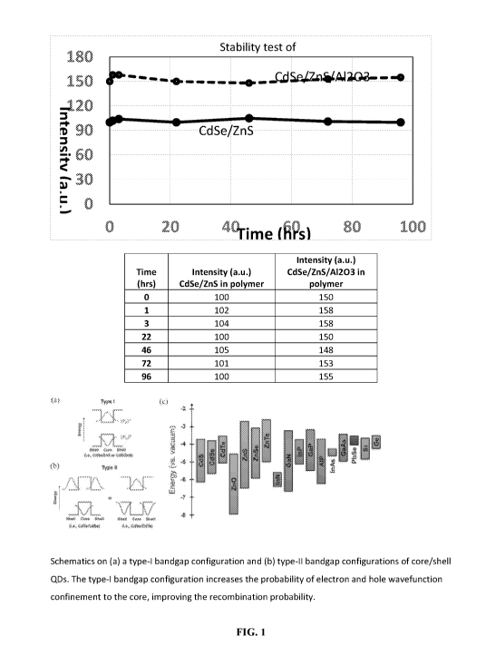
[0077] FIG. 1 is a schematic showing a type-I bandgap configuration and type-
II bandgap
configurations of core/shell QDs.
[0078] FIG. 2 is a schematic showing valence and conduction bands of am- and 7-
A1203 films grown by atomic layer deposition.
[0079] FIG. 3 is graph comparing intensity over time of CdSe/ZnS vs.
CdSe/ZnS/A1203
quantum dots demonstrating the stability imparted by the Al2O3 passivation
layer.
[0080] FIG. 4 depicts the surface of Al2O3 is characterized by a repeating
pattern of
electropositive and electronegative regions.
[0081] FIG. 5 is another depiction of the repeating pattern of electropositive
and
electronegative regions of the A1203 surface.
[0082] FIG. 6 is graph comparing intensity over time of polymer encapsulated
quantum dots
in accordance with some embodiments, showing stability of the polymer
encapsulated
quantum dots over time.
[0083] FIG. 7 depicts a multilayer film that includes a film containing
quantum dot cores in
accordance with some embodiments.
[0084] FIG. 8 depicts the effect of varied refractive indexes as employed by
different
embodiments disclosed herein.
9
CA 03024847 2018-11-19
WO 2017/201465
PCT/US2017/033630
100851 FIG. 9 depicts a multilayer film that includes multiple layers,
including a film
containing quantum dot cores in accordance with some embodiments.
[0086] FIG. 10 is a chart showing the emission spectrum for exemplary Cd-Free
quantum
dots in accordance with some embodiments.
[0087] FIG. 11 is a graph comparing stability testing of examples BI3 and B15
disclosed
herein.
[0088] FIG. 12 is a calibration curve developed from the data associated with
examples B1
through B6 disclosed herein.
[0089] FIG. 13 is a calibration curve developed from the data associated with
examples B7
through B11 disclosed herein.
[0090] FIG. 14 is an emission spectra of the solvent cast film of example B22
made using
excitation at 450 nm and the emission in the red wavelengths of the spectra.
[0091] FIG. 15 is an emission spectra of the melt extruded film of example B23
made using
excitation at 450 tun and the emission in the red wavelengths of the spectra.
DETAILED DESCRIPTION
[0092] Applicants have now discovered that by tightly bonding a polymer to the
outer
surface of the quantum dot, stability of the quantum dot can be maintained
even in a variety
of harsh manufacturing conditions, such as, but not limited to, extrusion
molding, injection
molding, and other techniques.
[0093] As described further below, in particular embodiments, the polymer is
chosen such
that it cross-links with the passivation layer (e.g. A1203) of the quantum dot
such that the
bond dissociation energy associated with the polymer/passivation layer is
greater than the
energy needed to melt the cross-linked polymer. In other words, the bond
between the
polymer and the passivation layer is not broken at extrusion (or other
manufacturing)
temperatures. This tight bond essentially protects the quantum dot during
melting operations
such as extrusion and injection molding. Previously, quantum dots exposed to
such
temperatures simply went dark, their optoelectronic properties extinguished by
the processing
conditions.
[0094] Described herein are methods for making quantum dots, quantum dot-
containing
polymer resins and the polymer resins themselves. These methods are applicable
to various
types of quantum dots provided the polymer can tightly bond to the surface of
the quantum
dot.
CA 03024847 2018-11-19
WO 2017/201465
PCT/US2017/033630
[0095] By tightly bonding a polymer to the outer surface of the quantum dot,
particularly a
passivated quantum dot, stability of the quantum dot can be maintained even in
a variety of
harsh manufacturing conditions, such as, but not limited to, extrusion
molding, injection
molding, cast molding, solvent casting, and other techniques.
[0096] As described further below, in particular embodiments, the polymer is
chosen such
that it cross-links with the passivation layer (e.g. A1203) of the quantum dot
such that the
bond dissociation energy associated with the bonds between the polymer and the
passivation
layer is greater than the energy needed to melt the cross-linked polymer. In
other words, the
bond between the polymer and the passivation layer is not broken at melt
temperatures
incurred, for example during extrusion (or other manufacturing) processes.
This tight bond
essentially protects the quantum dot during melting operations such as
extrusion and injection
molding. Previously, quantum dots exposed to such temperatures simply went
dark, their
optoelectronic properties were extinguished by the processing conditions.
[0097] Described herein are methods for making quantum dot-containing polymer
resins and
the polymer resins themselves. These methods are applicable to various types
of quantum
dots provided the polymer can tightly bond to the surface of the quantum dot.
100981 As noted above, although improved stability can be had by using the
polymers and
methods disclosed herein with any quantum dot, be it homogenous or alloy-
gradient, size-
tuned or stoichiometrically tuned, capped or uncapped, passivated or
unpassivated, so long as
the polymer can tightly bind to the outer surface of the quantum dotõ
achieving efficient and
stable quantum dot (QD) photoluminescense, over the visible range of light,
under the
combined conditions of high photon flux and chemically adverse external
environments
benefits from a multi-tiered approach.
[0099] First, the QD cores should have a similar surface area across the
visible range.
Additionally, it is specifically contemplated that cadmium-free (Cd-free)
quantum dots may
also be used in the methods and polymers described herein. Any Cd-free quantum
dot may
be used, but those described in US Provisional Patent Application No.
62/338,915 entitled
Cadmium-Free Quantum Dots, the disclosure of which is incorporated by
reference, and set
forth below, are well-suited for use with the methods and polymers disclosed
herein.
101001 Second, core passivation should provide both confinement of the exciton
wavefimction to the core and a physical barrier to water and oxygen.
[0101] Third, the dispersive matrix that provides separation in space for the
individual QDs
must also provide a stable electronic configuration outside the QD volume that
is conducive
to photoluminescense, while itself being stable against photodegradation. The
embodiment of
11
CA 03024847 2018-11-19
WO 2017/201465
PCT/US2017/033630
these three elements into usable materials for the thermoplastic, thermoset
and solvent cast
production of optical components would accelerate the acceptance of quantum
dot based
components for display and lighting applications.
101021 1. The Core
101031 It is a basic property of metal and semiconductor materials that their
propensity for
chemical reactions increases with an increase in surface area to mass. Thus, a
1 cm cube of
metal will simply heat up when exposed to flame while that same mass will
ignite if ground
to a micron-sized powder. The same is true of QD cores with respect to
environmental
degradation and photodegradation. QDs tuned by core size will differentially
degrade due to
the increased reactivity of smaller cores (blue-green emitters) versus larger
cores (yellow-red
emitters) because of a higher surface area to mass ratio. This is true in both
situations of
environmental attack by water and oxygen and under conditions of high photon
flux where
destructive free radicals are created on the QD surface. At the surface of
QDs, there is a
population of atoms that are incompletely part of the periodic 3D crystal
lattice of the
interior. These atoms have vacant or lone-pair electron orbitals. These
dangling bonds are the
source of undesired chemical reactions both with the external environment and
in non-
radiative carrier relaxation processes during the photoluminescent emission
cycle in which
electrons pool at these sites instead of recombining with a hole. This effect
is magnified with
smaller QDs that have a higher surface area/mass ratio than larger QDs.
101041 Thus, in an optical device composed of multi-colored size-tuned QDs, it
is likely that
faster degradation of the QDs emitting at the blue end of the visible spectrum
will be
observed overtime, especially under conditions of exposure to water and oxygen
combined
with high photon flux. It is desirable to have all QD cores in an
optoelectronic device be of
similar size.
101051 This desired core configurations can be achieved by using QDs
synthesized by the
methods of Nie (US 7981667 and US 84201550 and Qu (us 8454927). These QDs are
tuned
by composition and not by size.
101061 While same color size-tunable dots could be used, when considering the
entire visible
range, stoichiometrically-tuned quantum dots advantageously have the same size
regardless
of emission wavelength. Stoichiometrically-tuned quantum dots can be made in
accordance
with the Nie and Qu patents discussed above or other available methods. An
improved
method, involving the use of a pH controller to fine tune the emission
wavelength is disclosed
in US Provisional Patent Application No. 62/338,888 entitled Tunable
Semiconductor
12
CA 03024847 2018-11-19
WO 2017/201465
PCT/US2017/033630
Nanocrystals And Films And 3-D Structures Containing Them the disclosure of
which is
incorporated by reference and set forth below herein. Quantum dots made by the
methods
disclosed therein result in core/shell quantum dots having substantially the
same size
regardless of emission wavelength.
101071 CanpinE (i.e. first nassivation laver)
[0108] There are two methods to passivate the dangling bonds on the surface of
QDs for
higher quantum efficiency (QE) and improved photo/chemical stability: 1)
passivating with
low MW organic ligands or 2) passivating with inorganic shells. Passivation
with organic
ligands is simple and straightforward but the surface metal-organic ligand
bond is relatively
unstable and can be broken and displaced by chemical and/or photochemical
reactions.
Passivation with inorganic shells is embodied by the well-known core-shell
type of QD, and
is often referred to as "capping" such as with a ZnS shell. The surface
passivation of QD
cores with inorganic shells is more stable and has the additional desired
effect of providing
better confinement of the exciton waveftmction to the core, thus increasing
QE. If a QD core
is located within a shell material with a larger bandgap energy, the electron
and hole
wavefunctions are better confined to the core. The recombination probability
of the two
wavefunctions (electron and hole) increases while the non-radiative decay
process via
interaction with dangling bonds on the surface decreases. Bandgap and
electronic energy
levels for common group II-VI, III-V and II-VI semiconductors are shown in
Fig. 1.
[0109] These core-shell structures are improved with respect to QE and
photostability (PS)
but are still susceptible to chemical attack by water and oxygen from the
environment.
[0110] This capping is present in traditional core-shell quantum dots, and can
be applied to a
number of quantum dots, including the Cd-Free quantum dots and the
stoichimetrically/pH
controller tuned quantum dots disclosed herein, as well as other quantum dots.
[0111] 2. Passivation (second laver):
[0112] It is desirable to provide a second shell of an even wider bandgap
material over the
first shell that would further confine the exciton wavefunction, passivate the
dangling bonds
on the outer surface of the first shell material and provide a physical
barrier to the diffusion
of water and oxygen.
[0113] This can be realized by adding a second shell, a passivation layer, of
A1203 as
described in U.S. Patent No. 9,425,253 (Qu and Miller) hereby incorporated by
reference.
13
CA 03024847 2018-11-19
WO 2017/201465
PCT/US2017/033630
The bandgap of Al2O3 is between -3.5 and -11 (Fig. 2) which encompasses the
commonly
used II-VI and III-V QD core and shell materials.
[0114] In addition to having a bandgap energy that encompasses the commonly
used QD
core-shell materials. A1203, at a thickness of 4-5 atomic layers, has the
additional property of
providing an absolute or near-absolute barrier to the diffusion of oxygen and
water. This
provides a high barrier of protection from chemical attack by water and oxygen
on the
sensitive core-shell semiconductor materials.
101151 FIG. 3 shows the improved stability achieved by coating a traditional
CdSe/ZnS core-
shell quantum dot with an Al2O3 passivation layer.
[0116] 3. The dispersive matrix (i.e. the polymer)
[0117] The A1203surface layer offers unique synergistic opportunities to
provide a matrix
for QD dispersion that is chemically stable and electronically stable at the
QD/matrix
interface. The surface of A1203 is characterized by a repeating pattern of
electropositive and
electronegative regions as seen in Figs. 4 and 5.
[0118] QDs with an A1203 surface show very tight binding affinities to organic
ligands
containing ¨COOH and ¨SH groups and also polymers with repeating carbonyl
groups, such
as polymers described in invention disclosures by Nulwala assigned to
Crystalplex (U.S.
Patent Applciation Serial Nos. 62/338,888 and 62/338,915 both filed on May 19,
2016 and
incorporated herein by reference) and 14/725,658, which is hereby incorporated
by reference.
This tight bonding has multiple desirable effects in the resulting
QD/ligand/polymer matrix.
[0119] 3.1 Stability of the electronic configuration immediately outside of
the OD
volume
[0120] It is known that the electronic configuration of the volume immediately
adjacent to
the QD surface and extending out to the Exciton Bohr Radius can affect the
overall QE of a
QD population. (see, X. ji, D. Copenhaver, C. Sichmeller, and X. Peng, "Ligand
bonding
and dynamics on colloidal nanocrystals at room temperature: the case of
alkylamines on
CdSe nanocrystals," J. Am. Chem. Soc. 130(17), 5726-5735 (2008). S. F.
Wuister, C. de
Mello Donega, and A. Meijerink, "Influence of Thiol Capping on the Exciton
Luminescence
and Decay Kinetics of CdTe and CdSe Quantum Dots," J. Phys. Chem. B 108(45),
17393-
17397 (2004)) This is commonly seen when exchanging small MW organic ligands
on the
surface of a QD. Even though the QD nanocrystal is not physically changed by
the process, a
change in photoluminescent QE is observed. What is desired is a local
electronic
configuration that results in high QE for the QD and a very stable interface
between the QD
14
CA 03024847 2018-11-19
WO 2017/201465
PCT/US2017/033630
surface and the external matrix that remains unchanged even under extremes of
temperature,
high photon flux and destructive chemical environments. This can be achieved
by binding the
A1203 surface of the QD to polymers such as those disclosed by Nulwala. The
overall
binding energy of the matrix polymer to the A1203 surface can exceed the
energy of a 280 C
extrusion process and provide a stable QD/matrix interface.
[0121] 3.2 Chemical stability of the 00/matrix interface
[0122] In addition to heat, the stability of the QD/matrix interface also can
be compromised
by the presence of oxygen free radicals. These destructive free radicals can
be produced at the
QD/matrix interface by a combination of high photon flux and the presence of
02 molecules.
The destructive radicals can result in the breaking of covalent bonds in the
polymer chains in
the matrix (chain scission) and/or disruption of the multiple ionic bonds
between the matrix
polymer chains and the A1203 surface of the QDs.
[0123] The QD/matrix interface can be made resistant to oxygen free radical
attack by a
combination of the redundancy of ionic bonds between matrix polymers and the
A1203 surface and the intrinsic high 02 barrier properties of the matrix
polymer. Specific
polymers, notably homopolymers of cyclohexyl acrylate and cyclohexyl acrylate
copolymers
with methyl methacrylate or heptyl acrylate have repeating carbonyl units
oriented in 3D
space such that the electronegative carbonyl oxygen repeat distance matches
with the repeat
distance of the electropositive regions on the surface of A1203. This leads to
very tight
bonding of the polymer to the A1203 surface due to a multitude of binding
sites per polymer
chain.
101241 In addition, these acrylic polymers have high 02 barrier properties.
The combined
effect of suspending QDs in these matrices is very stable bonding of the
polymers to the QD
surface and minimal 02 diffusion to the binding site.
[0125] 3.3 Stable dispersion in the 3D matrix volume
[0126] In addition to the chemical stability of the QD/matrix interface, the
QDs must be well
dispersed without clumping to function properly in photoluminescent mode.
[0127] The polymers described in 3.2, and others disclosed by Nulwala,
disperse QDs in this
fashion. This is due to the fact that the polymer-QD bonding is more stable
than QD-QD self
bonding. Once bound in this fashion the QD/matrix is stable throughout
downstream
processing such as thermoplastic, thermoset and solvent-casting operations. In
addition, the
physical properties of the polymer matrix can be improved by the interaction
with the QD
nanoparticles. The physical crosslinking sites provided by the QDs can change
and improve
CA 03024847 2018-11-19
WO 2017/201465
PCT/US2017/033630
the physical properties of the polymer such as glass transition temperature,
durometer, impact
resistance, tensile strength and chemical resistance.
[0128] 4. Processing
[0129] 4.1 Preparation of the composite
[0130] The QD/polymer composite can be prepared by multiple methods.
[0131] Polymers can be polymerized in a continuous reactor and QDs can be
introduced into
the continuous stream either before or after complete polymerization. The
resulting
QD/polymer composite stream can then be collected and the solvent removed for
use as a
thermoplastic material to produce an optical component. Solvent may be
retained or added to
produce a solvent casting composite to produce an optical film.
[0132] Polymers can be completely polymerized then mixed with QDs in an
appropriate
solvent. Mixing, such as high shear mixing, can be applied to increase binding
of polymers
to the QD surface. The QD/polymer composite can be left as is for use in
solvent film casting
or the solvent can be removed to produce a dry composite for thermoplastic
processing to
produce optical components.
[0133] QDs can be suspended in monomer or a mixture of monomers or a mixture
of
monomers and oligomers or a mixture of monomers and multifunctional monomers
with
multiple vinyl groups that produce crosslinking in the final polymer. This
thermoset material
can later be cured by heat or UV radiation to produce the final optical
component.
[0134] 4.1 Downstream processing of the composite
[0135] The three commonly used processes to produce optical components from
plastics are
thermoplastic, thermoset, and solvent casting.
[0136] Included in these general categories are injection molding, extrusion,
thennoset
potting, thermoset film, solvent cast film, solvent cast ink jet printing,
solvent cast 3D
printing, thermoset ink jet printing, thermoset 3D printing, thermoplastic 3D
printing, and
other techniques.
[0137] Other than in the operating examples or where otherwise indicated, all
numbers or
expressions referring to quantities of ingredients, reaction conditions, etc.
used in the
specification and claims are to be understood as modified in all instances by
the term "about."
Accordingly, unless indicated to the contrary, the numerical parameters set
forth in the
following specification and attached claims are approximations that can vary
depending upon
the desired properties, which the present invention desires to obtain. At the
very least, and
16
CA 03024847 2018-11-19
WO 2017/201465
PCT/US2017/033630
not as an attempt to limit the application of the doctrine of equivalents to
the scope of the
claims, each numerical parameter should at least be construed in light of the
number of
reported significant digits and by applying ordinary rounding techniques.
[0138] Notwithstanding that the numerical ranges and parameters setting forth
the broad
scope of the invention are approximations, the numerical values set forth in
the specific
examples are reported as precisely as possible. Any numerical values, however,
inherently
contain certain errors necessarily resulting from the standard deviation found
in their
respective testing measurements.
[0139] Also, it should be understood that any numerical range recited herein
is intended to
include all sub-ranges subsumed therein. For example, a range of "1 to 10" is
intended to
include all sub-ranges between and including the recited minimum value of 1
and the recited
maximum value of 10; that is, having a minimum value equal to or greater than
1 and a
maximum value of equal to or less than 10. Because the disclosed numerical
ranges are
continuous, they include every value between the minimum and maximum values.
Unless
expressly indicated otherwise, the various numerical ranges specified in this
application are
approximations.
[0140] As used herein, the singular forms "a", "an" and "the" include plural
reference unless
the context clearly dictates otherwise.
[0141] As used herein, the term "about" means plus or minus 10% of the
numerical value of
the number with which it is being used. Therefore, about 50% means in the
range of 45%-
55%.
101421 As used herein, the term "copolymer" means a polymer resulting from the
polymerization of two or more polymerizable unsaturated molecules and is meant
to include
terpolymers, tetra polymers, etc.
[0143] As used herein, the term "core/shell" means particles that have a
quantum dot as a
core and one or more shells or coatings generally uniformly surrounding the
quantum dot
core. Non-limiting examples of shell materials include Cd or Zn salts of S or
Sc and/or metal
oxides.
101441 The terms "include," "comprise," and "have" and their conjugates, as
used herein,
mean "include but not necessarily limited to."
[0145] As used herein, the term "Group II element" is meant to include one or
more elements
from the IUPAC group 2 of the periodic table selected from Cd, Zn and Hg,
except when
discussing Cd-free embodiments, in which case Group II element refers one or
more elements
from the IUPAC group 2 of the periodic table selected from Cu, Zn and Hg.
17
CA 03024847 2018-11-19
WO 2017/201465
PCT/US2017/033630
[0146] As used herein, the term "Group VI element" is meant to include one or
more
elements from the IUPAC group 16 of the periodic table selected from S. Se,
Te, Po, and 0.
[0147] As used herein, the terms "nanoparticles", "nanocrystals", and
"passivated
nanocrystals" refer to small structures in which the ordinary properties of
their constituent
materials are altered by their physical dimensions due to quantum-mechanical
effects, often
referred to as "quantum confinement." For the sake of clarity, the use of
these terms in this
disclosure refers to objects possessing quantum-confinement properties, which
are separated
from one another in all three dimensions; enabling incorporation into liquids,
vapors, or
solids.
[0148] "Optional" or "optionally" means that the subsequently described
structure, event, or
circumstance may or may not be present or occur, and that the description
includes instances
where the structure is present and where it is not or instances where the
event occurs and
instances where it does not.
[0149] As used herein, the term "polymer" is meant to encompass, without
limitation,
oligomers, homopolymers, copolymers and graft copolymers.
[0150] As used herein, the term "quantum dot" typically refers to a
nanocrystalline particle
made from a material that in the bulk is a semiconductor or insulating
material, which has a
tunable photophysical property in the near ultraviolet (UV) to far infrared
(IR) range, and in
particular, the visible range. In many embodiments of the present invention
the term
quantum dot includes semiconductor nanocrystals (SCN) that include transition
metals, non-
limiting examples being Cd and Zn, and anions from the IUPAC group 16 of the
periodic
table, non-limiting examples being Se, S, Te, and 0.
[0151] As used herein, the term "composite" refers to materials that contain
quantum dots
and a polymer combined into a matrix that includes quantum dots dispersed
throughout the
matrix. In some embodiments, the quantum dots are dispersed substantially
evenly
throughout the matrix.
[0152] Aspects of this disclosure relate to semiconductor nanocrystals tuned
to a
predetermined emission wavelength (i.e. a quantum dot). In some instances, the
quantum
dots may be a plurality of quantum dots containing a ranges of predetermined
emission
wavelengths. Particularly, in some embodiments, a plurality of quantum dots
contains a
homogenous mixture of quantum dots emitting a desired plurality of desired
wavelengths.
[0153] Aspects of the present invention relate to films and 3-D structures
comprising
core/shell quantum dot particles dispersed in a aciylate resin. The films and
3-D structures
provide the ability to cast films and place 3-D structures onto commercially
applicable
18
CA 03024847 2018-11-19
WO 2017/201465
PCT/US2017/033630
equipment resulting in highly stable quantum dot - polymer composite films and
3-D
structures. The inventive films and 3-D structures can be used in display and
lighting
applications. In particular aspects, a single-coat down-conversion film (SCDF)
that includes
a single layer of the quantum dot - polymer composite film, sandwiched between
at least two
transparent films and 3-D structures can be used. The single and multilayer
inventive films
and 3-D structures enable a simpler and more cost effective product that
provides at least the
performance of more complicated structures.
The Quantum Dot Core
101541 Any semiconductor nanoctystals known in the art may be used as the core
for the
quantum dots for incorporation into the polymers described herein, non-
limiting examples
being the relevant semiconductor nanocrystals disclosed in U.S. Patent Nos.
6,207,229;
6,322,901; 6,576,291; 6,821,337; 7,138,098; 7,825,405; 7,981,667; 8,071,359;
8,288,152;
8;288;153; 8;420,155; 8,454,927; 8,481,112; 8,481,113; 8,648,524; 9,063,363;
and 9;182;621
and U.S. Published Patent Application Nos. 2006/0036084, 2010/0270504,
2010/0283034;
2012/0039859; 2012/0241683; 2013/0335677; 2014/0131632; and 2014/0339497.
[0155] The quantum dots employed herein may be any quantum dot, and may be:
a) cadmium-containing or cadmium free
b) alloy-gradient or non-gradient (i.e. homogenous)
c) size-tunable, stoichiometrically-tunable, or not, or
d) any combination of these.
[0156] Additionally, contemplated herein are new methods of making quantum
dots,
particularly a method of making same-size stoichimetrically and pH controller-
tuned
quantum dots and Cd-free quantum dots are disclosed herein, in and of
themselves, and also
for incorporation into the polymers as disclosed herein.
[0157] Thus, traditional core/shell quantum dots such as those that are
commercially
available, other Cd-free quantum dots, as well as the same-size
stoichimetrically and pH
controller-tuned quantum dots and Cd-free quantum dots described and disclosed
herein may
be incorporated into the polymers as described further below.
[0158] Cd-Free Quantum Dots
101591 As used herein, the term "Cd-free" means the object so described is
substantially free
of cadmium or was made without using cadmium, or does not contain cadmium. For
example, the terms "Cd-free semiconductor nanocrystals" and Cd-free
semiconductor
19
CA 03024847 2018-11-19
WO 2017/201465
PCT/US2017/033630
quantum dots" refer to semiconductor nanocrystals or quantum dots that are
substantially free
of, made without using or do not contain cadmium.
[0160] "Substantially free of cadmium" means containing less than 5% cadmium,
less than
3% cadmium, less than 1%, less than 0.5%, less than 0.3%, less than 0.1% or
any range of
values between any two of these values and any value there between.
[0161] As used herein, with respect to Cd-Free quantum dots, the term "Group
II element" is
meant to include one or more elements from the TUPAC group 2 of the periodic
table selected
from Cu, Zn and Hg.
[0162] As used herein, the term "Group III element" is meant to include one or
more
elements selected from In, Ga, Al, and Ti.
[0163] As used herein, the term "Group VT element" is meant to include one or
more
elements from the IUPAC group 16 of the periodic table selected from S, Se,
Te, Po, and 0.
[0164] In some embodiments, suitable Cd-free semiconductor nanocrystals that
can provide
useful quantum dot cores include, but are not limited to, semiconductor
nanocrystals (SCN) of the formula ABCD where A is a Group II element, B is
another group
II element, C is a group III element, and D is a group VI element.
[0165] In particular embodiments the Group II element can be one or more
selected from Cu,
Zn and Hg, the group III element can be one or more selected from In, Ga, Al,
and the group
VI element can be can be one or more selected from S, Se, Te, Po, and 0.
[0166] In particular embodiments, the Cd-free nanoparticles are ZnCuInS and/or
ZnCuGaS
[0167] In other particular embodiments, suitable semiconductor nanocrystals
that can provide
useful Cd-free quantum dot cores in the invention include semiconductor
nanocrystals (SCN) of the formula ABCDE where A is a first Group II element, B
is second
group II element, C is a first group III element, D is a second III group
element, and E is a
group VI element.
[0168] In further aspects of this particular embodiment the Group II element
can be one or
more selected from Cu, Zn and Hg, the group III element can be selected from
In, Ga, Al, and
the group Vi element can be selected from S, Se, Te, Po, and 0.
[0169] In additional specific aspects of this particular embodiment, the Cd-
free nanoparticles
are ZnCuInAlS and/or ZnCuInGaS.
[0170] In further embodiments, suitable Cd-free semiconductor nanocrystals
that can provide
quantum dot cores useful in the invention include semiconductor
nanocrystals
(SCN) of the formula ABCDE where A is a first Group II element, B is second
group II
CA 03024847 2018-11-19
WO 2017/201465
PCT/US2017/033630
element, C is a group III element, D is a first group VI element, and E is a
second group
element.
[0171] In aspects of this further embodiment the Group II element can be one
or more
selected from Cu, Zn and Hg, the group III element In, Ga, Al, and the group
Vi element can
be selected from S, Se, Te, Po, and 0.
[0172] In a specific aspect of this further embodiment, the Cd-free
nanoparticles are
ZnCuInSSe, ZnCuGaSSe, ZnCuAlSSe and combinations thereof.
[0173] In additional embodiments, suitable Cd-free semiconductor nanoctystals
that can
provide quantum dot cores useful in the invention include 11-II-III-111-V1-VI
semiconductor
nanocrystals (SCN) of the formula ABCDEF, where A is a first Group II element,
B is a
second group IT element, C is a first group ITT element, D is a second group
ITT element, and D
is a group element, E is a first group VI element, and F is a second group VI
element.
[0174] In aspects of this additional embodiment the Group II elements can be
one or more
selected from Cu, Zn and Hg, the group TIT elements can be one or more
selected from In, Ga,
Al, and the group Vi elements can be one or more selected from S, Se, Te, Po,
and 0.
[0175] In specific aspects of this additional embodiment, the Cd-free
nanoparticles can be
ZnCuInAlSSe, ZnCuInGaSSe, ZnCuAlGaSSe and combinations thereof.
[0176] Source of Group II and Group III elements
[0177] In some embodiments, the source of the group II and group III elements
are metal
oxides.
[0178] In particular embodiments, source of the group II and group III
elements can be
selected from ZnO, CuO, In203, A1203.
[0179] In some embodiments, the source of the group 11 and 111 elements are
fatty acid salts.
[0180] In particular embodiments, the group II and group III elements can be
selected from
ZnX, CuX, InX, AIX. X can be a carboxylic acid with chain length from Cl to
C22.
[0181] Any suitable carboxylic acid can be used. In some embodiments, the
carboxylic acids
used can be one or more selected from acetic acid, propionic acid, butyric
acid, myristoleic
acid, palmitoleic acid, sapienic acid, oleic acid, elaidic acid, vaccenic
acid. linoleic acid,
linoelaidic acid, a-Linolenic acid, arachidonic acid, eicosapentaenoic acid,
erucic acid,
docosahexaenoic acid, stearic acid, palmitic acid, and arachidic acid.
[0182] In a particular embodiment, the carboxylic acid is oleic acid.
[0183] In a specific embodiment, the carboxylic acid is acetic acid.
[0184] Source of VI elements
21
CA 03024847 2018-11-19
WO 2017/201465
PCT/U52017/033630
[0185] In some embodiments, the source of the group VI elements is a pure
elemental
powder.
[0186] In particular embodiments, the group VI elements can be selected from
elemental S.
Se, Te, Po, and 0.
[0187] In some embodiments, the source of the group VI elements are group VI
element
containing molecules.
[0188] In particular embodiments, the group VT element is present as the
corresponding
thiolate of a single functional alkyl thiol containing molecule, such as but
not limited to, alkyl
thiols with a chain length of from Cl to C22.
[0189] In specific embodiments, the group VI element is the thiolate of 1-
Dodecanthiol.
[0190] In particular embodiments, the group VI element can be a dithiolate of
the
corresponding dithiol molecules, such as but not limited to those dithiol
molecules having a
chain length of from Cl to C22.
[0191] Ligands
[0192] In embodiments, the Cd-free nanoparticles are coated with ligands.
101931 In particular embodiments, the ligands can be selected from single
chain fatty acids
with chain lengths from C8 to C22.
[0194] Any suitable fatty acid can be used. In some embodiments, the fatty
acids used can be
one or more selected from myristoleic acid, palmitoleic acid, sapienic acid,
oleic acid, elaidic
acid, vaccenic acid, linoleic acid, linoelaidic acid, a-Linolenic acid,
arachidonic acid,
eicosapentaenoic acid, erucic acid, docosahexaenoic acid, stearic acid,
palmitic acid, caprylic
acid and arachidic acid.
[0195] In specific embodiments, the fatty acid ligands include caprylic or
octanoic acid.
[0196] In particular embodiments, the ligands can be selected from single
chain thiols with
chain lengths from Cl to C22.
[0197] In specific embodiments, the ligands include 1-Dodecanthiol.
[0198] In particular embodiments, the ligands can be a mixture of fatty acid
and long chain
thiols with a chain length of from CI to C22.
[0199] In specific embodiments, the ligands are a mixture of 1-Dodecanthiol
and Octanoic
acid.
[0200] Solvent
[0201] In some embodiments, the solvents used for the synthesis of Cd-free
nanoparticles
include one or more C12 to C20 hydrocarbons. In many embodiments, the
precursor solution
solvents can be chosen as required by the physical properties of the materials
used in the
22
CA 09024847 2018-11-19
WO 2017/201465
PCT/1JS2017/033630
precursor solution and as required by the apparatus available for synthesis.
In particular
embodiments, a high boiling organic solvent is employed, typically with a
boiling point
above about 150, in some cases above about 200, and in other cases above about
225 C.
[0202] In particular embodiments, the solvent includes one or more selected
from
octadecane, dodecane, hexadecane and icosane.
[0203] In some embodiments, tributylphosphine (TBP) is used as a solvent in
the precursor
solution. In other embodiments, a mixture of 'TBP and C12 to C20 hydrocarbons
are used in
the precursor solution. In these embodiments, including TBP can be
advantageous because it
provides a strong dipole moment, which can aid in dissolving the Group VI
elements. In
many embodiments, the precursor solution solvents can be chosen as required by
the physical
properties of the materials used in the precursor solution and as required by
the apparatus
available for synthesis.
[0204] Cd-free Core Syntheses
[0205] Some embodiments provide a method for synthesizing Cd-free
semiconductor
nanocrystal cores. The method includes heating a precursor solution that
includes the desired
mixture of Group II element(s), Group III elements(s) and Group VI element(s)
as described
above in one or more solvents that include one or more C12 to C20 hydrocarbons
and one or
more fatty acids to a temperature sufficient to produce the Cd-free
semiconductor nanociystal
cores.
[0206] In some embodiments, the emission wavelength of the synthesized Cd-free
nanoparticles is detemiined by molar ratio of the precursors, and the
concentration in and
type of C12 to C20 hydrocarbon solvent. Once the proper amounts of chemicals
needed for
the syntheses are weighed, they are placed in a suitable reaction vessel.
Without degassing
the temperature is raised sufficiently to initiate the reaction, and keep at
that temperature for a
period of time sufficient to allow the reaction to equilibrate.
[0207] In some embodiments, the reaction temperature is at least about 200 C,
in some cases
at least about 220 C, in other cases at least about 240 C and in some
instances at least about
250 C and can be up to about 300 C, in some cases up to about 280 C and in
other cases up
to about 270 C. The temperature employed will depend on the particular
precursors and
solvents used. The reaction temperature can be any value or range between any
of the values
recited above.
[0208] In some embodiments, the reaction time is at least about 5 minutes, in
some cases at
least about 8 minutes and in other cases at least about 9 minutes and can be
up to about 60
minutes, in some cases up to about 45 minutes, in other cases up to about 30
minutes and in
23
CA 03024847 2018-11-19
WO 2017/201465
PCT/US2017/033630
some instances up to about 15 minutes. The reaction time employed will depend
on the
particular precursors and solvents used. The reaction time can be any value or
range between
any of the values recited above.
[0209] In a specific embodiment, the reaction time is about 10 minutes.
[0210] Core Purification
[0211] Purification of the Cd-free nanoparticle cores is performed to
substantially reduce or
eliminate unreacted precursors and byproducts generated during the reaction.
In some
embodiments, purification of the Cd-free nanoparticle cores can be
accomplished by:
102121 1) Transferring the Cd-free nanoparticle core synthesis solution to a
centrifuge tube
and diluting to 7.5 times its volume with a 1:3 mixture of a nopolar and polar
solvent (a non-
limiting example being hexanes and butanol).
[0213] 2) Centrifuging the solution from (1) until crystal pellets form, and
pouring off the
supernatant.
[0214] 3) Washing the crystals three times with a 1:3 mixture of a nonpolar
and polar solvent
(a non-limiting example being hexane and methanol), using 6.5 times the volume
of the
original Cd-free nanoparticle core synthesis solution for each wash. First
adding the nonpolar
solvent to suspend the crystals and then adding the polar solvent to
precipitate them.
[0215] 4) Suspending the crystals in a nonpolar solvent (a non-limiting
example being
hexane) at 81% the volume of the synthesis solution.
[0216] Non-traditional QDs: Stoichiometrically/pH controlled tuning
[0217] The embodiments below relate to a quantum dot made in accordance with
the
teachings of U.S. Provisional Patent Application No. 62/338,888, employing a
pH controller
in methods for stoichiometrically tuning QDs to aid in establishing the
desired emission
wavelength.
[0218] In some embodiments, the core is a II-VI-VI semiconductor nanocrystal
(SCN)
having a predetermined emission wavelength. In some embodiments, these are
made by
heating a II-VI-VI SCN precursor solution that includes a Group II element, a
first Group VI
element, a second Group VI element, and a pH controller in one or more
solvents that
together include one or more C12 to C20 hydrocarbons and one or more fatty
acids to a
temperature sufficient to produce the 11-VI-VI SCNs. The amount of pH
controller is
adjusted to provide the predetermined emission wavelength from the SCNs.
24
CA 03024847 2018-11-19
WO 2017/201465
PCT/US2017/033630
[0219] Without wishing to be bound by theory, Applicants believe that the use
of oleic acid
creates superior quantum dots because they are well-suited for subsequent
capping,
particularly with ZnS.
[0220] Pre-Cursor Solution
[0221] In some embodiments, suitable semiconductor nanocrystals that can
provide quantum
dot cores useful in the present invention include 11-V1-V1 semiconductor
nanocrystals (SCN)
of the formula WYNZ(1-x) where W is a Group II element, Y and Z are different
Group VT
elements, and 0<X<1.
[0222] In particular embodiments the Group 11 element can be one or more
selected from Cd,
Zn and Hg and the Group VI element can be one or more selected from S. Sc, Te,
Po, and 0.
[0223] In some embodiments, the source of the group VI elements is soluble in
C12 to C20
hydrocarbons and are organic miscible with the one or more fatty acids used to
make the II-
VI-VI II-VI-VI SCN. In many embodiments, pure group VI elements in powder form
are
used.
[0224] In particular embodiments, a desired predetermined emission wavelength
to be
emitted from the SCNs is identified and the amount of pH controller is
adjusted such that the
resultant SCNs have the predetermined emission wavelength.
[0225] pH Controller
[0226] In some embodiments, the amount of pH controller is selected to tune
the emission
maximum wavelength of the SCN to the desired predetermined emission
wavelength. When
a specific wavelength is desired, a few synthesis reactions using different
concentrations of
pH controllers and, optionally, different molar ratios of precursors are run
to construct a
calibration curve. The required concentration of pH adjuster and, if
determined, the required
ratio of precursors are then identified for the desired wavelength from the
calibration curve.
[0227] In particular aspects of this embodiment, the emission wavelength from
the SCNs,
without pH controller, can be any wavelength in the visible range, and in
particular from
about 400 nm to about 700 nm, and any wavelength between those values. That
is, SCNs can
be made with a known emission wavelength. Then by introduction of a pH
controller that
emission wavelength can be "tuned" from that known emission wavelength to a
desired
predetermined wavelength.
[0228] When the pH controller is included in the precursor solution, the
emission wavelength
of the SCN shifts to a longer wavelength. In some aspects, the SCN emission
wavelength can
increase at least 3 nm, in some cases at least 5 nm and in other cases at
least 7 nm and can
increase up to 25nm, in some cases up to 20nm, and in other cases up to 17 nm
for each 0.1
CA 03024847 2018-11-19
WO 2017/201465
PCT/US2017/033630
weight percent of pH controller included in the precursor solution. The amount
of SCN
emission wavelength can be any value or range between any of the values
recited above. The
amount of SCN emission wavelength increase can vary based on the size of the
semiconductor nanocrystals, the particular pH controller used and the
particular Group II and
Group VI elements used. Through manipulation of these factors, the emission
wavelength
can be precisely tuned to a desired emission wavelength.
[0229] The pH controller is included in the precursor solution at a level that
provides the
desired SCN emission wavelength increase, often referred to as "tuning" the
SCN. The pH
controller can be present in the precursor solution at a level of from about
0.01 weight
percent of the precursor solution, in some cases about 0.1 weight percent of
the precursor
solution, in other cases about 0.15 weight percent of the precursor solution
and in some
instances about 0.2 weight percent of the precursor solution and can be up to
about 1 weight
percent of the precursor solution, in some cases up to about 0.9 weight
percent of the
precursor solution, in other cases up to about 0.8 weight percent of the
precursor solution and
in some instances up to about 0.7 weight percent of the precursor solution.
The amount of
pH controller will be an amount sufficient to achieve the desired tuning and
will typically not
exceed an amount that will increase the SCN emission wavelength beyond the
visible
spectrum. The amount of pH controller in the precursor solution can be any
value or range
between any of the values recited above.
[0230]
[0231] Any pH controller that can maintain a desired pH and effect the
emission wavelength
tuning described above can be used in the SCN solution. In some embodiments,
the pH
controller can be an oxide or carboxylic acid salt of a Group II element. In
particular
embodiments the pH controller can be selected from zinc salts of acetic acid,
citric acid,
lactic acid, propionic acid, butyric acid, tartaric acid, and valeric acid. In
particular
embodiments, the pH controller is an oxide or carboxylic acid salt of a Group
II element.
[0232] In some aspects of the invention, the pH controller is selected from
zinc salts of acetic
acid, citric acid, lactic acid, propionic acid, butyric acid, tartaric acid,
and valeric acid.
[0233] In some embodiments, the C12 to C20 hydrocarbons used in the SCN
solution can be
one or more selected from hexadecene, octadecene, eicosene, hexadecane,
octadecane and
Tcosane.
[0234] In other embodiments, the fatty acids used in the SCN solution can be
one or more
selected from myristoleic acid, palmitoleic acid, sapienic acid, oleic acid,
elaidic acid,
vaccenic acid, linoleic acid, linoelaidic acid, a-Linolenic acid, arachidonic
acid,
26
CA 03024847 2018-11-19
WO 2017/201465
PCT/US2017/033630
eicosapentaenoic acid, erucic acid, docosahexaenoic acid, stearic acid,
palmitic acid, and
arachidic acid.
[0235] Any pH controller that can maintain a desired pH and effect the
emission wavelength
tuning described above can be used in the precursor solution. In some
embodiments, the pH
controller can be an oxide or carboxylic acid salt of a Group II element. In
particular
embodiments the pH controller can be a salt of an acid selected from the group
consisting of
acetic acid, citric acid, lactic acid, propionic acid, butyric acid, tartaric
acid, and valeric acid.
In some embodiments, the salt is a zinc salt of an acid selected from the
group consisting of
acetic acid, citric acid, lactic acid, propionic acid, butyric acid, tartaric
acid. and valeric acid.
[0236] In embodiments, the pH controller is soluble in the one or more fatty
acids used in the
precursor solution.
[0237] Hydrocarbon solvent
[0238] Any suitable C12 to C20 hydrocarbons can be used in the precursor
solution. In some
embodiments, the C12 to C20 hydrocarbons in the precursor solution can include
one or more
hydrocarbons selected from hexadecene, octadecene, eicosene, hexadecane,
octadecane and
icosane.
[0239] In some some embodiments, tributylphosphine (TBP) is used as a solvent
in the
precursor solution. In other embodiments, a mixture of TBP and C12 to C20
hydrocarbons
are used in the precursor solution. In these embodiments, including TBP can be
advantageous because it provides a strong dipole moment, which can aid in
dissolving the
Group VI elements. In many embodiments, the precursor solution solvents can be
chosen as
required by the physical properties of the materials used in the precursor
solution and as
required by the apparatus available for synthesis.
[0240] Fatty Acid
[0241] Any suitable fatty acid can be used in the precursor solution. In some
embodiments,
the fatty acids used in the precursor solution can be one or more fatty acids
selected from
myristoleic acid, palmitoleic acid, sapienic acid, oleic acid, elaidic acid,
vaccenic acid,
linoleic acid, linoelaidic acid, a-Linolenic acid, arachidonic acid,
eicosapentaenoic acid,
erucic acid, docosahexaenoic acid, stearic acid, palmitic acid, and arachidic
acid.
102421 in a particular embodiment of the invention, the fatty acid is oleic
acid.
[0243] In particular embodiments, the II-VI-VI SCN precursor is prepared by
dissolving the
Group II element, the first Group VI element, and the second Group VI element
in a solvent
that includes the pH controller, octadecene and a fatty acid to provide the 11-
V1-V1 SCN
precursor solution.
27
CA 03024847 2018-11-19
WO 2017/201465
PCT/US2017/033630
[0244] In other embodiments, the II-VI-VI SCN precursor is prepared by
preparing a first
solution by dissolving the Group 11 element and the first Group VI element in
a first solvent
that includes octadecene and a fatty acid; preparing a second solution by
dissolving the
second Group VI element in a second solvent that includes octadecene; mixing
the first and
second solutions to provide a II-VI-VI SCN precursor solution. In this
embodiment, both of
the first and second solutions include the pH controller.
[0245] In additional embodiments, the IT-VT-VT II-VI-VI SCN precursor is made
by
preparing a first solution by dissolving a Group II element in a first solvent
that includes
octadecene and a fatty acid; preparing a second solution by dissolving a first
Group VI and a
second Group VI element in a second solvent that includes octadecene; and
mixing the first
and second solutions to provide a II-VI-VI SCN precursor solution. In this
embodiment, both
of the first and second solutions include the pH controller.
[0246] In further embodiments, the II-VI-VI SCN precursor is prepared by
preparing a first
solution by dissolving a Group II element in a first solvent that includes
octadecene and a
fatty acid; preparing a second solution by dissolving a first Group VI element
in a second
solvent that includes octadecene; preparing a third solution by dissolving a
second Group VI
element in a third solvent that includes tributylphosphine; and mixing the
first, second, and
third solutions to provide a IT-VT-VI SCN precursor solution. In this
embodiment, one or
more of the first, second and third solutions include the pH controller.
[0247] In all of the embodiments described above, the II-VI-VI semiconductor
nanocrystals
are synthesized by heating the II-VI-VI SCN precursor solution to a
temperature sufficient to
form the desired quantum dot core. In embodiments, the precursor solution
temperature is at
least 2000, in some cases at least 225 , in many cases at least 250 and in
many instances at
least 270 C and can be up to about 400 , in some cases up to about 3500 and
in other cases
up to about and 330 C. The temperature at which the II-VI-VI semiconductor
nanocrystals
are grown will vary depending on the particular Group II and Group VI elements
and ratios
used as well as the solvents, fatty acids and pH controller employed.
[0248] In all of the embodiments described above, the TI-VI-VI semiconductor
nanocrystals
are synthesized by heating the II-VI-VI SCN precursor solution to a
temperature described
above for a period of time that is at least sufficient to fonn the desired
quantum dot core. In
some embodiments, the reaction time is at least 40, in some cases at least 50,
in many cases at
least 60 and in many instances at least 70 minutes and can be up to about 120,
in some cases
up to about 110 and in other cases up to about 100 minutes. The reaction time
over which the
II-VI-VI semiconductor nanocrystals are grown will vary depending on the
temperature, the
28
CA 03024847 2018-11-19
WO 2017/201465
PCT/US2017/033630
particular Group II and Group VI elements and ratios used as well as the
solvents, fatty acids
and pH controller employed.
[0249] In a particular embodiment of the invention, the quantum dot core can
be prepared by
selecting Group II elements that are soluble in the fatty acid. Non-limiting
examples of
suitable fatty acids being stearic acid and oleic acid. The pH controller
soluble in the fatty
acid, an oxide or acetate of a Group 11 element, is used. The source of the
Group VI elements
are chosen such that they are soluble in an organic solvent that is miscible
with the fatty acid
used to dissolve the Group II. In this embodiment, the organic solvent can be
tributylphosphine and/or octadecene.
[0250] In this embodiment, the pH, or electrical environment of the reaction
system is
determined by introducing the pH controller into the reaction system. The pH
controller is
selected based on having a negative or positive charge depending on the
desired type of
nanocrystal and the properties of precursors being used; and are miscible with
the reaction
system employed. In particular embodiments, the pH controller is Zinc acetate.
102511 Further to this embodiment, once the pH controller, solvents, and
elements are
selected, solutions of the elements are prepared in aliquots that are mixed
together for
nanocrystal synthesis. After mixing, the reaction is allowed to go to
completion.
[0252] In this embodiment, the emission maximum is determined by 1) the molar
ratio of the
two group six elements; and 2) the concentration of PH controller.
[0253] The present invention provides methods of tuning a quantum dot core.
The inventive,
convenient method for tuning the emission maximum wavelength of the resulting
quantum
dot cores includes identifying a desired emission maximum. Once a specific
wavelength is
identified, a few synthesis reactions varying the molar ratios of the
precursors and the
concentration of the pH controller can be performed to identify the molar
ratios of the
elements and concentration of pH controller that provide the desired
wavelength. In many
some embodiments, a calibration curve can be constructed by performing the
synthesis
reactions outlined above using different ratios of elements and concentrations
of pH
controller. Once the calibration curve is constructed, the ratios of elements
and concentration
of pH controller can be identified for any desired emission maximum.
[0254] Particular advantages to some of the embodiments of the present
invention include not
having to rely on a particular reaction time. Once the pH controller and stock
solutions are
prepared, aliquots of each can be mixed together and stirred at a temperature
sufficient to
support crystal growth, in many embodiments from about 200 C to about 400 C,
for about
40 to about 120 minutes. Advantageously, it is not important to end the
reaction at a specific
29
CA 03024847 2018-11-19
WO 2017/201465
PCT/US2017/033630
time. Once the method according to the invention is followed and the reaction
is complete
the solution can continue to be stirred at growth temperatures without
altering the final
quantum dot core product. In many prior art methods of synthesizing
nanocrystals, an
additional 1 to 5 seconds of extra reaction time substantially alters the
product.
[0255] In particular embodiments, the semiconductor materials of the quantum
dot cores may
have a gradient of one or more of the semiconductor materials radiating from
the center of the
nanocrystal or quantum dot to the outermost surface of the nanocrystal. Such
nanocrystals or
quantum dots are referred to herein as "concentration-gradient quantum dots."
For example,
in some embodiments, a concentration-gradient quantum dot having at least a
first
semiconductor and a second semiconductor may be prepared such that the
concentration of
the first semiconductor gradually increases from the center of the
concentration-gradient
quantum dot to the surface of the quantum dot. In such embodiments, the
concentration of the
second semiconductor can gradually decrease from the core of the concentration-
gradient
quantum dot to the surface of the quantum dot. Without wishing to be bound by
theory,
concentration-gradient quantum dot may have a band gap energy that is non-
linearly related
to the molar ratio of the at least two semiconductors.
[0256] Concentration-gradient quantum dots may be prepared from any
semiconductor
material known in the art including those semiconductor materials listed
above, and
concentration-gradient quantum dots may be composed of two or more
semiconductor
materials. In particular embodiments, concentration-gradient quantum dots may
be alloys of
CdSeTe having a molecular formula CdS1-xTex, CdSSe having a molecular formula
CdS1-
xSex, CdSTe having a molecular formula CdS1-x Tex, ZnSeTe having a molecular
formula
ZnSel-x Tex, ZnCdTe having a molecular formula Znl-x CdxTe, CdHgS having a
molecular
formula Cdl-x HgxS, HgCdTe having a molecular formula HgCdTe, InGaAs having a
molecular formula InGaS, GaAlAs having a molecular formula GaAlAs, or InGaN
having a
molecular formula InGaN, where x in each example can be any fraction between 0
and 1.
[0257] The methods described above provide various uncapped semiconductor
nanociystals,
referred to collectively as quantum dot cores herein.
[0258] Some embodiments provide quantum dot cores and in particular II-VI-VI
semiconductor nanocrystals made according to the methods described above.
[0259] Some embodiments provide quantum dot cores and IT-VT-VI semiconductor
nanocrystal that include Cd, S and Se, where the nanocrystal has been modified
by a zinc
alkylcarboxylate (such as zinc acetate). The quantum dot cores and II-VI-VI
semiconductor
nanocrystals generally correspond to the formula WYxZ(1-x) where W is a Group
T1 element,
CA 03024847 2018-11-19
WO 2017/201465
PCT/US2017/033630
Y and Z are different Group VI elements, and 0<X<1. In particular embodiments,
the
quantum dot cores and II-VI-VI semiconductor nanocrystals have a predetermined
emission
wavelength.
102601 The II-VI-VI semiconductor nanocrystals of the invention can have any
diameter,
and, thus, be of any size, provided that quantum confinement is achieved. In
certain
embodiments, the II-VI-VI semiconductor nanocrystals described herein have a
primary
particle size of less than about 10 nm in diameter. According to other
embodiments, the II-
VI-VI semiconductor nanocrystals have a primary particle size of between about
1 to about
500 nm in diameter. In other embodiments, a primary particle size of between
about 1 to
about 100 urn in diameter, and in still other embodiments, a primary particle
size of between
about 5 to about 15 nm in diameter. As used herein, the phrase "primary
particle" refers to the
smallest identifiable subdivision in a particulate system. Primary particles
can also be
subunits of aggregates.
102611 Standard core/shell Quantum dots (CdSe/ZnS)
[0262] Standard core/shell quantum dots of the CdSe/ZnS variety were obtained
from a
commercial source. The quantum dots were processed to assess the stability of
the quantum
dots with and without an A1203 passivation layer, and the stability of the
quantum dots with
and without the A1203 passivation layer additionally with an without
incorporation into the
polymer matrix described herein. FIG. 6 depicts the results of those tests.
[0263] To assess the effect of the A1203 passivation layer. QDs with and
without the A1203
passivation layer were coated naked on glass slides and exposed to 85/85
conditions (85 C,
85% humidity.) There was a marked difference as seen in FIG. 6 between Al2O3
pasisvated
QDs and those that without the Al2O3 passivation. The relative intensity is
not necessarily
important in this analysis, but the drop in the intensity of the QDs without
Al2O3 passivation
layer indicates a much less stable QD.
[0264] FIG. 6 shows that a core/shell QD with or without the A1203 passivation
layer
benefits from incorporation in the polymer as described below herein. Here,
QDs with and
without the passivation layer were dispersed and embedded in the polymer
described herein
and tested under the 85/85 test conditions. FIG. 6 shows that the dispersion
in the polymer
lead to stable QDs for both samples. Thus, dispersion within the polymer as
disclosed herein
leads to stable QDs.
31
CA 03024847 2018-11-19
WO 2017/201465
PCT/US2017/033630
[0265] Shell growth (capping) of Cd-Free nanoparticle cores
[0266] Capping the purified Cd-free nanoparticle cores can be accomplished by
the following
methods.
[0267] Method 1:
102681 Maintaining an oxygen free environment during the capping process. Take
a sample
of the purified Cd-free nanoparticle cores and perform the steps below. The
quantities
indicated are for every 0.1 mmol of Group IT element in the Cd-free
nanoparticle core
solution.
[0269] 1) Vacuum purging until the nonpolar solvent has evaporated.
[0270] 2) Adding 4.00 g trioctylphosphine oxide, and vacuum purging for 10
minutes.
Optionally, 0.2 g stearic acid can be added along with the trioctylphospine
oxide prior to
performing the vacuum purge, if a shell comprising stearic acid is desired.
[0271] 3) Heating to about 100 C for about 30 minutes under vacuum and then
to 200 C
without vacuum for 30 minutes.
[0272] 4) Preparing a capping solution by mixing 40 pL Zn(CH3)2, 80 pL
Hexamethyldisilathiane (CAS#3385-94-2), and 2.00 mL trioct3,71phosphine in an
oxygen-free
environment.
[0273] 5) Dripping the capping solution into solution (3) at about 200 ¨ 220
C over about 5
minutes for every 2.0 mL trioctylphosphine used.
[0274] 6) Stirring for about 30 minutes to about 2 hours at 200 C under
nitrogen.
[0275] 7) Allowing the solution to cool to room temperature.
[0276] A graph of ratios of elements versus emission wavelength can be
prepared to provide
a calibration curve. The calibration curve can be used to determine the proper
fraction of
elements needed to obtain crystals that fluoresce at the desired wavelength.
[0277] Method 2:
[0278] Load purified Cd-free nanoparticle cores into a three-neck flask with
desired amounts
of Zinc Acetate, elemental sulfur, 1-dodecanethiol, octadecane and octanoic
acid. Degassing
for 20 about minutes, then filling the flask with nitrogen, raising the
temperature high enough
to allow the reaction to proceed for about 60 minutes at that temperature.
[0279] Capping the Quantum dot core
[0280] Embodiments of the present invention relate to a method of capping a
semiconductor
nanomstal. Any of the quantum dot cores disclosed hereinabove can be used in
the methods
according to these embodiments. One or more of the semiconductor nanocrystals
described
32
CA 03024847 2018-11-19
WO 2017/201465
PCT/US2017/033630
above are provided and heated in a solution containing one or more C12 to C20
hydrocarbons
and one or more fatty acids to form an SCN solution. A solution containing
dialkyl zinc,
hexaalkyldisilathiane and trialkylphosphine is added to the SCN solution and
heated to a
temperature sufficient to produce a capped II-VI-VT semiconductor nanocrystal.
102811 In particular embodiments, a predetermined emission wavelength from the
capped
semiconductor nanocrystal is identified and an amount of pH controller may be
added to
provide the predetermined emission wavelength from the capped semiconductor
nanocrystal.
102821 In some embodiments, the amount of pH controller is selected to tune
the emission
maximum wavelength of the capped SCN. When a specific wavelength is desired, a
few
synthesis reactions using different concentrations of pH controllers and the
particular SCN to
be capped are run to construct a calibration curve. The required concentration
of pH adjuster
is then identified for the desired wavelength from the calibration curve.
102831 In particular aspects of this embodiment, the emission wavelength from
the capped
semiconductor nanocrystal when no pH controller is present can be any
wavelength in the
visible range and in particular from about 400 nm to about 700 nm and any
wavelength
between those values. When the pH controller is included in the SCN solution,
the emission
wavelength of the capped semiconductor nanocrystal shifts to a longer
wavelength. In some
aspects of the invention, the SCN emission wavelength can increase at least 2
nm, in some
case at least 3 nm and in other cases at least 4 nm and can increase up to 15,
in some cases up
to 12 and in other cases up to 10 nm for each 0.1 weight percent of pH
controller included in
the SCN solution. The amount of capped semiconductor nanocrystal emission
wavelength
can increase and can be any value or range between any of the values recited
above. The
amount of capped semiconductor nanocrystal emission wavelength can increase
and vary
based on the size of the capped semiconductor nanocrystal, the particular pH
adjuster used
and the particular Group II and Group VI elements used.
102841 The pH controller is included in the SCN solution at a level that
provides the desired
capped semiconductor nanocrystal emission wavelength increase, often referred
to as
"tuning" the capped semiconductor nanocrystal. The pH controller can be
present in the SCN
solution at a level of from about 0.01, in some cases about 0.1, in other
cases about 0.15 and
in some instances about 0.2 weight percent of the SCN solution and can be up
to about 1, in
some cases up to about 0.9, in other cases up to about 0.8 and in some
instances up to about
0.7 weight percent of the SCN solution. The amount of pH controller will be an
amount
sufficient to achieve the desired tuning and will typically not exceed an
amount that will
increase the capped semiconductor nanocrystal emission wavelength beyond the
visible
33
CA 03024847 2018-11-19
WO 2017/201465
PCT/US2017/033630
spectrum. The amount of pH controller in the SCN solution can be any value or
range
between any of the values recited above.
[0285] Any pH controller that can maintain a desired pH and effect the
emission wavelength
tuning described above can be used in the SCN solution. In some embodiments,
the pH
controller can be an oxide or carboxylic acid salt of a Group II element. In
particular
embodiments the pH controller can be selected from zinc salts of acetic acid,
citric acid,
lactic acid, propionic acid, butyric acid, tartaric acid, and valeric acid. In
particular
embodiments, the pH controller is an oxide or carboxylic acid salt of a Group
II element.
[0286] In some aspects of the invention, the pH controller is selected from
zinc salts of acetic
acid, citric acid, lactic acid, propionic acid, butyric acid, tartaric acid,
and valeric acid.
[0287] In some embodiments, the C12 to C20 hydrocarbons used in the SCN
solution can be
one or more selected from hexadecene, octadecene, eicosene, hexadecane,
octadecane and
Icosane.
[0288] In other embodiments, the fatty acids used in the SCN solution can be
one or more
selected from myristoleic acid, palmitoleic acid, sapienic acid, oleic acid,
elaidic acid,
vaccenic acid, linoleic acid, linoelaidic acid, a-Linolenic acid, arachidonic
acid,
eicosapentaenoic acid, erucic acid, docosahexaenoic acid, stearic acid,
palmitic acid, and
arachidic acid.
[0289] In embodiments, the dialkyl zinc is dimethyl zinc, the
hexaalkyldisilathiane is
hexamethyldisilathiane and the trialkylphosphine is trioctylphosphinc
[0290] In many embodiments, the temperature the SCN solution containing
dialkyl zinc,
hexaalkyldisilathiane and trialkylphosphine is heated to in order to form the
capped quantum
dot is between about 150 C and 350 C.
[0291] The methods described herein above provide capped semiconductor
nanocrystals.
[0292] The capped semiconductor nanocrystals of the invention can have any
diameter, and,
thus, be of any size, provided that quantum confinement is achieved. In
certain
embodiments, the capped semiconductor nanocrystals described herein have a
primary
particle size of less than about 10 nm in diameter. According to other
embodiments, the II-
VI-VI semiconductor nanoctystals have a primary particle size of between about
1 to about
500 nm in diameter. In other embodiments, a primary particle size of between
about 1 to
about 100 nm in diameter, and in still other embodiments, a primary particle
size of between
about 5 to about 15 nm in diameter. As used herein, the phrase "primary
particle" refers to the
smallest identifiable subdivision in a particulate system. Primary particles
can also be
subunits of aggregates.
34
CA 03024847 2018-11-19
WO 2017/201465
PCT/US2017/033630
102931 Cd-free A1203 capping
102941 In some embodiments a passivation layer is applied to a capped Cd-free
nanoparticle
core prepared as described above. In these embodiments, an aluminum capping
material is
prepared by mixing trimethylaluminum and trioctylphosphine to form a capping
solution.
The capping solution is added to a solution of core/shell Cd-free
nanoparticles at a
temperature sufficient to grow monolayers of aluminum on the surface of the
core/shell Cd-
free nanoparticles to provide aluminum coated core/shell Cd-free nanoparticle
cores. In
particular embodiments, the monolayers can be from at least 1 atom thick, in
some cases at
least two atoms thick and in other cases at least 3 atoms thick and can be up
to 20 atoms
thick, in some cases up to 15 atoms thick, in other cases up to 10 atoms thick
and in some
instances up to 5 atoms thick. In many instances the capping solution is mixed
with the
solution of capped Cd-free nanoparticle cores at a temperature of from 100 C,
in some cases
at least 150 C and in other cases at least 175 C and can be mixed at a
temperature up to about
300 C, in some cases up to about 250 C and in other cases up to about 225 C.
The
aluminum coated capped Cd-free nanoparticle cores are then allowed stand in
air at a
temperatures of less than 100 C to oxidize for a time sufficient to convert
all or some of the
monolayers of aluminum to monolayers of Al2O3, providing aluminum oxide coated
capped
Cd-free nanoparticle cores ("passivated core/shell Cd-free nanoparticles").
102951 The fabrication methods for the passivated core/shell Cd-free
nanoparticles may be
further modified in some embodiments to achieve desired features. For example,
nanoparticle characteristics such as surface functionality, surface charge,
particle size, zeta
(C) potential, hydrophobicity, and the like, may be optimized depending on the
particular
application of the passivated nanocrystals. For example, in some embodiments,
modified
surface chemistry and small particle size may contribute to reduced clearance
of the
nanoparticles. In other embodiments, the passivated nanoparticles are stable
in water or other
liquid medium without substantial agglomeration and substantial precipitation
for at least 30
days, preferably for at least 90 days, and more preferably for at least 120
days. The term
"stable" or "stabilized" means a solution or suspension in a fluid phase
wherein solid
components (i.e., nanoparticles) possess stability against aggregation and
agglomeration
sufficient to maintain the integrity of the compound and preferably for a
sufficient period of
time to be useful for the purposes detailed herein. As used herein, the term
"agglomeration"
refers to the formation of a cohesive mass consisting of particulate subunits
held together by
relatively weak forces (for example, van der Waals or capillary forces) that
may break apart
CA 03024847 2018-11-19
WO 2017/201465
PCT/US2017/033630
into particulate subunits upon processing, for example. The resulting
structure is called an
"agglomerate."
[0296] The passivated core/shell Cd-free nanoparticles can have any diameter,
and, thus, be
of any size, provided that quantum confinement is achieved. In certain
embodiments, the
passivated core/shell Cd-free nanoparticles described herein have a primary
particle size of
less than about 10 nm in diameter. According to other embodiments, the
passivated
core/shell Cd-free nanoparticles have a primary particle size of between about
1 nm to about
500 nm in diameter. In other embodiments, a primary particle size of between
about 1 to
about 100 nm in diameter, and in still other embodiments, a primary particle
size of between
about 5 nm to about 15 nm in diameter. As used herein, the phrase "primary
particle" refers
to the smallest identifiable subdivision in a particulate system. Primary
particles can also be
subunits of aggregates.
102971 Passivating a Capped II-VI-VI Semiconductor Nanocrystal (e.g. A1203
passivation)
102981 In some embodiments a passivation layer is applied to a capped II-VI-VI
semiconductor nanocrystal prepared as described above. In these embodiments,
an aluminum
capping material is prepared by mixing trimethyialurninum and
trioctylphosphine to form a
capping solution. The capping solution is added to a solution of core/shell
nanocrystals at a
temperature sufficient to grow monolayers of aluminum on the surface of the
core/shell
nanocrystals to provide aluminum coated core/shell nanocrystals. In particular
embodiments,
the monolayers can be from at least 1, in some cases at least two and in other
cases at least 3
atoms thick and can be up to 20, in some cases up to 15, in other cases up to
10 and in some
instances up to 5 atoms thick. In many instances the capping solution is mixed
with the
solution of capped II-VI-VI semiconductor nanocrystal at a temperature of from
100, in some
cases at least 150 and in other cases at least 175 C and can be mixed at a
temperature up to
about 300, in some cases up to about 250 and in other cases up to about 225 C.
The
aluminum coated capped II-VT-VT semiconductor nanocrystal are then allowed
stand in air at
temperatures less than 100 C and oxidize for a time sufficient to convert the
all or some of
the monolayers of aluminum to monolayers of Al2O3, to provide aluminum oxide
coated
capped II-VI-VI semiconductor nanocrystal ("passivated core/shell
nanocrystals").
102991 The fabrication methods for the passivated nanocrystals of the
invention may be
further modified in some embodiments to achieve desired features. For example,
nanoparticle
characteristics such as surface functionality, surface charge, particle size,
zeta (0 potential,
36
CA 03024847 2018-11-19
WO 2017/201465
PCT/US2017/033630
hydrophobicity, and the like, may be optimized depending on the particular
application of the
passivated nanocrystals. For example, in some some embodiments, modified
surface
chemistry and small particle size may contribute to reduced clearance of the
nanoparticles. In
other embodiments, the passivated nanoparticles are stable in water or other
liquid medium
without substantial agglomeration and substantial precipitation for at least
30 days, preferably
for at least 90 days, and more preferably for at least 120 days. The term
"stable" or
"stabilized" means a solution or suspension in a fluid phase wherein solid
components (i.e.,
nanoparticles) possess stability against aggregation and agglomeration
sufficient to maintain
the integrity of the compound and preferably for a sufficient period of time
to be useful for
the purposes detailed herein. As used herein, the term "agglomeration" refers
to the formation
of a cohesive mass consisting of particulate subunits held together by
relatively weak forces
(for example, van der Waals or capillary forces) that may break apart into
particulate subunits
upon processing, for example. The resulting structure is called an
"agglomerate."
103001 The passivated capped nanocrystals of the invention can have any
diameter, and, thus,
be of any size, provided that quantum confinement is achieved. In certain
embodiments, the
passivated nanocrystals described herein have a primary particle size of less
than about 10 nm
in diameter. According to other embodiments, the passivated nanocrystals have
a primary
particle size of between about 1 to about 500 nm in diameter. In other
embodiments, a
primary particle size of between about 1 to about 100 nm in diameter, and in
still other
embodiments, a primmy particle size of between about 5 to about 15 nm in
diameter. As used
herein, the phrase "primary particle" refers to the smallest identifiable
subdivision in a
particulate system. Primary particles can also be subunits of aggregates.
[0301] Particular embodiments described above provide a capped II-VI-VI
semiconductor
nanocrystal that includes a core that includes a II-VI-VI semiconductor
nanocrystal
containing Cd, S and Se, where the nanocrystal has been modified by a zinc
alkylcarboxylate
and a cap layer selected from a layer containing ZnS, a layer containing
Al2O3, and a layer
containing ZnS and a second layer containing A1203.
[0302] As a non-limiting more particular description of the capped
semiconductor
nanocrystals according to the invention the source of the various elements
should be soluble
in a fatty acid such as stearic acid or oleic acid. As a non-limiting example,
an oxide or
acetate compound of the group two elements are often soluble in stearic acid.
The source of
both group VI elements should be chosen such that they are soluble in an
organic solvent that
is miscible with the fatty acid used to dissolve the group two element. Pure
group six
elements in powder form are often suitable. Tributylphosphine (TBP) and
octadeccne are
37
CA 03024847 2018-11-19
WO 2017/201465
PCT/US2017/033630
examples of solvents that are miscible with oleic acid. In many embodiments,
TBP provides
a strong dipole moment, if needed, to dissolve the group six element. The
solvents should be
chosen as required by the physical properties of the elements and as required
by the apparatus
available for synthesis.
[0303] In many embodiments, the pH, or electrical environment of the reaction
system is
determined by introducing additional materials to the reaction system. These
materials
should I) have a negative or positive charge depending on the type of
nanocrystal desired and
the properties of precursors used; and 2) are mixable with the chosen reaction
system. In
particular embodiments, Zinc acetate is the pH controller.
[0304] Continuing with this embodiment, it is important to remember that the
method
according to the invention does not require timing of a critical end point.
The reaction can be
allowed to go to completion. The emission maximum is determined by 1) the
molar ratio of
the two group six elements; and 2) the concentration of the pH controller, not
the reaction
time.
[0305] Further to this embodiment and the description above, tuning the
emission maximum
wavelength to a specific desired wavelength requires only a few synthesis
reactions using
different molar ratios of precursors and concentrations of pH controllers.
This allows for fine
tuning the molar ratios and the concentration of pH controllers to the desired
wavelength.
103061 In embodiments, a calibration curve is generated by performing a number
of
syntheses using different concentrations of PH controller. Stock solutions of
pH controller
are prepared and aliquots of each are mixed together and stirred at a high
enough temperature
to support crystal growth. Suitable temperatures can be between about 200 C
and about
400 C, for about 40 to about 120 minutes. It is not important to end the
reaction at a specific
time. In embodiments, once the reaction is complete the solution can be
stirred at growth
temperatures without altering the product. As a non-limiting example, stirring
at growth
temperatures for 10, 20, and 30 minutes at temperature does not change the end
product
semiconductor nanocrystals when a CdSeS system is used. As indicated above,
prior art
methods of nanocrystal synthesis where 1-5 seconds of extra reaction time is
employed
substantially alters the product.
[0307] The method of this embodiment produces uncapped semiconductor nanocry,
stals,
referred to as "cores". Capping the cores makes them more stable and increases
their
quantum efficiency. As a non-limiting example, capping with ZnS is known to
those skilled
in the art. Prior to capping the cores of this embodiment, it is helpful,
though not required, to
purify the crystals.
38
CA 09024847 2018-11-19
WO 2017/201465
PCT/US2017/033630
103081 The cores according to this embodiment can be purified by first
diluting the synthesis
mixture to 7.5 times its volume with a 1:3 mixture of hexane and butanol. This
causes the
nanocrystals to precipitate which can then be pelletized via centrifugation.
The ciystals are
then washed three times by first suspending the crystals in hexane and then
adding three
times the volume of methanol, which causes the crystals to re-precipitate.
After the final
wash, the crystals are dissolved in hexane for capping.
[0309] Other particular embodiments provide a method of providing capped CdSeS
cores.
The method includes three steps; core synthesis, core purification, and core
capping.
[0310] The particular core synthesis of this embodiment includes:
[0311] 1A) Preparing a desired amount of pH controller and precursor by mixing
the pH
controller and precursor with octadecene and a fatty acid (oleic acid and/or
stearic acid),
thoroughly sparging with nitrogen gas, and heating to about 250 - 350 C until
the solution is
clear.
[0312] 2A) Preparing solutions of sulfur and selenium in an oxygen free
environment and
mixing aliquots of each mixed to achieve the desired fluorescent wavelength,
so that when
added to the cadmitun precursor solution the molar ratios of Cd:S:Se are
2:X:(1-X), where
0<X<1.
[0313] 3A) Combining the mixture of sulfur and selenium with octadecene to
about 45 ¨50
volume percent of the cadmium precursor solution while maintaining an oxygen
free
environment.
[0314] 4A) Injecting the solution from step (3A) into solution from step (1A)
at 250 - 350 C
and then maintain a temperature of from about 250 - 350 C. The resulting
solution is stirred
about 40 - 120 minutes, until the reaction is complete, while maintaining an
oxygen free
environment.
[0315] The resulting cores are purified according to this particular
embodiment using the
following method:
[0316] 1B) Transferring the core synthesis solution from step (4A) to a
centrifuge tube and
diluting to 7.5 times its volume with a 1:3 mixture of hexane and butanol.
103171 2B) Centrifuging the mixture from (1B) until crystal pellets are formed
and pouring
off the supernatant.
103181 3B) Washing the crystal pellets from step (2B) three times with 1:3
hexane:
methanol, using about 6.5 times the volume of the original core synthesis
solution for each
wash. Adding hexane to the suspend crystals and then adding methanol to
precipitate the
crystals.
39
CA 03024847 2018-11-19
WO 2017/201465
PCT/US2017/033630
[0319] 4B) Suspending the precipitated crystals from step (3B) in hexane at
about 75 - 85%
of the volume of the synthesis solution.
[0320] The resulting purified cores are capped according to this particular
embodiment by
maintaining an oxygen free environment during the capping process and taking a
sample of
the purified cores from step (4B) and using the following method (The
quantities indicated
are used with about 0.1 mmol of cadmium in the core solution in step (4B)):
[0321] 1C) Vacuum purging until substantially all of the hexane has
evaporated.
[0322] 2C) Adding about 0.2g of Zinc Acetate (pH controller), 10 ml of
octadecene and a
fatty acid, and vacuum purging for 10 minutes.
103231 3C) Heating to about 75 - 125 C for about 30 minutes and then to about
175 - 225 C for about 30 minutes.
[0324] 4C) Preparing a capping solution by mixing about 35 -45 1.tL Zn(CH3)2,
about 75 -
85 tiL Hexamethyldisilathiane (CAS# 3385-94-2), and about 1.85 - 2.15 mL
trioctylphosphine in an anaerobic environment.
[0325] 5C) Slowly adding the capping solution of step (4C) into the solution
of step (3C),
over a period of about 4 -6 minutes for every 2.0 mL trioctylphosphine used.
[0326] 6C) Stirring the solution from step (.5C) for about 1.5 - 2.5 hours at
175 - 225 C
under nitrogen.
[0327] 7C) Allowing the solution from (6C) to cool to room temperature.
[0328] Polymer containing the Capped Quantum dot core
[0329] As used herein, the term "aciylate" is meant to include esters of both
acrylic and
methacrylic acid, such as the corresponding alkyl esters often referred to as
acrylates and
methacrylates, and other esters which may contain one or more of N. P. Si and
S, which the
term "acry, late" is meant to encompass. Aciylates, as used herein, have the
fonnula:
0 0
R2
wherein RI, is hydrogen or methyl; and
CA 09024847 2018-11-19
WO 2017/201465
PCT/US2017/033630
103301 R? is selected from the group consisting of methyl; ethyl; propyl;
dodecyl; steryl;
isopropyl: butyl; isobutyl; pent3,71; cyclopentyl; isopentyl; linear C1..18
alkyl; linear, branched,
and cyclic C6-8 alkyl.
[0331] As used herein, the term "acrylate resin" refers to polymers resulting
from the
polymerization of one or more acrylates and optionally one or more other
polymerizable
unsaturated molecules together with any (non-quanttun dot) additives that may
be blended
into the polymer.
103321 Unless otherwise specified, all molecular weight values are determined
using gel
permeation chromatography (GPC) using appropriate polystyrene standards.
Unless
otherwise indicated, the molecular weight values indicated herein are weight
average
molecular weights (Mw).
103331 Various embodiments are directed to polymers, resins, films or 3-D
structures that
contain semiconductor nanooystals as described above dispersed in an acrylate
resin. Any
suitable acrylate resin can be used in the invention. A non-limiting example
of suitable
acrylate resins include those that include repeat or monomer units derived
from polymerizing
one or more monomers according to the formula:
0 0
R2
wherein RI is hydrogen or methyl and
103341 R2 is selected from the group consisting of methyl; ethyl; propyl;
dodecyl; steryl;
isopropyl; butyl; isobutyl; pentyl; cyclopentyl; isopentyl; linear containing
from 1-18 Carbon
atoms, branched and cyclic hexyl; linear, branched and cyclic heptyl; and
linear branched and
cyclic octyl.
103351 Compounds of fonnula I are referred to herein as acrylate monomers.
[0336] The amount and type of the acrylate monomers in the acrylate resin is
determined
based on the desired properties of the resulting film and/or 3-D structure or
other product and
the particular semiconductor nanocrystals used in the film.
103371 In some embodiments, the actylate resin is made from methyl
methacrylate (i.e. RI =
R2 = methyl) and, optionally, one or more other monomers according to
structure I. In this
41
CA 03024847 2018-11-19
WO 2017/201465
PCT/US2017/033630
embodiment, the amount of methyl methacrylate can be at least 1%, in some
cases at least
5%, in other cases at least 10%, in some instances at least 20% and in other
instances at least
25% and can be 100%, in some cases up to 95%, in other cases up to 90%, in
some instances
up to 80%, in other instances up to 70%, in some situations up to 60% and in
other situations
up to 50% based on the weight of the acrylate resin. The amount of methyl
mediacrylate in
the acrylate resin can be any value or range between any of the values recited
above.
103381 In some embodiments, the acrylate resin is made from methyl acrylate
(i.e. RI = H,
R2 = methyl) and, optionally, one or more other monomers according to
structure I. In this
embodiment, the amount of methyl acrylate can be at least 1%, in some cases at
least 5%, in
other cases at least 10%, in some instances at least 20% and in other
instances at least 25%
and can be 100%, in some cases up to 95%, in other cases up to 90%, in some
instances up to
80%, in other instances up to 70 % , in some situations up to 60 /o and in
other situations up to
50% based on the weight of the acry, late resin. The amount of methyl acrylate
in the acrylate
resin can be any value or range between any of the values recited above.
103391 The amount of methyl methactylate and/or methyl acrylate in the
acrylate resin is
determined based on the desired properties of the resulting film or structure
and the particular
capped or capped and passivated semiconductor nanocry, stals used in the film.
103401 In these embodiments, the other acrylate monomer(s) are used at a level
that brings
the total percentage of monomers used in the acrylate resin to 100%.
103411 In particular some embodiments, the acrylate resin is made from
cyclohexyl acrylate
(i.e. R = H, R2 = cyclohexyl) and, optionally, one or more other monomers
according to
structure I. In this embodiment, the amount of cyclohexyl acrylate can be at
least 1%, in
some cases at least 5%, in other cases at least 10%, in some instances at
least 20% and in
other instances at least 25% and can be 100%, in some cases up to 95%, in
other cases up to
90%, in some instances up to 80%, in other instances up to 70%, in some
situations up to
60% and in other situations up to 50% based on the weight of the acrylate
resin. The amount
of cyclohexyl acrylate in the acry, late resin can be any value or range
between any of the
values recited above. In these embodiments, the other acrylate monomer(s) are
used at a
level that brings the total percentage of monomers used in the acrylate resin
to 1000/0. The
amount of cyclohexyl acrylate in the acrylate resin is determined based on the
desired
properties of the resulting film or structure and the particular capped or
capped and
passivated semiconductor nanocrystals used in the film.
103421 Other embodiments are directed to films and 3-D structures that contain
semiconductor nanocrystals as described above dispersed in polymers derived
from
42
CA 03024847 2018-11-19
WO 2017/201465
PCT/US2017/033630
polymerizing one or more aciylate monomers of formula I with one or more
monomers
according to following formulae:
N
N¨N
NNN 1,1
c"N
R3 7 R4
11
N¨N
R5 n/
R3 n3
IV V
wherein
[0343] each of R3 and R4 in structures II through V, is independently selected
from methyl,
ethyl, propyl, isopropyl, butyl, isobutyl, pentyl, cyclopentyl, isopentyl, C6
to C12 linear,
branched, cyclic and aromatic hydrocarbyl, and polyethylene glycol; and
[0344] R5 is selected from of hydrogen, methyl, ethyl, propyl, isopropyl,
butyl, isobutyl,
pentyl, cyclopentyl, isopentyl C6 to C12 linear, branched, cyclic and aromatic
hydrocarbyl,
and polyethylene glycol.
[0345] Monomers of Formulae II ¨ V are referred to herein as nitrogen
containing
monomers.
[0346] In particular embodiments, the acrylate resin is made from one or more
acrylate
monomers and one or more nitrogen containing monomers. In this embodiment, the
amount
of acrylate monomer can be at least 1%, in some cases at least 5%, in other
cases at least
10%, in some instances at least 20% and in other instances at least 25% and
can be up to
99%, in some cases up to 95%, in other cases up to 90%, in some instances up
to 80%, in
other instances up to 70%, in some situations up to 60% and in other
situations up to 50%
based on the weight of the acrylate resin. The amount and type of acrylate
monomer and the
corresponding amount and type of nitrogen containing monomers in the acrylate
resin can be
any value or range between any of the values recited above. In these
embodiments, the
nitrogen containing monomers are used at a level that brings the total
percentage of
monomers used in the acrylate resin to 100%. The amount and type of acrylate
monomer and
the amount and type of nitrogen containing monomer in the acrylate resin is
determined
based on the desired properties of the resulting film and the particular
capped or capped and
passivated semiconductor nanocrystals used in the film.
[0347] Other embodiments are directed to films and 3-D structures that contain
capped or
capped and passivated 2-6-6 semiconductor nanociystals as described above
dispersed in
polymers derived from polymerizing one or more acrylate monomers according
structure I
43
CA 03024847 2018-11-19
WO 2017/201465
PCT/US2017/033630
and one or more nitrogen containing monomers according to one or more of
structures II, III,
IV and V.
103481 in some embodiments, the films and 3-D structures described herein can
be prepared
using any suitable method. A non-limiting example of preparing the films and 3-
D structures
described herein include dispersing the capped nanocrystals in a suitable
solution of polymers
derived from polymerizing one or more acrylate monomers according structure I
and/or one
or more nitrogen containing monomers according to one or more of structures
IT, III, IV and
V. Typically an organic solvent is used in the polymer solution. Any good
solvent for the
polymers can be used, however, solvents that can be removed to promote film
formation are
often used. Suitable solvents include, but are not limited to C6 ¨ C20 linear,
branched and
cyclic aliphatic and aromatic solvents. In particular embodiments, hexane,
octane, decene,
benzene, toluene, and xylene are suitable solvents. The solution of capped
nanocrystals,
polymer, and solvent is typically homogenized to uniformly disperse the capped
nanocrystals
in the polymer solution and then drawn into a film, and the solvent allowed to
evaporate.
103491 In some embodiments, the nanocrystal/polymer composite described herein
typically
contain nanocrystals at a level of at least 0.0001 wt%, in some cases at least
0.01 wt%, in
other cases at least 0.1 wt%, in some instances at least 1 wt%, and in other
instances at least 5
weight percent of nanocrystals to composite and can contain up to about 75%,
in some cases
about 60%, in other cases about 50%, in some instances about 40% and in other
instances
about 30% weight percent nanociystals to composite. The amount of nanocrystals
will
depend on the intended end use, the particular nanocrystals used as well as
the particular
polymer used. The amount of nanocrystals in the nanociystal/polymer composite
can be any
value or range between any of the values recited above, (e.g. 0.0001 to 75 %
by weight of the
composite).
103501 The nanocrystal/polymer composite of the current invention, may also
contain
additives, such as for example, primary antioxidants (such as hindered
phenols, including
vitamin E): secondary antioxidants (such as phosphites and phosphonites);
nucleating agents,
plasticizers or process aids (such as fluoroelastomer and/or polyethylene
glycol bound
process aid), acid scavengers, stabilizers, anticorrosion agents, blowing
agents, other
ultraviolet light absorbers such as chain-breaking antioxidants, etc.,
quenchers, antistatic
agents, slip agents, anti-blocking agent, pigments, dyes and fillers and cure
agents such as
peroxide. The particular additives used are chosen so as not to interfere with
the desired
properties to be obtained from the nanociystal/polymer composite.
44
CA 03024847 2018-11-19
WO 2017/201465
PCT/US2017/033630
103511 These and other common additives in the composite industry may be
present in
nanociystal/polymer composite at from about 0.01 to about 50 wt % in some
embodiments,
and from about 0.1 to about 20 wt % in another embodiment, and from about 1 to
about 5 wt
% in yet another embodiment, wherein a desirable range may include any
combination of any
upper wt % limit with any lower wt % limit.
10352]
103531 Multilayer Films and 3-D structures including Films and 3-D structures
containing the Capped Quantum dot core
103541 Various embodiments are directed to multilayer films and 3-D structures
that include
one or more layers that include the films and 3-D structures containing capped
or capped and
passivated quantum dot cores as described above. The quantum dot cores may be
uncapped,
capped, passivated, or any combination thereof.
103551 As a non-limiting example, Fig. 7 shows multilayer film 10 that
includes first layer 12
and last layer 16 and a middle layer 14 that includes a film containing capped
or capped and
passivated quantum dot cores as described above. In some embodiments, first
layer 12 and
last layer 16 can have a refractive index of from at least 1.47, in some cases
at least 1.5 and in
other cases at least 1.52 and can have a refractive index of up about 1.7, in
some cases up to
about 1.65 and in other cases up to about 1.6.
193561 Generally, multilayer films and 3-D structures according to the
invention as depicted
in Fig. 7 can be made by first dispersing quantum dots in a suitable solvent
and dissolving a
aciylate resin, resin containing nitrogen monomers, and/or a resin made from
aciylate
monomers and nitrogen containing monomers into the quantum dot dispersion. The
resulting
dispersion is then coated onto a first film, which is then dried. A second
film, and any
subsequent film, is then heat laminated over the dispersion coated surface of
to the first film.
103571 In many prior art systems, the reabsorption behavior of quantum dots
and their lack of
resistance to environmental degradation has been addressed using expensive
multi-laminate
structures. These structures are used to efficiently convert blue light from
light emitting
diodes ("LEDs") into longer quantum dot emitted wavelengths ("downconversion")
and to
protect the quantum dots for extended use in optoelectronic devices. Examples
of such
structures include cutoff filters, dichroic layers, separation of quantum dots
into multiple
single-color layers and other complicated multilaminate structures. However,
these structures
are complex and expensive to manufacture.
103581 The invention disclosed herein, as exemplified in Fig. 7 provides a
single-coat
downconversion film (SCDF) that includes a single layer 14 of a quantum dot
containing
CA 03024847 2018-11-19
WO 2017/201465
PCT/US2017/033630
matrix sandwiched between two transparent films (12, 16) and 3-D structures,
which can be
easily manufactured at low cost. A combination of maximuin dispersion and
refractive index
(RI) matching enables a simple and cost effective product that, at a minimum,
provides the
performance of more complicated structures. Thus, embodiments of the
multilayer films and
3-D structures according to the invention rely on a combination of maximum
quantum dot
dispersion and refractive index matching to achieve optimal performance.
[0359] Referring to FIG. 8, quantum dots in photoluminescent mode emit light
isotropically
(in all possible directions). In many applications it is desirable for the
light produced by
quantum dots to escape the matrix in which they are dispersed and travel in a
preferred
direction. The simplest structure to achieve some degree of directionality is
to coat a layer of
quantum dots in a polymer matrix on a film of material with a higher
refractive index than the
polymer matrix. With quantum dots dispersed in first material (20) with a
lower refractive
index (n1) than second material (22) with a refractive index (n2), and with an
excitation
source (24) coming from the side opposite second material (22) (i.e. through
the first material
20), a percentage of light emitted isotropically from QDs in first material
(20) will be
refracted toward the normal line and will be preferentially emitted away from
the excitation
source compared to a situation where n1 = n2. If a reflector is placed behind
the excitation
source then with each pass of reflected quantum dot light the quantum dot
light will be
directed toward the normal line, amplifying the directionality during each
pass. If a sandwich
is constructed with first material (20) having refractive index n1 layered
between two second
material (22) layers having refractive index n2, then the light is further
directed toward the
normal line with each pass.
[0360] Further embodiments are shown in FIG. 9, which shows multilayer film 50
that
includes first layer 52 and last layer 56 and a middle layer 54 that includes
a film containing
capped or capped and passivated quantum dot cores as described above. First
barrier layer 58
and second barrier layer 60 are situated between middle layer 54 and first
layer 52 and middle
layer 54 and last layer 56 respectively. In particular some embodiments, first
layer 52 and
last layer 56 can have a refractive index of from at least 1.47, in some cases
at least 1.5 and in
other cases at least 1.52 and can have a refractive index of up about 1.7, in
some cases up to
about 1.65 and in other cases up to about 1.6.
[0361] Generally, multilayer films and 3-D structures according to the
invention as depicted
in FIG. 9 can be made by first dispersing quantum dots in a suitable solvent
and dissolving a
acrylate resin, resin containing nitrogen monomers, and/or a resin made from
acrylate
monomers and nitrogen containing monomers into the quantum dot dispersion. The
resulting
46
CA 03024847 2018-11-19
WO 2017/201465
PCT/US2017/033630
dispersion is then coated onto a first barrier film, which is then dried. A
second barrier film is
then heat laminated over the dispersion coated surface of the first barrier
film. Suitable first
and last films and 3-D structures are then heat laminated over the first and
second barrier
films and 3-D structures.
[0362] In some embodiments, and referring to first layer 12 and last layer 16
in FIG. 7 and
first layer 52 and last layer 56 in FIG. 9, the layers can be any suitable
material independently
selected from polyethylene, polycarbonate, polypropylene, modified cellulosic
resins, clear
polyvinyl chloride, acrylic resins, polysiloxanes, epoxy resins, Safire,
quartz and glass.
[0363] In many embodiments of the films and 3-D structures and multilayer
films and 3-D
structures containing capped or capped and passivated 2-6-6 semiconductor
nanocry, stals as
described above are advantageous compared to films and 3-D structures using
crosslinked
polymers as is often used in the art. The photostability of the resins used in
the films and 3-D
structures as described hereinabove provide quantum dots and films and 3-D
structures
containing quantum dots with improved photolytic stability.
[0364] In many embodiments of the films and 3-D structures the composite
material is
prepared by combining the nanocrystals with the polymer during or after
polymerization in a
suitable solvent, then removing the solvent to produce a material that
consists of 95-100%
solid material that is essentially solvent-free. This composite can then be
injection molded,
extruded, compression molded, transfer molded and pressed or formed using a
process that
first melts the composite and converts the composite into the desirable 3-D
shape. These 3-D
parts are then used in an optoelectronic device.
[0365] The quantum dots described herein may be included in solutions, inks,
films, resin
pellets, thermoplastic pellets.
103661 Solutions containing the quantum dots described herein may be prepared
simply by
leaving the QDs in solution without drying or by placing purified QDs in a
suitable solution
for later use.
[0367] As described above, the QDs can be embedded in a polymer matrix to form
films or
3-D structures. The composite (QD-matrix) can also be pelletized for later use
as resin
pellets or thermoplastic pellets which may then be used in subsequent molding
processes,
much as traditional resin or polymer pellets are used.
[0368] The QDs may be incorporated into an ink such as those suitable for ink
jet printing, 3-
D printing, or other printing techniques. The inks are generally prepared from
the quantum
dots as described herein mixed with polymer, such as the acrylate polymer
described herein,
and a solvent. Any suitable solvent, such as, but not limited to, toluene, may
be used. Other
47
CA 03024847 2018-11-19
WO 2017/201465
PCT/US2017/033630
additives useful in inks may also be employed, such as, but not limited to
flow agents, self-
leveling agents, viscosity modifiers, de-bubbling agents, binders,
surfactants, etc. In some
embodiments, the polymer and solvent components account for about 1 to about
80% of the
ink composition. The quantum dots are present from about 0.1mg to about 100mg
of
quantum dots per gram of polymer.
[0369] The present invention will further be described by reference to the
following
examples. The following examples are merely illustrative and are not intended
to be limiting.
Unless otherwise indicated, all percentages are by weight unless otherwise
specified.
103701 Examples
Example Al - 530nm Cd-free quantum dots
103711 0.25g of zinc acetate, 0.3g of Indium Acetate, 0.01g of copper acetate
along with 5 ml
of octadecane, 0.5 ml of octanoic acid, and 2 ml of 1-dodecanthiol were loaded
into a three-
neck flask. Without degassing, the temperature was increased to 270 C. The
heat was
removed after 10 minutes. The reaction provided Cd-free quantum dots with an
emission
wavelength of about 530 nm.
Example A2 - 750nm Cd-free quantum dots
[0372] 0.25g of zinc acetate, 0.3g of Indium Acetate, 0.05g of copper acetate
along with 5 ml
of octadecane, 0.5 ml of Oleic acid, and 2 ml of 1-dodecarithiol were loaded
into a three-neck
flask. Without degassing, the temperature was increased to 270 C. The heat
was removed
after 10 minutes.
[0373] The reaction provided Cd-free ZnInCuS quantum dots with an emission
wavelength
of about 750 nm.
Examples A3 - A7: Cd-free N quantum dots with emission wavelengths between 530
and
750nm
[0374] By changing the Zn/Cu ratio, the emission wavelength of the Cd-free
quantum dots
can be tuned to between 530 and 750nm.
[0375] In examples 3 to 7, the reactions were carried out as in example 1,
except the amount
of Copper Acetate used was as indicated in Table 1, which shows the resulting
emission
spectrum for some of the wavelengths.
48
CA 03024847 2018-11-19
WO 2017/201465
PCT/US2017/033630
Copper
Example Acetate(g) Emission Wavelength (nm)
A3 0.015 540
A4 0.018 560
AS 0.025 600
A6 0.035 660
A7 0.045 720
Table!
FIG. 10 shows the emission spectrum for some of the wavelengths.
Example A8 Capping with method 1
[0376] In a glovebox, a solution was prepared for use in the deposition of one
or more layers
of ZnS onto the Cd-free nanocrystals of example 1. When no change in emission
wavelength
was observed of the Cd-free nanocrystals, the solution was injected slowly
into the
nanocrystal solution. This injection process lasted approximately two minutes.
[0377] The resultant solution was added to a 50 ml conical centrifuge tube and
5 ml hexanes
and 15 ml of butanol were added. After sonication for about 1 minute, 20 ml
methanol was
added. The nanocrystals were centrifuged and the supernatant was discarded.
The
nanocrystals were washed two more times with 10 ml of hexanes, precipitated
with 20 ml of
methanol and re-centrifuged.
[0378] The purified nanocrystals were transferred to a three-neck round bottom
flask and
hexanes were removed by vacuum. Trioctylphosphine oxide (8.0 g) and stearic
acid (0.2 g)
were added. The flask was vacuum purged for 10 minutes and heated to 100 C for
30
minutes and then to 200 C for 30 minutes. The capping material was prepared in
a glovebox
as follows: 40 ul of dimethylzinc, 80 ul of hexarnethyldisilathiane and 4 ml
of
trioctylphosphine were mixed in a glass vial and sealed with a robber stopper.
The capping
solution was put in a syringe, removed from the glovebox, and slowly injected
into the core
solution over at least 10 minutes. The resulting solution was stirred for 30
minutes at 200 C,
then removed from heat and allowed to cool to room temperature.
[0379] This example provided capped Cd-free nanocrystals.
Example A9 Capping with Method 2
[0380] 0.25g of purified Cd-free cores from example 1 were placed in a three-
neck flask with
1g of Zinc Acetate, 0.032g of S, 2m1 of 1-dodecanethiol, 10m1 of ODE and 2m1
of Octanoic
49
CA 03024847 2018-11-19
WO 2017/201465
PCT/US2017/033630
acid. Degassing was conducted for 20 minutes, then the flask was filled with
nitrogen, and
the temperature raised to 240 C, and the reaction was allowed to progress for
about 60
minutes.
[0381.] This example provided capped Cd-free nanocrystals.
Example A10 Al2O3 capping
[0382] In a glovebox, a solution was prepared for use in the deposition of one
or more layers
of ZnS onto the Cd-free nanocrystals of example 1. When no change in emission
wavelength
was observed of the Cd-free nanocrystals, the solution was injected slowly
into the
nanociystal solution. This injection process lasted approximately two minutes.
[0383] The resultant solution was added to a 50 ml conical centrifuge tube and
5 ml hexanes
and 15 ml of butanol were added. After sonication for about 1 minute, 20 ml
methanol was
added. The nanocrystals were centrifuged and the supernatant was discarded.
The
nanocrystals were washed two more times with 10 ml of hexanes, precipitated
with 20 ml of
methanol and re-centrifuged. The purified capped Cd-free nanocrystals were
suspended in
hexanes for further capping.
[0384] The purified nanocrystals were transferred to a three-neck round bottom
flask and
hexanes were removed by vacuum. Trioctylphosphine oxide (8.0 g) and stearic
acid (0.2 g)
were added. The flask was vacuum purged for 10 minutes and heated to 100 C for
30
minutes and then to 200 C for 30 minutes. The capping material was prepared in
a glovebox
as follows: 40 ul of dimethylzinc, 80 ul of hexamethyldisilathiane and 4 ml of
trioctylphosphine were mixed in a glass vial and sealed with a robber stopper.
The capping
solution was put in a syringe, removed from the glovebox, and slowly injected
into the core
solution over at least 10 minutes. The resulting solution was stirred for 30
minutes at 200 C,
then removed from heat and allowed to cool to room temperature.
103851 Several monolayers of aluminum were grown on the capped Cd-
freenanocrystals as
follows. The aluminum capping materials were prepared in a glovebox by mixing
10 ul of
trimethylaluminuin and 1 ml of triocty, 1phosphine to form a capping solution
and sealed with
robber stopper. The capping solution was put in a syringe, removed from the
glovebox, and
slowly injected into the core/shell nanociystal solution over about 5 minutes
at 200 C then
removed from the heat and allow to cool to 100 C, at which point the flask was
opened to air,
which allowed the aluminum outer coating on the core/shell nanociystals to
slowly oxidize
over 3 hours at 100 C. Several monolayers of A1203 were coated on the
core/shell
nanocrystals providing passivated core/shell Cd-free nanocrystals.
Example A 11- ZnCuGaS
CA 03024847 2018-11-19
WO 2017/201465
PCT/US2017/033630
[0386] 0.25g of zinc acetate, 0.3g of Gallium Acetate, 0.01g of copper acetate
along with 5
ml of octadecane, 0.5 ml of Octanoic acid, and 2 ml of 1-dodecanthiol were
loaded into a
three flask. Without degassing, the temperature was increases to 270 C. The
heat was
removed after 10 minutes.
[0387] This example provided Cd-free quantum dots with emission wavelength
around 550
nm.
Example Al2- ZnCuAlS
[0388] 0.25g of zinc acetate, 0.3g of Aluminum Acetate, 0.01g of copper
acetate along with 5
ml of octadecane, 0.5 ml of Octanoic acid, and 2 ml of 1-dodecanthiol were
loaded into a
three flask. Without degassing, the temperature was increased to 270 C. The
heat was
removed after 10 minutes.
[0389] This example provided Cd-free quantum dots with emission wavelength
around 490
nm.
Example A13 ZnCuInSSe
[0390] 0.25g of zinc acetate, 0.3g of Indium Acetate, 0.01g of copper acetate
along with 5 ml
of octadecane, 0.5 ml of Octanoic acid, 200u1 of TBP/Se solution
(concentration was lg/10m1
) and 2 of 1-dodecanthiol were loaded into a three flask. Without
degassing, the
temperature was increased to 270 C. The heat was removed after 10 minutes.
[0391] This example provided Cd-free quantum dots with emission wavelength
around 550
nm.
Example A14- ZnCuInGaS
[0392] 0.25g of zinc acetate, 0.3g of Indium Acetate, 0.1g of Gallium Acetate,
0.01g of
copper acetate along with 5 ml of octadecane, 0.5 ml of Octanoic acid, and 2
ml of 1-
dodecanthiol were loaded into a three flask. Without degassing, the
temperature was
increased to 270 C. The heat was removed after 10 minutes.
[0393] This example provided Cd-free quantum dots with emission wavelength
around 560
nm.
Example A15-ZnCuInGaSSe
[0394] 0.25g of zinc acetate, 0.3g of Indium Acetate, 0.1g of Gallium Acetate,
0.01g of
copper acetate along with 5 ml of octadecane, 0.5 ml of Octanoic acid, 200u1
of TBP/Se
solution (concentration was 1g/10m1 ) and 2 ml of 1-dodecanthiol were loaded
into a three
flask. Without degassing, the temperature was increased to 270 C. The heat
was removed
after 10 minutes.
51
CA 03024847 2018-11-19
WO 2017/201465
PCT/US2017/033630
[0395] This example provided Cd-free quantum dots with emission wavelength
around 560
Example A16- ZnCulnAlS
103961 0.25g of zinc acetate, 0.3g of Indium Acetate, 0.1g of Aluminum
Acetate, 0.01g of
copper acetate along with 5 ml of octadecane, 0.5 ml of Octanoic acid, and 2
ml of 1-
dodecanthiol were loaded into a three flask. Without degassing, the
temperature was
increased to 270 C. The heat was removed after 10 minutes.
[0397] This example provided quantum dots with emission wavelength around 500
nm.
Example A17-ZnCulnAlSSe
[0398] 0.25g of zinc acetate, 0.3g of Indium Acetate, 0.1g of Aluminum
Acetate, 0.01g of
copper acetate along with 5 ml of octadecane, 0.5 ml of Octanoic acid, 200u1
of TBP/Se
solution (concentration was lg/10m1 ) and 2 ml of 1-dodecanthiol were loaded
into a three
flask. Without degassing, the temperature was increased to 270 C. The heat
was removed
after 10 minutes.
[0399] This example provided quantum dots with emission wavelength around 540
nm.
Example A18- ZnCuGaA1S
[0400] 0.25g of zinc acetate, 0.3g of Gallium Acetate, 0.1g of Aluminum
Acetate, 0.01g of
copper acetate along with 5 ml of octadecane, 0.5 ml of Octanoic acid, and 2
ml of 1-
dodecanthiol were loaded into a three flask. Without degassing, the
temperature was
increased to 270 C. The heat was removed after 10 minutes.
[0401] This example provided quantum dots with emission wavelength around 500
nm.
Example A19-ZnCuGaAl S Se
[0402] 0.25g of zinc acetate, 0.3g of Gallitun Acetate, 0.1g of Aluminum
Acetate, 0.01g of
copper acetate along with 5 ml of octadecane, 0.5 ml of Octanoic acid, 200u1
of TBP/Se
solution (concentration was lg/10m1 ) and 2 ml of 1-dodecanthiol were loaded
into a three
flask. Without degassing, the temperature was increased to 270 C. The heat
was removed
after 10 minutes.
[0403] This example provided quantum dots with emission wavelength around 540
nm.
[0404] Example B1: pH controller tuned Qds
[0405] Core synthesis
[0406] Zinc Acetate (0.2g)(as pH controller), octadecene (80 mL) was mixed
with oleic acid
(4 ml) and added to CdO (0.512g) in a three neck round bottom flask. The flask
was flushed
with 99.999% nitrogen for 20 minutes and then heated to 300 C until the
solution was clear.
Stock solutions of selenium and sulfur were prepared in a glove box under
99.999% nitrogen.
52
CA 09024847 2018-11-19
WO 2017/201465
PCT/US2017/033630
Selenium powder (1.00 g) was mixed with tributylphosphine (10.00 mL) and
sulfur powder
(0.050 g) was mixed with octadecene (20.00 mL). 200 pt selenium precursors
were mixed
with 20 mL sulfur precursors in a 20 mL glass vial, diluted to 2.00 mL with
octadecene, and
then added to the cadmium precursors via a syringe and stirred for 60 minutes,
or until no
change in emission wavelength is observed. This produces cores that fluoresce
at 570 nm.
[0407] Examples B2-B6
[0408] The same procedure for Example B1 was conducted for examples B2-B6,
except the
amount of Zinc Acetate, as pH controller, in the core synthesis was changed as
indicated in
the table below.
1=111
BI 0.20 111111111.111111111111
B2 111.111MMOMMIII
B3 0.30 600
B4 0.40 640
B5 0.50 660
B6 0.70 680
104091 This data can be graphed to provide a calibration curve to determine
the proper
amount of Zinc Acetate for the desired wavelength by plotting emission maximum
on the Y-
axis and Zinc Acetate on the X-axis. A calibration curve based on this data is
shown in FIG.
12.
[0410] Examples B7 - B11
[0411] The same procedure for Example B1 was conducted to produce the cores
for
examples B7-B11. The cores were then subjected to purification and capping.
[0412] Purification
[0413] The entire core solution was added to 80 mL of hexanes and 180 mL of
butanol. The
resultant solution was centrifuged (2,680 G for 5 minutes) and the supernatant
was discarded
leaving nanocrystals. The nanocrystals were washed three times by being
suspended in
hexanes (10 mL), precipitated with methanol (30 mL) and centrifuged (2,680 G
for 10
minutes). The crystals were then suspended in 5 mL hexanes.
[0414] Capping
[0415] The purified nanocrystals were transferred to a three neck round bottom
flask and the
solvent (hexanes) removed by vacuum. Zinc Acetate (see table below),
octadecene (20m1)
53
CA 03024847 2018-11-19
WO 2017/201465
PCT/US2017/033630
and Oleic acid (10m1) were added to the flask. The flask was vacuum purged for
10 minutes
and then heated to 100 C for 30 minutes and then to 200 C for another 30
minutes. While
the nanocry, stals were heating, the capping solution was prepared in a glove
box as follows:
[0416] Dimethyl zinc (40 L) was mixed with hexamethyldisilathiane (80 }IL ,
CAS# 3385-
94-2) and trioctylphosphine (2.00 mL). The capping solution was put in a
syringe, removed
from the glovebox, and added to the nanocrystals drop-by-drop over five
minutes. The
resulting solution was stirred for two hours at 200 C and then allowed to
cool to room
temperature.
[0417] The amount of Zinc Acetate (pH controller) was changed in the capping
step as
indicated in the table below. The red shift after capping indicates the longer
the red shift, the
thicker the shell. A thicker shell nanocrystal can increase the photo and
chemical stability.
Emission maximum red shift
Example Zinc Acetate(g) (nm)
B7 0.00 4
B8 0.10 6
B9 0.20
B I 0 0.40 10
B I I 0.70 11
[0418] A calibration curve for the shift in emission wavelength based on this
data is shown in
FIG. 13.
[0419] Example B12 (Comparative)
[0420] CdZnSSe nanocrystals were fabricated as follows. To a 100 ml three-neck
round
bottom flask, 0.16 mmol of CdO, 0.4 mmol of Zn(AC)2, 200 I of oleic acid and
8 ml of
octadecene were added. The flask was connected to a vacuum and degassed for
about 10
minutes, then filled with high purity nitrogen, heated up to 300 C, and
stirred until a colorless
solution was formed. Stock solution of sulfur and selenium were prepared in a
glovebox
filled with 99.999% nitrogen. Selenium powder (1.00 g) was mixed with
tributylphosphine
(10.00 ml) and sulfur powder (0.05g) was mixed with octadecene (25.00 m1). An
amount of
the above sulfur and selenium stock solutions were mixed together in a glass
vial and diluted
with octadecene up to 4 ml resulting in a solution herein called an injection
solution. The
amount of sulfur and selenium was 1 mmol in total, the S to Se ratio was
determined by the
fmal emission wavelength of the derived nanocrystals. The injection solution
was removed
from the glovebox using a syringe and injected into the Cd and Zn precursor
solution quickly
while the growth temperature was raised to 270 C. This temperature was
maintained for 40 to
54
CA 03024847 2018-11-19
WO 2017/201465
PCT/US2017/033630
60 minutes to allow the nanocrystals to grow to the desired size as determined
by the desired
emission wavelength.
[0421] In the glovebox, a solution was prepared for use in the deposition of
one or more
layers of ZnS onto the prepared nanocrystals. When no change in emission
wavelength was
observed of the above-prepared nanocrystals, the solution was injected slowly
into the
nanocuystal solution. This injection process lasted approximately two minutes.
[0422] The resultant solution was added to a 50 ml conical centrifuge tube and
5 ml hexanes
and 15 ml of butanol were added. After sonication for about 1 minute, 20 ml
methanol was
added. The nanocrystals were centrifuged and the supernatant was discarded.
The
nanocrystals were washed two more times with 10 ml of hexanes, precipitated
with 20 ml of
methanol and re-centrifuged. The purified nanocrystals were suspended in
hexanes for
further capping.
[0423] The purified nanocrystals were transferred to a three-neck round bottom
flask and
hexanes were removed by vacuum. Trioctylphosphine oxide (8.0 g) and stearic
acid (0.2 g)
were added. The flask was vacuum purged for 10 minutes and heated to 100 C for
30
minutes and then to 200 C for 30 minutes. Capping material was prepared in a
glovebox as
follows: 40 ul of dimethylzinc, 80 ul of hexamethyldisilathiane and 4 ml of
trioctylphosphine
were mixed in a glass vial and sealed with a robber stopper. The capping
solution was put in
a syringe, removed from the glovebox, and slowly injected into the core
solution over at least
minutes. The resulting solution was stirred for 30 minutes at 200 C, then
removed from
heat and allowed to cool to room temperature.
104241 Examples B13 and B14
[04251 To compare the photo stability of the nanocrystals made in this
invention, a
nanocrystal ¨ polymethylmethacrylate (PMMA) film was deposited and illuminated
by an
ultra-intense blue (450nm) LED to monitor the intensity decay. Films were
prepared by
dispersing the nanocrystals in a toluene solution of PMMA using a Brinkman
Homogenizer
and then coating films using an Elcometer 4340 Automatic Film Applicator and
allowing the
films to dry at room temperature. In this way, the nanocrystals (5mg), from
example B II and
example B12, were added to PMMA (5g) to make a thin film. Under ultra-intense
blue
(450nm) LED for continuous illumination. FIG. 11 shows the stability testing
result
(Example B13 contains the nanocrystals from example B1.1 and Example B14
contains the
nanocrystals from Example B12. The data demonstrate the photostability of the
nanocrystals
made according to the invention.
CA 03024847 2018-11-19
WO 2017/201465
PCT/US2017/033630
104261 As can be seen, the film using nanocrystals accoridn got Example B11 in
a PMMA
film maintains emission for at least 120 minutes while the comparative
nanocrystals of
Example B12 in a PMMA film drop significantly, even after only 20 minutes.
[0427] Examples B15 ¨ B20
[0428] Polymers were synthesis via free radical polymerization in toluene.
Vinyl-based
monomers (as indicated in the table below, where weight ratios of comonomers
are indicated)
with varied amounts were used in the polymerization. Monomer(s) was (were)
dissolved in
toluene (1 mL to 1 g of monomers). The initiator, azobisisobutyronitrile
(AIBN, 0.5 wt% to
monomers), was added. The mixture was purged with N2 for 30 min. The mixture
was then
heated to 70 C and stirred overnight. The resulting product was colorless
viscous liquid.
MMA = methyl methacrylate, BA = butyl acrylate, CHA = cyclohexyl acrylate,
NNDMT =
Formula V where R3 and R4 are both methyl. Mw and PDI values were determined
by GPC
using analytical standards.
Ex. No. Monomer(s) M (Kg/mol) PDI Tg .. ( c) __ Toluene
Solution
B15 80/20 MMA/BA 51 1.7 65 transparent
B16 90/10 MMA/BA 50 1.7 93 transparent
B17 95/5 MMA/BA 39 1.7 110 transparent
B18 60/40 MMA/BA 108 2.3 Phase
separated
B19 100 CHA 100 transparent
B20 100 NNDMT 19 - 30 transparent
104291 Cast films were prepared by dispersing the nanocrystals of Example B11
in a toluene
solution of the polymers in Examples B15 - B20 using a Brinkman Homogenizer
and then
casting films using an Elcometer 4340 Automatic Film Applicator and allowing
the films to
dry at room temperature as was described in Examples B13 and B14. All made
acceptable
films with improved stability as demonstrated in Example B13, except for
Example B18.
104301 Extruded films were prepared by dispersing the nanocrystals of Example
B11 in a
toluene solution of the polymers in Examples B1.5 - B20 using a Brinkman
Homogenizer and
then removing the toluene in a vacuum oven at 125 C and 30 mm Hg vacuum. The
resulting
material was then melted in a heated tube to 175 C and extruded onto a glass
slide and
56
CA 03024847 2018-11-19
WO 2017/201465
PCT/US2017/033630
allowed to cool forming a composite containing a concentration of 0.5 mg of
nanocrystals per
1000 mg of polymer.
[0431] Example B21
[0432] Passivated CdZnSSe nanocrystals were fabricated as follows. To a 100 ml
three-neck
round bottom flask, 0.16 mmol of CdO, 0.4 nunol of Zn(AC)2 , 200 pi of oleic
acid and 8 ml
of octadecene were added. The flask was connected to a vacuum and degassed for
about 10
minutes, then filled with high purity nitrogen, heated up to 300 C, and
stirred until a colorless
solution was formed. Stock solution of sulfur and selenium were prepared in a
glovebox
filled with 99.999% nitrogen. Selenium powder (1.00 g) was mixed with
tributylphosphine
(10.00 in!) and sulfur powder (0.05g) was mixed with octadecene (25.00 m1). An
amount of
the above sulfur and selenium stock solutions were mixed together in a glass
vial and diluted
with octadecene up to 4 ml resulting in a solution herein called an injection
solution. The
amount of sulfur and selenium was 1 mmol in total, the S to Sc ratio was
determined by the
fmal emission wavelength of the derived nanocrystals. The injection solution
was removed
from the glovebox using a syringe and injected into the Cd and Zn precursor
solution quickly
while the growth temperature was raised to 270 C. This temperature was
maintained for 40 to
60 minutes to allow the nanocrystals to grow to the desired size as determined
by the desired
emission wavelength.
[0433] In the glovebox, a solution was prepared for use in the deposition of
one or more
layers of ZnS onto the prepared nanocrystals. When no change in emission
wavelength was
observed of the above-prepared nanocrystals, the solution was injected slowly
into the
nanocrystal solution. This injection process lasted approximately two minutes.
[0434] The resultant solution was added to a 50 ml conical centrifuge tube and
5 ml hexanes
and 15 ml of butanol were added. After sonication for about 1 minute, 20 ml
methanol was
added. The nanocrystals were centrifuged and the supernatant was discarded.
The
nanocrystals were washed two more times with 10 ml of hexanes, precipitated
with 20 ml of
methanol and re-centrifuged. The purified nanocrystals were suspended in
hexanes for
further capping.
104351 The purified nanocrystals were transferred to a three-neck round bottom
flask and
hexanes were removed by vacuum. Trioctylphosphine oxide (8.0 g) and stearic
acid (0.2 g)
were added. The flask was vacuum purged for 10 minutes and heated to 1.00 C
for 30
minutes and then to 200 C for 30 minutes. Capping material was prepared in a
glovebox as
follows: 40 ul of dimethylzinc, 80 ul of hexamethyldisilathiane and 4 ml of
trioctylphosphine
were mixed in a glass vial and sealed with a robber stopper. The capping
solution was put in
57
CA 03024847 2018-11-19
WO 2017/201465
PCT/US2017/033630
a syringe, removed from the glovebox, and slowly injected into the core
solution over at least
minutes. The resulting solution was stirred for 30 minutes at 200 C, then
removed from
heat and allowed to cool to room temperature.
[0436] Several monolayers of aluminum were grown on the nanocrystals as
follows. The
aluminum capping materials were prepared in a glovebox by mixing 10 ul of
trimethylaluminum and 1 ml of trioctylphosphine to form a capping solution and
sealed with
robber stopper. The capping solution was put in a syringe, removed from the
glovebox, and
slowly injected into the core/shell nanoclystal solution over about 5 minutes
at 220 C then
removed from the heat and allow to cool to 100 C, at which point the flask was
opened to air,
which allowed the aluminum outer coating on the core/shell nanocrystals to
slowly oxidize
over one hour at 100 C. Several monolayers of Al2O3 were coated on the
core/shell
nanocrystals providing passivated core/shell nanocrystals.
[0437] Example B22
[0438] A solution cast film containing the passivated nanocrystals of Example
B21 was
prepared as follows: The passivated nanocrystals of Example 16 were added to a
50/50 w/w
solution of cyclohexylactylate homopolymer and toluene. The Mw of the polymer
was
approximately 125,000. The passivated nanoclystals were added at a
concentration of 0.5 mg
nanocrystals per gram of polymer. The mixture was then mixed for 2 minutes
with a high-
shear mixer (Brinkman, Model # PT/35). The mixture was them dried on a glass
slide to a
thickness of 0.5 mm.
[0439] FIG.. 14 shows an emission spectra of the solvent cast film made using
excitation at
450 nm and the emission in the red wavelengths of the spectra.
[0440] Example B23
[0441] A melt extruded film containing the passivated nanoclystals of Example
B21 was
prepared as follows: The passivated nanoctystals of Example B21 were added to
a 50/50
w/w solution of cyclohexylacrylate homopolymer (Mw about 125,000) in toluene.
The
mixture was then homogenized for 2 minutes with a high-shear mixer (Brinkman,
Model #
PT/35). The homogenized mixture was dried to form a nanocrystal/polymer
composite
material, which was ground into 1-5 mm chips and loaded into a glass syringe
and heated to
175 C. The molten mixture was then extruded onto a glass slide at a thickness
of 0.5 mm.
[0442] FIG. 15 shows an emission spectra of the melt extruded film made using
excitation at
450 nm and the emission in the red wavelengths of the spectra.
[0443] The present invention has been described with reference to certain
details of particular
embodiments thereof. It is not intended that such details be regarded as
limitations upon the
58
CA 03024847 2018-11-19
WO 2017/201465
PCT/US2017/033630
scope of the invention except insofar as and to the extent that they are
included in the
accompanying claims.
[0444] Thermoset Example: An example of a thermoset acrylic formula that cures
in the
presence of QDs is as follows: heptyl acrylate 60% (weight), cyclohexyl
acrylate 30%,
trimethylolpropane triacrylate (TMPTA) 10%. To this is added a thermal
initiator such as
benzoyl peroxide at 0.1 % and QDs in the range of 0.001-20% wt/wt. The mixture
is
polymerized by heating to 85 deg C for 10 min.
104451 It is contemplated herein that any quantum dot can be subjected to the
capping and
passivation methods disclosed herein and further incorporated into a polymer
matrix as
described herein. The fact that the disclosure or examples above are directed
to specific
combinations of particular quantum dot types, particular capping, particular
passivation
layers, and a particular polymers is not meant to suggest that this disclosure
is limited to
those particular combinations. The disclosure is exemplary, and not limiting,
in nature.
Those of skill in the art will recognize variations of the theme without
departing from the
scope and spirit of this disclosure.
59