Note: Descriptions are shown in the official language in which they were submitted.
CA 3026123
NULL DETECTOR DEVICES AND SYSTEMS EMPLOYING SAME
FIELD OF THE INVENTION
[001] This invention relates generally to null detection devices for precision
electrical
measurements and precision transducers over current ranges from lmA or less to
20kA or
greater and voltage ranges of 1V or less to 1000kV or greater and over
frequency ranges from
DC to hundreds of kilohertz. In particular, it relates to null detectors
supporting precision
electrical measurements within electrically noisy environments or at points
within systems
incompatible with placement of electrical test equipment.
BACKGROUND OF THE INVENTION
[002] Direct Current (DC) and Alternating Current (AC) electrical measurements
are used
in a wide variety of applications and may be performed for a variety of
electrical quantities
including voltage, current, capacitance, impedance, resistance etc. These
tests and
measurements include those relating to designing, evaluating, maintaining,
calibrating and
servicing electrical circuits and equipment from high voltage electrical
transmission lines
operating at different currents and voltages for a wide range of applications
including those
within industrial, scientific, military, medical and consumer fields for a
wide variety of
electrical and electronic devices directly or systems indirectly requiring
precision electronic
and electrical control. Accordingly, a wide range of electrical test and
measurement systems
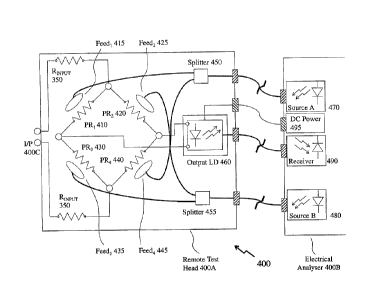
are employed in the design, evaluation, maintenance, servicing and calibration
of such
electronic and electrical control circuits, systems and devices.
[003] Within a variety of electrical measurement applications and electrical
test equipment
systems comparator bridges are employed to provide the required dynamic range,
accuracy,
and flexibility. Whilst bridge based measurement configurations remove many of
the issues
associated with achieving making measurements at accuracies of a part, or few
parts per
million, such as insensitivity to lead resistances, excellent ratio linearity,
excellent ratio
stability, and a high level of resolution they still require in many instances
that a null point be
determined where the bridge is balanced.
[004] However, this becomes increasingly difficult within electrically noisy
environments,
with modern digital multimeters, and where the desired measurement point
within the
- 1 -
Date Recue/Date Received 2020-05-07
CA 3026123
electrical system is physically difficult to access. Accordingly, in order to
address these
issues and meet the continued drive for improved accuracy in calibration,
standards, and
measurements on circuits and components means many measurements and
measurement
systems are operating at 50 parts per billion (ppb) and below to approximately
5 ppb the
inventors have established a null detector design supporting operation within
such electrically
noisy environments with physical separation of the null detector measurement
circuit from
the electrical test equipment.
[005] Other aspects and features of the present invention will become apparent
to those
ordinarily skilled in the art upon review of the following description of
specific embodiments
of the invention in conjunction with the accompanying figures.
SUMMARY OF THE INVENTION
[006] It is an object of the present invention to mitigate limitations within
the prior art
relating to null detection devices for precision electrical measurements and
precision
transducers over current ranges from lmA or less to 20kA or greater and
voltage ranges of
1V or less to 1000kV or greater and over frequency ranges from DC to hundreds
of kilohertz.
In particular, it relates to null detectors supporting precision electrical
measurements within
electrically noisy environments or at points within systems incompatible with
placement of
electrical test equipment.
[007] In accordance with an embodiment of the invention there is provided a
device
comprising:
an input port comprising an upper signal rail and a lower signal rail;
a first resistor having a first end coupled to the upper signal rail of the
input port;
a second resistor having a first end coupled to the upper signal rail of the
input port;
a third resistor having a first end coupled to the other end of the first
resistor and a second
distal end coupled to the lower signal rail of the input port;
a fourth resistor having a first end coupled to the other end of the second
resistor and a
second distal end coupled to the lower signal rail of the input port;
a first output port coupled to the other end of the first resistor and the
first end of the third
resistor;
a second output port coupled to the other end of the second resistor and the
first end of the
fourth resistor;
- 2 -
Date Recue/Date Received 2020-05-07
CA 3026123
wherein
in a first configuration the first resistor and fourth resistor are light
dependent resistors
which are each optically illuminated with first synchronized optical signals
having the same time dependent variation in illumination;
in a second configuration the second resistor and third resistor are light
dependent
resistors which are each optically illuminated with second synchronized
optical signals having the same time dependent variation in illumination;
in a third configuration the first resistor and fourth resistor are light
dependent
resistors which are each optically illuminated with third synchronized optical
signals having the same time dependent variation in illumination and the
second resistor and third resistor are light dependent resistors which are
each
optically illuminated with synchronized fourth optical signals having the same
time dependent variation in illumination.
[008] In accordance with an embodiment of the invention there is provided a
method
comprising:
providing a resistive bridge circuit comprising N light dependent resistors
(LDRs) and
M N ¨4 resistors, where both N is an integer and has a value 1 N 4;
and
driving the N light dependent resistors with R optical signals having a pulse
repetition
frequency fo and each pulse having a predetermined intensity profiles.
[009] In accordance with an embodiment of the invention there is provided a
method
comprising:
providing a measurement head;
providing a measurement circuit;
transmitting from the measurement circuit to the measurement head a plurality
of first optical
signals to the measurement head in order to at least one of power, configure,
and
control the measurement head; and
transmitting from the measurement head to the measurement circuit one or more
second
optical signals to the measurement circuit, the one or more second optical
signals
transmitting data relating to an electrical measurement performed with the
measurement head.
- 3 -
Date Recue/Date Received 2020-05-07
CA 3026123
[0010] Other aspects and features of the present invention will become
apparent to those
ordinarily skilled in the art upon review of the following description of
specific embodiments
of the invention in conjunction with the accompanying figures.
BRIEF DESCRIPTION OF THE DRAWINGS
[0011] Embodiments of the present invention will now be described, by way of
example
only, with reference to the attached Figures, wherein:
[0012] Figure 1 depicts a resistive bridge in the form of a Wheatstone bridge;
and
[0013] Figure 2 depicts a null detector employing optical isolation of the
measurement circuit
from the electrical circuit;
[0014] Figure 3 depicts a resistive bridge according to an embodiment of the
invention
employing optical driving of the resistors within the resistive bridge;
[0015] Figure 4 depicts a resistive bridge according to an embodiment of the
invention
employing optical driving of the resistors within the resistive bridge with a
measurement
head separated from the electrical test equipment;
[0016] Figure 5 depicts a resistive bridge according to an embodiment of the
invention
employing optical driving of the resistors within the resistive bridge with a
measurement
head separated from the electrical test equipment;
[0017] Figure 6 depicts schematically shaped optical pulses for linear
resistive element
variation together with offset temporal variations of first and second
resistor pairs within
resistive bridge;
[0018] Figure 7 depicts a resistive bridge according to an embodiment of the
invention
employing optical driving of the resistors within the resistive bridge with a
measurement
head separated from the electrical test equipment which includes a null
detector optically
decoupled from the electrical test equipment; and
[0019] Figure 8 depicts a resistive bridge according to an embodiment of the
invention
employing optical driving of the resistors within the resistive bridge with a
measurement
head separated from the electrical test equipment which includes a null
detector optically
decoupled from the electrical test equipment and sample-hold circuits on the
inputs.
- 4 -
Date Recue/Date Received 2020-05-07
CA 3026123
DETAILED DESCRIPTION
[0020] The present invention is directed to null detection devices for
precision electrical
measurements and precision transducers over current ranges from lmA or less to
20kA or
greater and voltage ranges of 1V or less to 1000kV or greater and over
frequency ranges from
DC to hundreds of kilohertz. In particular, it relates to null detectors
supporting precision
electrical measurements within electrically noisy environments or at points
within systems
incompatible with placement of electrical test equipment.
[0021] The ensuing description provides exemplary embodiment(s) only, and is
not intended
to limit the scope, applicability or configuration of the disclosure. Rather,
the ensuing
description of the exemplary embodiment(s) will provide those skilled in the
art with an
enabling description for implementing an exemplary embodiment. It being
understood that
various changes may be made in the function and arrangement of elements
without departing
from the spirit and scope as set forth in the appended claims.
[0022] Now referring to Figure 1 there is depicted a Wheatstone Bridge Circuit
100 for an
electrical circuit used to measure an unknown electrical resistance by
balancing two legs of a
bridge circuit wherein one leg of the bridge circuit includes an unknown
component. As
depicted the Bridge Circuit 100 comprises a first leg between node a and node
d disposed
across an input voltage, V, comprising R1 110 and R3 130 and a second leg also
disposed
between node a and node d across the input voltage, V, comprising R2 120 and
R4 140. The
output, G, being measured across nodes b and c with meter 150. Accordingly,
within the first
leg a first current i1_3 flows which is given by Equation (1) below.
Similarly, in the second
leg a second current i2_4 flows as given by Equation (2). Accordingly, the
voltage
differentials between nodes b and a or c and a are given by Equations (3) and
(4) respectively
which thereby define the output, G, by Equation (5). Accordingly, the
relationship between
G and V is defined by Equation (6). Hence, knowing R1 110, R2 120, and R4 140
allows
determination of R3 130 or where R3 130 is variable, R1 110 and R2 120 are
known then R4
140 can be found based upon adjusting R3 130 until G = 0.
= V
il-3 = (1)
Ri + R3
V
i2-4 = (2)
R2 R4
- 5 -
Date Recue/Date Received 2020-05-07
CA 3026123
VR
Vb -I/ = (3)
+ R3
VR2
(4)
a R2 + R4
G =V, ¨V, (5)
R2R3
(6)
V (R1 + R3) + (R2 R4)
[0023] Accordingly, when measuring the scenario where G 0 then the output from
the
Bridge Circuit 100 is today typically coupled to an electrical multimeter.
However, an
electrical multimeter if employed as a null detector is not an appropriate
selection as the
"zero" state of the electrical multimeter moves and therefore the apparently
determined null
will not be the null shortly thereafter as the electrical multimeter drifts.
This arises in part
from the large number of protection circuits within a multi-function
electrical multimeter that
result in a large number of leakage currents within the electrical multimeter
which impact the
measurement circuits when seeking to make an "absolute" null measurement.
Accordingly,
the meter 150 may be replaced with a null detector such as described and
depicted below in
respect of embodiments of the invention. Further, the Bridge Circuit 100 may
be replaced
with bridge circuits according to embodiments of the invention such as
described and
depicted below in respect of Figures 3 to 5 respectively.
[0024] Now referring to Figure 2 there is depicted a schematic of a Null Meter
Circuit 200
which may be an alternative option for meter 150. The Null Meter Circuit 200
provides the
user with a single function with low complexity electrical circuit and a
direct visual
indication of the voltage such that the effect of adjustment of a tunable
resistor
(potentiometer) within the Bridge Circuit 100 is visible to the user. As
depicted the Null
Meter Circuit 200 employs a photo-chopper stabilized amplifier with the
overall gain of the
amplifier being precisely controlled by negative feedback. The primary
circuits are an input
range divider 210, a photocell modulator 220, an AC amplifier 230, a
synchronous
demodulator 240, a DC amplifier 250, a meter 260, an isolation converter 270,
a neon drive
280, an 84 Hz multivibrator 290, a supply rectifier 295A, and a rectifier
filter 295B.
[0025] The input range divider 210 provides a fixed input impedance to signals
of less than a
predetermined input voltage, e.g. 1 millivolt, and allows reduction of input
signals above this
predetermined threshold. The photo-choppers 220 modulate the input signal to
the DC
- 6 -
Date Recue/Date Received 2020-05-07
CA 3026123
amplifier at 84 Hz, although an alternate frequency can be used. The drive
signal for the
photo-chopper 220 signal modulator is provided by the neon drive 280 which is
composed of
neon lamps driven alternately at a predetermined frequency, e.g. 84 Hz, by the
multi-vibrator
290. 84 Hz being a signal having a frequency asynchronous with the power line
frequencies
of 50Hz and 60Hz and power line harmonics. However, other frequencies for the
multi-
vibrator 290 may be employed. The multi-vibrator 290 also drives the supply
rectifiers 295A
which provide operating voltages for the amplifiers, the isolation converter
270 which
provides the isolated output for coupling to a chart recorder etc., and the
synchronous
demodulator 240 which demodulates the amplified DC signal. The entire
amplifier and
secondary circuits, an example of which being transformers, are surrounded by
a guard shield
which permits the use of external guard voltages.
[0026] Accordingly, the input DC signal is modulated and amplified by the AC
amplifier 230
which is a high impedance amplifier whose gain is controlled by a resistance
selected by a
range control. The amplified signal is then detected by the synchronous
demodulator driven
by the 84 Hz reference signal and detects the amplified DC signal. The
detected DC signal is
then amplified by a DC amplifier 250 whose gain is controlled by fixed
feedback. The output
signal of the DC amplifier 250 drives the meter which indicates the polarity
and magnitude of
the measured voltage, and the isolation converter 270 which drives the
isolated recorder
output. This same DC signal is also fed back to the input of the AC amplifier
230 to control
overall amplifier gain. The feedback ratio is determined by the setting of the
range control
and allows overall amplifier gain to be precisely controlled.
[0027] Whilst the Null Meter Circuit 200 employs a chopper allowing AC
amplification and
processing of the original DC measurement signal it does not have any direct
impact upon the
bridge circuit and accordingly automating any electrical potentiometer
adjustment for the
automation of electrical circuit measurements. Accordingly, the inventors have
established an
inventive bridge circuit such as depicted in Figure 3 by Bridge Circuit 300
operating
according to an embodiment of the invention employing optical driving of the
resistors within
the resistive bridge. The Bridge Circuit 300 satisfies underlying design goals
wherein the
exploitation of dual "optical chopping" provides for a balanced circuit
relative to the input
and wherein high frequency "optical chopping" provides for improved timing
information.
[0028] Within the design methodology of the inventors then two key areas are
addressed with
respect to the null detector concepts and bridge circuits employing such null
detectors.
- 7 -
Date Recue/Date Received 2020-05-07
CA 3026123
Firstly, the design methodology addresses the need to minimize crosstalk from
any
modulating signals employed within the circuit(s) so that these do not affect
the source which
the circuits are trying to balance. In order to achieve this the inventors
exploit proper shaping
of the modulating drive signal(s) such as described and depicted below in
respect of Figure 6.
Secondly, it is important to isolate modulator and detector circuits from the
output of any
instrument employing the null detector concepts and bridge circuits according
to
embodiments of the invention to minimize input bias current which is addressed
within null
detector concepts and bridge circuits by using optical isolation between the
relevant circuit
portions such as described and depicted in respect of Figures 3 to 5
respectively.
[0029] Accordingly, as depicted Bridge Circuit 300 comprises an input 300A
which is
coupled to the bridge via input resistors, RiNpuT, and an output 300B. The
bridge itself
comprises first to fourth photoresistive elements (PREs) R1 360, R2 370, R3
380, R4 390
respectively which are optically illuminated by first to fourth optical
sources LED1 310,
LED2 320, LED3 330, and LED4 340 respectively. Consider an initial case that
each of the
first to fourth optical sources LED1 310, LED2 320, LED3 330, and LED4 340
respectively
are off and that R4 is in fact an unknown. Accordingly, if LED3 330 is now
activated then the
resistance of the third PRE R3 380 will vary and the output 300B can be
monitored to
determine when a null is obtained and hence based upon the known
characteristics of the
third PRE R3 380 and the output of the third optical source LED3 330 the value
of the third
PRE R3 380 when the output is nulled can be determined. As the third optical
source LED3
330 can be varied under control of a microprocessor or microcontroller then
the null detection
process can be automated. Alternatively, different PREs can be activated or
within other
embodiments of the invention only part of the Bridge Circuit 300 employs PREs
instead of
fixed resistors or electrical potentiometers.
[0030] A photoresistive element (PSE), also known as a photoresistor, light-
dependent
resistor (LDR), or photo-conductive cell, is a light-controlled variable
resistor. The resistance
of a photoresistor decreases with increasing incident light intensity; in
other words, it exhibits
photoconductivity. A photoresistor is made of a high resistance semiconductor
such that in
the dark, a PSE can have a resistance as high as several megaohms (Me), while
in the light, a
photoresistor can have a resistance as low as a few ohms according to the
design. If incident
light on a photoresistor exceeds a certain frequency, photons absorbed by the
semiconductor
give bound electrons enough energy to jump into the conduction band. The
resulting free
- 8 -
Date Recue/Date Received 2020-05-07
CA 3026123
electrons (and their hole partners) conduct electricity, thereby lowering
resistance. The
resistance range and sensitivity of a photoresistor can substantially differ
among dissimilar
devices. Moreover, unique photoresistors may react substantially differently
to photons
within certain wavelength bands.
[0031] A photoelectric device can be either intrinsic or extrinsic. An
intrinsic semiconductor
has its own charge carriers and is not an efficient semiconductor, for
example, silicon. In
intrinsic devices the only available electrons are in the valence band, and
hence the photon
must have enough energy to excite the electron across the entire bandgap.
Extrinsic devices
have impurities, also known as dopants, added whose ground state energy is
closer to the
conduction band; since the electrons do not have as far to jump, lower energy
photons (that
is, longer wavelengths and lower frequencies) are sufficient to trigger the
device. For
example, phosphorous is one such dopant for silicon and is therefore an
example of an
extrinsic semiconductor. Alternatively, the PSE may be a photodiode or
phototransistor
although these have higher non-linearity that of an LDR.
[0032] In order to achieve a design goal of providing a balanced input bridge
circuit
according to embodiments of the invention exploit dual choppers illuminating
the PSEs and
employ pre-distortion of the optical signals coupled to the PSEs in order to
exploit the
characteristics of the PSE to establish fast response, better sensitivity etc.
as discussed below
in respect of Figure 6. However, the invention can be implemented without the
use of a
chopper. Whilst embodiments of the invention depicted in Figures 4 and 5 below
are for a
remote measurement head coupled to an electrical analyser (electrical
measurement
equipment) it would be evident that the remote test heads may be integrated
within the
electrical analyser.
[0033] Optionally, embodiments of the invention may be floated in order to
revise leakage
currents. Overall embodiments of the invention may be employed to mask the
load to the
receiver and/or remove any DC offset in the front-end and provide improved
common mode
resistance / rejection.
[0034] Accordingly, referring to Figure 4 depicts a Remote Test Head (RTH)
400A
according to an embodiment of the invention employing optical driving of the
resistors within
the resistive bridge with a measurement head separated from the electrical
test equipment.
Accordingly, the RTH 400A is coupled to the Electrical Analyser (ELEAL) 400B
via optical
connections and a single electrical link. As depicted a first optical emitter
Source A 470 is
- 9 -
Date Recue/Date Received 2020-05-07
CA 3026123
coupled from the ELEAL 400B to the RTH 400A and therein to first splitter 450
from which
the outputs are coupled to first PRE (PR1) 410 and fourth PRE (PR4) 440. A
second optical
emitter Source B 480 is coupled from the ELEAL 400B to the RTH 400A and
therein to
second splitter 455 from which the outputs are coupled to second PRE (PR2) 420
and third
PRE (PR3) 430. Also coupled from the ELEAL 400B to RTH 400A is DC Power 495
which
provides electrical power to the Output LD 460 which transmits the output
voltage across
node b and c to the ELEAL 400B. Each of the first to fourth PREs R1 410, R2
420, R3 430,
and R4 440 are coupled to their respective optical source via first to fourth
Optical Feeds,
Feed 1 415, Feed2 425, Feed3 435, and Feed4 445. The Input 400C being coupled
to the
bridge circuit via Input Resistors, Riõu, 350.
[0035] Accordingly, referring to Figure 5 depicts a Remote Measurement Head or
Remote
Test Head (RTH) 500A according to an embodiment of the invention employing
optical
driving of the resistors within the resistive bridge with a measurement head
separated from
the electrical test equipment. Accordingly, RTH 500A and ELEAL 500B are
structurally and
functionally very similar to that depicted in Figure 4 with RTH 400A and ELEAL
400B
except that now the RTH 500A is only connected via optical connections. Hence,
the
electrical connection depicted in Figure 4 is replaced with the Source C 510
within the
ELEAL 500B and DC Receiver 520 within the RTH 500A to deliver optical power
for
generating the necessary current to drive the Output LD 460. The optical power
delivery may
be a power-over-fiber system (or power-by-light) according to an industry
standard or non-
standard system.
[0036] Whilst the RTH 400A and 500A in Figures 4 and 5 are depicted as remote
from the
ELEAL 400B and 500B it would be evident that the RTH may be integrated within
the
ELEAL but would in this instance be electrically isolated and floating
relative to the ELEAL
400B or 500B.
[0037] It would be evident that depending upon the optical fiber loss
characteristics, optical
wavelength, optical power etc. required for the LDRs that the RTH 400A or 500A
in Figures
4 and 5 can be physically employed at different maximum distances from the
ELEAL such as
lm (3 feet), 2 meters (6.5 feet), 5 meters (feet), 10 meters (16 feet), 50
meters (164 feet), 100
meters (328 feet), 500m (1,640 feet) and 1000 meters (3,280 feet, 0.6 mile),
or more.
[0038] As depicted in Figure 6 with first traces 600A the outputs of Optical
Source A 470
and Optical Source B 480 as employed within ELEAL 400B and ELEAL500B in
Figures 4
- 10 -
Date Recue/Date Received 2020-05-07
CA 3026123
and 5 respectively are depicted. It is evident that these are the inverse of
one another with a
time offset & and repetition period At, the latter leading to a repetition
frequency fo = 1/At .
Accordingly, the PREs are driven by their respecting optical sources to either
increase in
resistance (reducing optical illumination) or decrease in resistance
(increasing optical
illumination). Accordingly, the output voltage is a function of optical
illumination at the
frequency, f 0 . Whilst embodiments of the invention may exploit PREs formed
from LDRs
these can be replaced with photodetectors in order to increase fo which may in
some
embodiments of the invention be beneficial to reduce noise within the
measurement.
Accordingly, as depicted a "predistortion" or shaping of the optical
illumination waveform
may lead to improved linearity in PRE resistance versus time for the
transitions whilst driving
each pair of PREs provides for no change in the load of the RTH to the input.
[0039] For example, within Figure 6 first and second traces 600B and 600C
depict the optical
illumination intensity over one cycle of the outputs of Optical Source A 470
and Optical
Source B 480 respectively which are employed within the ELEAL 400B and
ELEAL500B in
Figures 4 and 5 respectively are depicted. Optical Source A 470 being coupled
to first PRE
410 (R1) and fourth PRE 440 (R4) whilst Optical Source B 480 is coupled to
second PRE
420 *(R2) and third PRE 430 (R3). The optical intensity profile is distorted
to reflect the
linearity and time constant of the PREs such that with each cycle Optical
Source A drives the
first and fourth PREs 410 and 440 respectively linearly within the transitions
to/from a high
resistance state from an initial low resistance state and Optical Source B
drives the second
and third PREs 420 and 430 respectively linearly within the transitions
to/from a low
resistance state from an initial high resistance state. The transitions being
offset by gt
[0040] The Output LD 460 may be coupled to the output of the bridge circuit
via a low
power analog-to-digital converter (ADC) for transmission to the ELEAL.
Optionally, the
electrical link or optical link providing power to the Output LD 460 and its
associated
electronics may be eliminated and this portion of the RTH powered by a
battery.
[0041] In applications where noise performance is important then the thermal
noise of the
RTH or the bridge circuit if integrated within the ELEAL may become important.
In such
instances, the RTH or bridge circuit may be cooled. Optionally, the cooling
may be applied
through one or more Peltier elements including, for example, multi-stage
Peltier elements, or
heat pumps etc. Within other embodiments the RTH or bridge circuit may include
a
conductive plate coupled to a Dewar vessel forming part of the RTH or ELEAL
allowing the
- 11 -
Date Recue/Date Received 2020-05-07
CA 3026123
cooling to be through filling the Dewar with chlorodifluoromethane refrigerant
R-22 (-
48.6 C) or liquid nitrogen (-196 C) or exploiting subliming carbon dioxide (-
78.5 C).
[0042] Optionally, the input 400C of the RTHs 400A and 500A respectively in
Figures 4 and
or input 300A of Bridge Circuit 400A may employ protection circuitry in order
to limit the
voltage applied to the bridge portion. For example, Zener diodes may be
employed as well as
transient-voltage-suppression (TVS) diodes.
[0043] Within embodiments of the invention the optical sources, e.g. Source A
470 and
Source B 480 may be coupled to the RTHs 400A and 500A respectively by optical
fibers that
are selected in dependence upon the characteristics of the optical emitter /
source employed
such as singlemode versus multimode, operating wavelength, output power etc.
For example,
singlemode silica optical fibers may be employed for singlemode visible and
near-infrared
sources (e.g. 850nm, 1300nm, 1550nm) with typical cores of approximately lOpm;
or
multimode silica optical fibers may be employed for multimode visible and near-
infrared
sources with cores typically 50p, 62.5p, 100pm as well as 200pm, 300 pm, 365
pm, 400 pm,
550 pm, 600 pm, 800 pm, 940 pm, 1000pm. 1500pm and 2000pm for ultraviolet,
visible and
near-infrared wavelengths in silica and/or polymer. These may be terminated
with
collimating optical assemblies to provide Feed 1 415, Feed 2 425, Feed 3 435,
and Feed 4
445 with different numerical aperture, beam diameter, etc. as well as lenses
etc. Optionally, a
single optical fiber may be replaced with an array of optical fibers such as
hexagonally
packed, rectangularly packed, etc. to provide different beam profiles to
couple to the
photodiode, phototransistor or LDR. Optionally, the profile of the
illumination may be non-
uniform where the behaviour of the LDR dictates this.
[0044] These optical fibers may be coated with protective polymer coatings and
individually
cabled with additional physical protection layers such as KevlarTM and plastic
jackets and
bundled with further physical protection layers or they may be bundled within
a single
protective outer either within a single common inner tube or individually
within discrete
tubes. A single optical connector assembly may be employed in some embodiments
whilst in
other embodiments two or more optical connectors may be employed. Such
connectors may
be industry standard formats such as E-2000, FC, MIC, MPO/MTP, SC, SMA, and ST
for
example as well as many others including industry standard and custom
connectors.
[0045] Within embodiments of the invention the optical wavelength range
employed may be
a single optical wavelength (e.g. 533nm, 850nm, 1300nm etc.), multiple optical
wavelengths,
- 12 -
Date Recue/Date Received 2020-05-07
CA 3026123
a broadband emission such as from a superluminescent diode. Examples of
optical sources
may include semiconductor diodes such as light emitting diodes (LEDs), laser
diodes (LDs),
vertical cavity surface emitting lasers (VCSELs), gas lasers such as helium-
neon (633nm),
Argon ion (multiple wavelengths but commonly 488nm and 514nm), krypton laser
(multiple
wavelengths but commonly 470nm, 480nm and 520nm), helium-cadmium (442nm),
copper
vapour (510nm and 578nm), carbon dioxide (10.6 m) and solid state lasers such
as diode
pumped neodymium-doped yttrium aluminum garnet (Nd:YAG) (1.064 m).
Semiconductor
diodes may exploit InGaN (445-465nm), AlGaInP (635-760nm), GaAlAs (785-850nm),
AlGaAs (1063nm), InGaAsP (1310-650nm) as well as other semiconductors. The
figures in
brackets are common wavelengths for these semiconductors and do not reflect
the range of
wavelengths achievable through composition adjustments. Optical powers may
vary
according to laser type and design from milliwatts (mW) to hundreds of
milliwatts (100s
mW), watts (W) to hundreds of Watts and kilowatts (kW).
[0046] As depicted within Figures 3 to 5 respectively the input, e.g. Input
300A or Input
400C is depicted as a pair of contacts coupled to an upper signal rail and a
lower signal rail
(not depicted for clarity) such that the bridge circuit or RTH can float with
the input rails.
Optionally, a rail may be grounded wherein any series resistor between the
input and the
bridge circuit may be eliminated.
[0047] Within Figures 4 and 5 the four resistors are depicted as being coupled
to a pair of
optical sources each of which are optically split to couple to the pair of
resistors each optical
source is coupled to. Optionally, the splitter may be within the ELEAL rather
than the RTH
or alternatively four optical sources may be employed within the ELEAL each
coupled to one
of the LDRs wherein the four optical sources are driven as two pairs through
synchronized
drive signals.
[0048] Accordingly, whilst the descriptions above describe and depict a system
it would be
evident that a method may be implemented for configuring an electrical test
measurement by
providing a resistive bridge circuit comprised of light dependent resistors or
light dependent
diodes which is then driven through applying optical pulse signals to drive
the bridge
resistive bridge circuit. In this manner an electrical test measurement may be
performed at
point remote from the test instrument with optical isolation of the
measurement head from the
test instrument. Based upon the electrical measurement being performed a
controller within
- 13 -
Date Recue/Date Received 2020-05-07
CA 3026123
the test instrument may adjust aspects of the optical pulses applied such as
repetition
frequency, pulse profile, and upper / lower limits of illumination.
[0049] Within the descriptions above in respect of embodiments of the
invention with respect
to a system comprising a resistive bridge circuit in conjunction with a null
detector no
specific distinction has been made as to whether the devices and/or systems
exploiting
embodiments of the invention receive direct current (DC) or alternating
current (AC) signals.
Typically, within the prior art such resistive bridge circuits and null
detectors are employed
upon DC signals. However, the inventors have established variants of the
system which allow
for the systems and/or devices according to embodiments of the invention to
operate with AC
signals.
[0050] According to an embodiment of the invention devices and/or systems
according to
embodiments of the invention may exploit built in synchronization within the
devices and/or
systems, for example via hardware or firmware, so that two input AC signals,
whether current
or voltage, can be synchronized prior to comparing the signals via the
internal optical bridge
and determining the null point. The two input AC signals may be the same
frequency, or they
may have different frequencies, but their currents or voltages may be
compared.
[0051] With respect to determining which portion of the applied AC signal is
employed to
determine the AC null point then this may be any portion of the AC signal as
defined by the
hardware or firmware. Optionally, the portion of the AC signal employed may be
varied
within other devices and/or systems according to embodiments of the invention
through a
selection with respect to the device and/or system itself or through a
selection by an external
controller in communication with a processor forming part of the device and/or
system.
Accordingly, the portion of the AC signal may be the positive amplitude
magnitude, negative
amplitude magnitude, or other portions of the AC signal. Further, within other
embodiments
of the invention the determination of an AC signal with respect to the null
point with respect
to the cross-over position of the synchronized signal(s), or unsynchronized
signal(s) then the
devices and/or systems may be configured to one determination method or they
may provide
configurability with respect to the determination method. Examples of
determination methods
may comprise a zero crossing method or a root-mean-square (RMS) method or
other
predetermined portions.
[0052] Within embodiments of the invention a sample-and-hold circuit may be
employed for
both DC and AC signals so that the null point is determined based on the
signal "released" by
- 14 -
Date Recue/Date Received 2020-05-07
CA 3026123
the sample-and-hold circuit. It would be evident that therefore a sample-and-
hold circuit is
provided for each input signal. One such sample-and-hold circuit may be based
upon the use
of a capacitor based circuit which would charge up based on the AC, or DC
signal.
Accordingly, the capacitance charge level could then be fed into the optical
bridge and
compared. Beneficially, this would allow an AC signal to be compared with or
without
having the two input AC circuits synchronized.
[0053] Now referring to Figure 7 there is depicted a resistive bridge
according to an
embodiment of the invention employing optical driving of the resistors within
the resistive
bridge with a Measurement Head 700A separated from the Electrical Analyser
700B. The
Measurement Head 700A includes a null detector 720 which is coupled to the
Output LD 460
so that it is optically decoupled from the electrical test equipment. The Null
Detector 720 is
coupled to a Sync Circuit 740 within the Measurement Head 700A which is
coupled to a DC
& Data circuit 730 within the Electrical Analyser which now provides DC power
to the Sync
740 and Null Detector 720 together with the Output LD 460 but also provides
clock and/or
data signals to the Sync 740. Within an embodiment of the invention the DC &
Data circuit
730 is electrically coupled between the Electrical Analyser 700B and the
Remote Test Head
700A whilst within other embodiments of the invention the connections may be
optical for
data signals and electrical for DC power or optical for both power and data
signals.
[0054] Now referring to Figure 8 there is depicted a resistive bridge
according to an
embodiment of the invention employing optical driving of the resistors within
the resistive
bridge with a Measurement Head 800A separated from the Electrical Analyser
800B. The
Measurement Head 800A includes a null detector 720 which is coupled to the
Output LD 460
so that it is optically decoupled from the electrical test equipment. The Null
Detector 720 is
coupled to a Sync Circuit 740 within the Measurement Head 700A which is
coupled to a DC
& Data circuit 730 within the Electrical Analyser which now provides DC power
to the Sync
740 and Null Detector 720 together with the Output LD 460 but also provides
clock and/or
data signals to the Sync 740. Additionally, the Inputs 400C are now coupled to
first and
second sample-hold circuits SH1 810 and 5H2 820 respectively which are coupled
to the
Sync Circuit 740 so that these can be "gated" or clocked to provide the
signals to the resistive
bridge as described above. Within an embodiment of the invention the DC & Data
circuit 730
is electrically coupled between the Electrical Analyser 800B and the Remote
Test Head 800A
- 15 -
Date Recue/Date Received 2020-05-07
CA 3026123
whilst within other embodiments of the invention the connections may be
optical for data
signals and electrical for DC power or optical for both power and data
signals.
[0055] Accordingly, the resistive bridge within some embodiments of the
invention may be
decoupled from the electrical test equipment with the optical connections
between the
measurement head and the electrical test equipment and the null detector is
within the
electrical test equipment.
[0056] Accordingly, the resistive bridge and null detector within some
embodiments of the
invention may be decoupled from the electrical test equipment with the optical
connections
between the measurement head and the electrical test equipment with full
optical decoupling
for all signals including any DC power. In other embodiments of the invention
the optical
decoupling may be for all AC signals with only DC electrical power between the
measurement head and electrical test equipment. Within other embodiments of
the invention
the optical decoupling may be for all optical signals to the resistive bridge
and from an
integrated null detector with only DC power and AC data being electrically
provided between
the measurement head and the electrical test equipment. Optionally, data
signals and/or DC
power may also be coupled to the measurement head using one or more wireless
interfaces
according to embodiments of the invention.
[0057] Specific details are given in the above description to provide a
thorough
understanding of the embodiments. However, it is understood that the
embodiments may be
practiced without these specific details. For example, circuits may be shown
in block
diagrams in order not to obscure the embodiments in unnecessary detail. In
other instances,
well-known circuits, processes, algorithms, structures, and techniques may be
shown without
unnecessary detail in order to avoid obscuring the embodiments.
[0058] Implementation of the techniques, blocks, steps and means described
above may be
done in various ways. For example, these techniques, blocks, steps and means
may be
implemented in hardware, software, or a combination thereof. For a hardware
implementation, the processing units may be implemented within one or more
application
specific integrated circuits (ASICs), digital signal processors (DSPs),
digital signal
processing devices (DSPDs), programmable logic devices (PLDs), field
programmable gate
arrays (FPGAs), processors, controllers, micro-controllers, microprocessors,
other electronic
units designed to perform the functions described above and/or a combination
thereof.
- 16 -
Date Recue/Date Received 2020-05-07
CA 3026123
[0059] Also, it is noted that the embodiments may be described as a process
which is
depicted as a flowchart, a flow diagram, a data flow diagram, a structure
diagram, or a block
diagram. Although a flowchart may describe the operations as a sequential
process, many of
the operations can be performed in parallel or concurrently. In addition, the
order of the
operations may be rearranged. A process is terminated when its operations are
completed, but
could have additional steps not included in the figure. A process may
correspond to a method,
a function, a procedure, a subroutine, a subprogram, etc. When a process
corresponds to a
function, its termination corresponds to a return of the function to the
calling function or the
main function.
[0060] The foregoing disclosure of the exemplary embodiments of the present
invention has
been presented for purposes of illustration and description. It is not
intended to be exhaustive
or to limit the invention to the precise forms disclosed. Many variations and
modifications of
the embodiments described herein will be apparent to one of ordinary skill in
the art in light
of the above disclosure. The scope of the invention is to be defined only by
the claims
appended hereto, and by their equivalents.
[0061] Further, in describing representative embodiments of the present
invention, the
specification may have presented the method and/or process of the present
invention as a
particular sequence of steps. However, to the extent that the method or
process does not rely
on the particular order of steps set forth herein, the method or process
should not be limited to
the particular sequence of steps described. As one of ordinary skill in the
art would
appreciate, other sequences of steps may be possible. Therefore, the
particular order of the
steps set forth in the specification should not be construed as limitations on
the claims. In
addition, the claims directed to the method and/or process of the present
invention should not
be limited to the performance of their steps in the order written, and one
skilled in the art can
readily appreciate that the sequences may be varied and still remain within
the scope of the
present invention.
- 17 -
Date Recue/Date Received 2020-05-07