Note: Descriptions are shown in the official language in which they were submitted.
CA 03029898 2018-12-21
1 NEUROSTIMULATOR AND METHOD FOR DELIVERING A STIMULATION IN RESPONSE TO
2 A PREDICTED OR DETECTED NEUROPHYSIOLOGICAL CONDITION
3 TECHNICAL FIELD
4 [0001] The following relates generally to neurostimulators; and more
particularly to a wearable
or implantable neurostimulator and a method for monitoring, diagnosing and
responding to
6 neurophysiological disorders or conditions.
7 BACKGROUND
8 [0002] Micro-scale chips can be implanted or otherwise positioned in situ
on a subject to
9 measure target analytes. Integrating measurement functions of laboratory
techniques into
micro-scale implantable/wearable chips provides added convenience and accuracy
of
11 measurement. Excessive power draw from components of
implantable/wearable micro-scale
12 chips can limit utility given that power available to micro-scale chips
is limited by either battery
13 capacity or by the budget of a wireless power link. Further, excessive
power consumption in
14 such a chip may cause tissue damage to the surrounding area.
[0003] Several chips providing brain-neural interfaces have been reported in
the literature; a
16 handful of these are equipped with on-chip signal processing. However,
the detection
17 techniques of these chips are generally amplitude-based, resulting in
late detection of
18 neurophysiological events. For events such as epileptic seizures, a late
detection makes it
19 impossible to abort the seizures using responsive stimulation. Further,
the published chips
generally use OpAmp-based front-ends that can only tolerate up to a certain
amplitude before
21 being saturated. To combat this saturation, the published chips either
use AC-coupled inputs
22 which result in large recording channel area, or use DC-coupled front-
ends with digitally-
23 assisted feedback systems that can only reject up to 50 mV, which is
not sufficient in many
24 cases.
[0004] The published neuro-stimulators are generally only capable of
stimulating either a fixed
26 pulse or at best a biphasic semi-programmable pulse train that is time-
invariant and not subject-
27 specific. These stimulators either have no programmability or require
long stimulation parameter
28 adjustment by a clinician for each new subject as well as frequent
tuning over time for the same
29 subject. Commercially-available neurostimulators are either open-loop
(frequent periodic
1
CA 03029898 2018-12-21
1 stimulation with no detection) or closed-loop with ineffective detection
algorithms that result in
2 very high false positive rate and inability to pre-emptively abort
seizures due to late detection.
3 SUMMARY
4 [0005] In an aspect, there is provided a neurostimulator, the
neurostimulator implantable or
wearable on a subject, the neurostimulator comprising: a power circuit for
providing electrical
6 power to the neurostimulator; a recording array having a plurality of
electrodes for recording a
7 plurality of neurophysiological signals corresponding to a plurality of
sites of the subject; a
8 signal processor configured to: determine a phase synchrony among the
neurophysiological
9 signals; and associate selected phase synchrony calculations with the
prediction or detection of
a neurological or neurophysiological condition; and one or more stimulators
for delivering to the
11 subject a stimulation in response to the predicted or detected
condition.
12 [0006] In a particular case, the responsive stimulation comprises any
one or more of an
13 electrical charge, electrical current, electrical voltage, optical
signal, chemical agent and
14 temperature controlling signal.
[0007] In another case, the power circuit comprises a wireless inductive link
permitting a
16 receiver coil to be located remotely from the neurostimulator.
17 [0008] In yet another case, the recording array records signals by
electroencephalography,
18 electrocardiography, electromyography, or a combination thereof.
19 [0009] In yet another case, the recording array is configured to record
either current or voltage.
[0010] In yet another case, the neurostimulator further comprises a digitizer,
and the recording
21 array is linked to the digitizer for digitizing the neurophysiological
signals.
22 [0011] In yet another case, the digitizer comprises an in-channel AZ or
A2Z neural analog-to-
23 digital converter.
24 [0012] In yet another case, the signal processor is a digital signal
processor.
[0013] In yet another case, the recording array comprises sixty four channels.
26 [0014] In yet another case, the recorded signals are modulated by a 1-
bit waveform, wherein
27 the waveform is 1 when sin(wot)/cos(wot)>1 and 0 when
sin(wot)/cos(wot)<0.
2
CA 03029898 2018-12-21
1 [0015] In yet another case, the stimulators comprise a waveform generator
configured to
2 generate an arbitrary current-mode waveform to be applied to a subset of
the stimulators.
3 [0016] In yet another case, the arbitrary current-mode waveform is
generated with a spatio-
4 temporal profile determined specifically for the subject.
[0017] In yet another case, the determination of the spatio-temporal profile
comprises a one-
6 sided simultaneous perturbation stochastic approximation (SPSA), wherein
for any particular
7 stimulation the one-sided SPSA applies exactly one sampling of the phase
synchrony to
8 compute a gradient approximation.
9 [0018] In yet another case, the waveform generator provides an analog in-
channel multiplier for
the recording array.
11 [0019] In yet another case, the waveform generator provides the signal
and its derivative for
12 use in the calculation of phase synchrony.
13 [0020] In yet another case, the subset of the stimulators is selected
based on one or more
14 machine learning algorithms to provide optimal stimulation amplitude.
[0021] In another aspect, there is provided a method for neurostimulation
comprising: applying
16 a recording array to a subject; recording, by the recording array, a
plurality of neurophysiological
17 signals corresponding to plurality of sites of the subject; determining
a phase synchrony among
18 the neurophysiological signals; associating selected phase synchrony
calculations with the
19 prediction or detection of a neurological or neurophysiological
condition; and delivering to the
subject, by one or more stimulators, a stimulation in response to the
predicted or detected
21 condition.
22 [0022] In a particular case, the stimulators apply the stimulation
comprising any one or more of
23 an electrical charge, electrical current, electrical voltage, optical
signal, chemical agent and
24 temperature controlling signal.
[0023] In another case, the recording array records signals by
electroencephalogram,
26 electrocardiograms, electromyography, or a combination thereof.
27 [0024] In yet another case, the recording array is configured to record
either current or voltage.
3
CA 03029898 2018-12-21
1 [0025] In yet another case, the method further comprising digitizing the
neurophysiological
2 signals prior to calculating the phase synchrony.
3 [0026] In yet another case, the digitizing comprises applying an in-
channel AZ or LI2Z neural
4 analog-to-digital converter.
[0027] In yet another case, the recording array comprises sixty four channels.
6 [0028] In yet another case, the recorded signals are modulated by a 1-bit
waveform, wherein
7 the waveform is 1 when sin(wot)/cos(wot)>1 and 0 when
sin(wot)/cos(wot)<0.
8 [0029] In yet another case, the stimulation comprises generating and
applying an arbitrary
9 current-mode waveform to a subset of the stimulators.
[0030] In yet another case, the arbitrary current-mode waveform is generated
by a waveform
11 generator using a spatio-temporal profile determined specifically for
the subject.
12 [0031] In yet another case, the determination of the spatio-temporal
profile comprises a one-
13 sided simultaneous perturbation stochastic approximation (SPSA), wherein
for any particular
14 stimulation the one-sided SPSA applies exactly one sampling of the phase
synchrony to
compute a gradient approximation.
16 [0032] In yet another case, the waveform generator provides an analog in-
channel multiplier for
17 the recording array.
18 [0033] In yet another case, the waveform generator provides the signal
and its derivative for
19 use in the calculation of phase synchrony.
[0034] In yet another case, the subset of the stimulators is selected based on
one or more
21 machine learning algorithms to provide optimal stimulation amplitude.
22 [0035] These and other aspects are contemplated and described herein. It
will be appreciated
23 that the foregoing summary sets out representative aspects of
neurostimulators and methods to
24 assist skilled readers in understanding the following detailed
description.
DESCRIPTION OF THE DRAWINGS
4
CA 03029898 2018-12-21
1 [0036] A greater understanding of the embodiments will be had with
reference to the Figures, in
2 which:
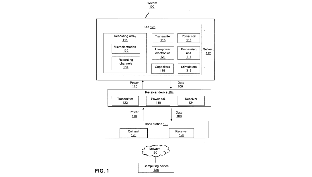
3 [0037] Figure 1 shows a block diagram of a system for in situ monitoring,
diagnostics and
4 responsive stimulation of various neurophysiological disorders;
[0038] Figure 2 shows flowchart for a method for in situ monitoring,
diagnostics and responsive
6 stimulation of various neurophysiological disorders;
7 [0039] Figure 3 shows application of the system of Figure 1 for selective
imaging of the
8 concentrations of potassium (K+) ions over sodium (Na+) ions;
9 [0040] Figure 4 shows a two-stage inductive powering system for in situ
monitoring, diagnostics
and responsive stimulation of various neurophysiological disorders;
11 [0041] Figure 5 shows a three-stage inductive powering system for in
situ monitoring,
12 diagnostics and responsive stimulation of various neurophysiological
disorders;
13 [0042] Figure 6 shows a block diagram of an implantable/wearable die of
a system for in situ
14 monitoring, diagnostics and responsive stimulation of various
neurophysiological disorders;
[0043] Figure 7 shows possible inter-channel phase synchrony in a certain
region of the
16 brain(arrowed) and other regions(dots);
17 [0044] Figure 8 shows a digitally-assisted analog front-end of a
recording channel;
18 [0045] Figure 9 shows simplified schematics of incremental design of a
A21-based front ends of
19 recording channels of the neurostimulator die;
[0046] Figures 10 further shows a simplified schematic of a A2Z-based front
end of recording
21 channels of the die;
22 [0047] Figure 11 shows circuit schematics of the A2Z-based front end of
recording channels of
23 the die;
24 [0048] Figure 12 shows a circuit of the front end of recording channels
of the die for achieving a
dual mode operation wherein the front-end is configured to record both
electrical current and
26 voltage;
5
CA 03029898 2018-12-21
1 [0049] Figure 13 shows a block diagram of the die comprising combined
recording and
2 stimulator channels;
3 [0050] Figure 14 shows a stimulator circuit for the die;
4 [0051] Figure 15 shows an embodiment of the recording channels of the die
wherein CMOS
charge pumps of the stimulator circuit are utilized in the front end of
recording channels;
6 [0052] Figure 16 shows a block diagram of a power management circuit that
generates supply
7 voltages from the energy received by power coil, as well as a data
receiver that receives and
=
8 decodes configuration commands from the wireless link;
9 [0053] Figure 17 shows possible area scalability of the die with the
,6,2Z-based design compared
to the scalability of a die comprising a traditional AC-coupled recording
channel components;
11 [0054] Figure 18 shows circuit diagrams of an electrical current
recording channel minimized in
12 size and power consumption by merging circuit blocks;
13 [0055] Figure 19 shows an implementation of a digital multiplication
operation performed on the
14 output of a delta sigma ADC of a recording channel of the die after a
decimation filter;
[0056] Figure 20 shows the replacement of the 16-bit coefficient
multiplication of Figure 19 by a
16 1-bit XOR;
17 [0057] Figure 21 illustrates decibels relative to full scale ("dBFS")
against frequency for a tone
18 signal after down-conversion by an ideal sine wave signal;
19 [0058] Figure 22 illustrates dBFS against frequency for a tone signal
after down-conversion by
a squarewave approximation of a sinewave signal;
21 [0059] Figure 23 shows a zero-kickback comparator circuit used to
implement the delta-sigma
22 .. ADC in the proposed recording channel;
23 [0060] Figure 24 shows dynamic logic buffers and other pulse shaping
circuits necessary for
24 connecting the comparator output to clocks; and
[0061] Figure 25 shows a block diagram of the charge pump to implement the I-
DAC in the
26 feedback.
6
CA 03029898 2018-12-21
1 DETAILED DESCRIPTION
2 [0062] For simplicity and clarity of illustration, where considered
appropriate, reference
3 numerals may be repeated among the Figures to indicate corresponding or
analogous
4 elements. In addition, numerous specific details are set forth in order
to provide a thorough
understanding of the embodiments described herein. However, it will be
understood by those of
6 ordinary skill in the art that the embodiments described herein may be
practised without these
7 specific details. In other instances, well-known methods, procedures and
components have not
8 been described in detail so as not to obscure the embodiments described
herein. Also, the
9 description is not to be considered as limiting the scope of the
embodiments described herein.
[0063] Various terms used throughout the present description may be read and
understood as
11 follows, unless the context indicates otherwise: "or" as used throughout
is inclusive, as though
12 written "and/or"; singular articles and pronouns as used throughout
include their plural forms,
13 and vice versa; similarly, gendered pronouns include their counterpart
pronouns so that
14 pronouns should not be understood as limiting anything described herein to
use,
implementation, performance, etc. by a single gender. Further definitions for
terms may be set
16 out herein; these may apply to prior and subsequent instances of those
terms, as will be
17 understood from a reading of the present description.
18 [0064] Any module, unit, component, server, computer, terminal or device
exemplified herein
19 that executes instructions may include or otherwise have access to computer
readable media
such as storage media, computer storage media, or data storage devices
(removable and/or
21 non-removable) such as, for example, magnetic disks, optical disks, or
tape. Computer storage
22 media may include volatile and non-volatile, removable and non-removable
media implemented
23 in any method or technology for storage of information, such as computer
readable instructions,
24 data structures, program modules, or other data. Examples of computer
storage media include
RAM, ROM, EEPROM, flash memory or other memory technology, CD-ROM, digital
versatile
26 disks (DVD) or other optical storage, magnetic cassettes, magnetic tape,
magnetic disk storage
27 or other magnetic storage devices, or any other medium which can be used
to store the desired
28 information and which can be accessed by an application, module, or
both. Any such computer
29 storage media may be part of the device or accessible or connectable
thereto. Further, unless
the context clearly indicates otherwise, any processor or controller set out
herein may be
31 implemented as a singular processor or as a plurality of processors. The
plurality of processors
32 may be arrayed or distributed, and any processing function referred to
herein may be carried out
7
CA 03029898 2018-12-21
1 by one or by a plurality of processors, even though a single processor
may be exemplified. Any
2 method, application or module herein described may be implemented using
computer
3 readable/executable instructions that may be stored or otherwise held by
such computer
4 readable media and executed by the one or more processors.
[0065] Embodiments described herein generally provide a millimetre scale
package-free
6 complementary metal¨oxide¨semiconductor ("CMOS") chip (referred to below
as "die") for the in
7 situ (on-site) high-spatial resolution measurement of electrochemically
detectable analytes
8 (such as Na+, K+, Ca++ and glucose, for example), and for responsive
stimulation by electrode
9 stimulators to abort a neurophysiological event before its onset.
Embodiments of the die
comprise an electrode array and an associated recording channel array for
measuring recording
11 signals relating to target analytes.
12 [0066] More particularly, the embodiments provide a closed loop
responsive neurostimulator
13 device that is capable of recording both electrical voltages and
currents, on-chip signal
14 processing and arbitrary waveform electrical (current or voltage) and
optical stimulation. The
voltage recording is used for monitoring neurophysiological signals such as
EMG, ECG and
16 brain EEG and ECoG. The current recording capability enables
applications such as Na+ and
17 K+ ion concentration monitoring (which may be used for neurological
event detection),
18 impedance spectroscopy, and cyclic voltammetry. Signal processing is
described wherein
19 phase is used as one of the features for neurological event detection.
Signal processing
techniques may include machine learning analysis. Further, optimal patient-
specific time-variant
21 electrical stimulation may be implemented.
22 [0067] The die comprises recording channels providing a hardware
implementation of
23 synchrony-based neurological event detection (such as early epileptic
seizure detection). The
24 described switched-capacitor-based implementation prevents amplifier
saturation from high
input signal amplitudes or DC offset variations by recording rail-to-rail
signal amplitude/DC-
26 offset variations. This ensures the die is useful not only for
neurological monitoring (e.g.
27 electroencephalogram "EEG"), but also for other technologies that
provide a measurable signal
28 array, such as electromyography ("EMG"), electrocardiograms ("ECG"),
etc.).
29 [0068] The die also provides stimulators for responsive stimulation
requiring minimal tuning of
stimulation parameters over time and from subject to subject. The die
comprises a processing
31 unit communicatively coupled to both the stimulators and to the
recording channels, that may
8
CA 03029898 2018-12-21
1 implement a machine-learning based technique for feature detection from
recorded signals that
2 auto-adjusts a stimulation profile to optimal values for each new subject
over time.
3 [0069] An inductive power transfer system and a short-range communication
circuit power and
4 communicate with the die simultaneously. Due to circuits used in design
of the front-end of the
recording channels and a local signal processing unit, total power consumption
fits within the
6 inductive power transmission link budget.
7 [0070] The die may thus be fully-implantable, wireless and capable of
early detection of
8 neurophysiological events (such epileptic seizure) .The die may further
provide responsive
9 subject-specific stimulation.
[0071] Further, embodiments of the recording channel of the die are described
which may
11 minimize size and power consumption by multiplying recording channel
outputs by a 1-bit
12 waveform ("1" when sin(w0t)/cos(w0t)>1 and "0" when sin(wot)/cos(wot)<O)
utilizing a XOR gate,
13 instead of high-resolution sin(wot) and cos(wot) waveforms. The single
XOR gate replaces the
14 many digital logic gates of conventional impedance spectroscopy ("IS")
circuits.
[0072] Further, embodiments described herein provide a zero-hysteresis
comparator circuit
16 which may reduce or eliminate signal distortion. This circuit may reduce
naturally occurring
17 hysteresis in the comparator by isolating the output of the comparator
from its input.
18 [0073] Referring now to Fig. 1, a block diagram of a system 100 for in
situ monitoring,
19 diagnostics, and responsive stimulation of various neurological or
neurophysiological disorders
or conditions is shown. The system 100 comprises a base station 102, an
optional receiver
21 device 104 and a die 106, the components and functionality of which will
be described in more
22 detail below. In use, the die 106 may be positioned in situ for
measurement of target analytes of
23 a subject 112.
24 [0074] The die 106 comprises a recording array 114 comprising associated
recording channels
134 for recording signals relating to electrochemical reactions occurring at
an electrode-tissue
26 interface, such as interactions with chemically bonded analytes, and
digitizing the signals for
27 transmission. More particularly, die 106 may comprise microelectrodes
132. In some cases,
28 along at least one of its surfaces a plurality of microelectrodes 132
are used for bonding
29 chemically with targeted analytes when the die is positioned at a
location of interest of a subject
112, in situ, and activated. The die further comprises a transmitter unit 115
for transmitting data
9
CA 03029898 2018-12-21
1 relating to the recorded sensor signals, a power coil 116 for receiving
energy (and possibly
2 control signals and a clock) by magnetic induction from the receiver
device 104 or base station
3 102, low-power electronics 121, and a bank of capacitors 119 for storing
energy on the die to
4 power the low-power electronics 121. The die may comprise a processing
unit 111 for
processing recorded signals locally at the die; and stimulators 318 (which may
be any one or
6 more of electrical/optical/chemical/temperature-based), triggered upon
the prediction/detection
7 of the onset of a target neurophysiological event from the recording
signals.
8 [0075] The receiver device 104 comprises a transmitter 122, a receiver
124 and a power coil
9 118. The base station 102 comprises a receiver 126 and a power coil 120.
The die 106, receiver
104 and base station 102 comprise other components as set out in more detail
below with
11 reference to particular embodiments.
12 [0076] In use, the die 106 transmits data comprising recorded signals
(illustrated as block 108)
13 to the receiving device 104, and receives power therefrom (illustrated
as block 110). Similarly,
14 the receiver device 104 transmits data received from the die to the base
station 102 and
receives power therefrom, as illustrated by blocks 109 and 110, respectively.
The base station
16 102 may be communicatively linked over a wired or wireless network 130
with a computing
17 device 128 for processing received data. Optionally, data may be
processed locally at the base
18 station 102 if the base station comprises hardware for processing the
data, or at the die 106.
19 Alternatively, the die 106 may be directly linked with the base station
102, and the
communication of power and data may occur over a wired connection.
21 [0077] Referring now to Fig. 2, a method 220 for in situ monitoring,
diagnostics and responsive
22 stimulation of various neurophysiological disorders is shown. According
to the method 220 at
23 block 202 the die 106 is positioned at a location of interest in or on a
subject 112. This location
24 might, for example, be adjacent to the subject's eye, brain, or other
tissue for which analyte
monitoring is desired. At block 204 the die is activated by the placement of a
receiver device
26 104 or base station 102 nearby and the transmission of power to the die.
At block 206 the die
27 records signals responsive of electrochemical reactions occurring at the
particular location
28 making contact with the die's microelectrodes, such as signals
indicative of the concentration of
29 target analytes, such as ions, molecules, or microorganisms. More
particularly, once the die is
activated at block 204, the recording channels 134 of the recording module
array 114
31 periodically record the electric charge accumulation on their
corresponding microelectrode 132
32 and convert them to digital data. At block 208, the die may send out the
recorded data using
CA 03029898 2018-12-21
1 radio-frequency ("RF") waves via the transmitter unit 115 to the receiver
104 (or directly to the
2 base station 102), positioned nearby, and preferably situated as close as
possible to the die
3 106. At block 210, the data comprising the recorded signals may be
buffered and re-transmitted
4 to another RF receiver unit (referred to generally as base station 102)
which could be farther
away (e.g. meters or further) from the die 106 and the first receiver 104. At
block 212, the data
6 may be stored in memory at the receiver device 104 (or base station 102,
if re-transmitted at
7 block 210). At block 214, the data may be processed, either at the
receiver device 104, base
8 station 102 or at a communicatively linked computing device, depending on
the configuration of
9 the system. In some embodiments, the data may be processed locally at the
die at a processing
unit 111. At block 216, based on the processed data, prediction/detection of
the onset of a
11 target neurophysiological event may trigger
electrical/optical/chemical/temperature-based
12 stimulators 318.
13 [0078] Referring now to Fig. 3, a particular application of the method
220 is shown, applying the
14 in situ CMOS die 106 for selective imaging of concentrations of
potassium (K+) ions over
sodium (Na+) ions across the implanted region on the cortex of a free-moving
subject 112. The
16 die surface takes a 2-dimensional image of analyte concentration profile
by simultaneously
17 conducting impedance spectroscopy at all individual microelectrode sites
in parallel and
18 converting the resulting signals to digital words at the electrode
location in the die. The digital bit
19 stream created from all the microelectrodes data - i.e. impedance
spectroscopy information from
all individual on-chip nnicroelectrodes in the die - is transmitted wirelessly
outside the body to a
21 receiver 104. Specifically, a miniature radio comprising a transmitter
on the die communicates
22 the recorded information to the receiving device 104. As illustrated,
the receiving device 104
23 may be worn and may be placed on the surface of the subject's skin 112
as close as practically
24 possible to the implanted die. The receiving device 104 may thus be
constructed as a flexible
patch. The wearable receiving device 104 then re-transmits this information by
a more powerful
26 radio to a base station 102 such as a handheld unit or a PC for analysis
and display and/or
27 permanent storage. The ionic concentrations provided from the imaging
information may be
28 useful for the diagnosis and possible abortion of seizure onsets in
subjects with intractable
29 epilepsy.
[0079] The neurological application provided in Fig. 3, and described in some
instances below,
31 is merely illustrative. It is contemplated that the die 106 could also
be used for in situ
32 measurement in other locations of interest and of other target analytes.
For example, the die
33 could be fabricated into a contact lens for measurement of glucose
levels or other analytes
11
CA 03029898 2018-12-21
1 along the surface of the eye. Description below of particular embodiments
for neurological
2 imaging are provided for illustration and are not intended to be limiting
of contemplated
3 applications.
4 [00801 Referring now to Figs. 4 to 5, shown therein are further
embodiments of systems 200,
250 for in situ monitoring, diagnostics and responsive stimulation of various
neurophysiological
6 disorders. The embodiments shown illustrate a two stage system 200 and a
three stage system
7 250 used to wirelessly link the die 106 to the base station 102.
Depending on the application,
8 the die 106 can communicate directly with the base station 102 in a two
stage system illustrated
9 in Fig. 4, comprising stages L1 and L2. Alternately, according to a three
stage system
comprising stages L1, L2 and L3, a receiving device 104 may be provided at a
second
11 intermediary stage L2, to link with the base station 102, as shown in
Fig. 5.
12 [00811 Describing now more particularly the components and functionality
of the die, in an
13 embodiment the die 106 comprises a recording array 114 comprising an
array of electrodes
14 132, such as a 32x32 array, with a dedicated recording channel 134
fabricated underneath each
electrode. The power coil 116 may be fabricated around the electrode array.
Low-power
16 electronics 121 comprising components for peripheral clock generation
and data processing, as
17 well as power management circuits may further be fabricated around the
recording channel 134
18 array, underneath the energy harvesting power coil 116. The low-power
electronics 121 may
19 comprise circuit components, such as a delay-locked loop ("DLL"), an
integrated digital-analog
converter ("DAC"), a timing sequence generator, a 13-bit counter, a divide-by-
8 frequency
21 divider, a decoder, an amplitude-modulated demodulator ("AM
Demodulator"), an analog to
22 digital converter ("ADC"), a low-pass filter ("LPF'"), a rectifier, a
backscatter modulator and a
23 multiplexer A storage capacitor bank may also be provided. With respect
to the power
24 management circuit of electronics 121, electric energy to power the die
106 microsystem may
be generated by an integrated rectifier which can convert AC voltage induced
in the energy
26 harvesting power coil 116 into supply voltages, such as at 0.6V and
1.2V. Optionally, the 0.6V
27 voltage may be used to power the all the digital circuits and the 1.2V
supply can be used to
28 power analog signal processing and the RF front-end data communication
circuits. Other
29 components of the die are contemplated, as described in more detail
below. For example, in
some embodiments, the die includes a signal processing unit, power management
circuit,
31 wireless transmitters (UWB and FSK) and FIR Filters (such as 8 64-tap
FIR Filters).
12
CA 03029898 2018-12-21
1 [0082] More particularly, the recording channels 134 are organized in the
form of an array 114
2 in the center of the die underneath the electrodes 132. The area of the
array may be surrounded
3 on a top layer by the power coil 116. With regards to the electrodes 132,
each column may
4 comprise sixty four working electrodes and one reference electrode
running alongside the
column of working electrodes. During operation, the reference electrode may be
driven by a
6 periodic voltage signal (sinusoid, ramp, or sawtooth) while voltage of
all the working electrodes
7 may be held at a constant value (of approximately 300mV to 500mV). During
a current-
8 recording mode of operation, the current flowing into the working
electrode as a result of its
9 potential difference with the reference electrode may be recorded by a
recording channel front-
end operating essentially as a transimpedance amplifier. The output of the
recording channel
11 may be converted to digital words read by the array readout circuit
after in-channel bandpass
12 filtering.
13 [0083] Describing in more detail a mode of operation of a particular
embodiment of the die 106,
14 once the die is activated at block 204 of method 220, the channels 134
of the recording module
array 114 periodically record the electric charge accumulation on their
corresponding
16 nnicroelectrode 132 and convert them to digital data, such as 16-bit
digital words which can be
17 stored in 16 D-flip-flops fabricated inside each channel. After each
conversion, the 16-bit
18 content of all the channels may be extracted and serialized by a readout
circuit (such as by a
19 column decoder and row multiplexer). The column decoder may switch the
content of the
channels onto 16-bit bus lines running along the rows of the array. A
multiplexer may
21 sequentially read out the row buses once they are switched onto the D-
flip-flops inside the
22 individual channels. The multiplexer may produce two serial outputs
corresponding to the less
23 significant and the more significant bytes of channels' 134 data words.
The serial outputs of the
24 multiplexer may be fed into the on-chip radio transmitter which may send
the data out to the
base station 102 (in the two-stage setup), or the intermediate stage 104 (in
the three-stage
26 setup. This mode of operation thus multiplexes data for sending as an
output. In another mode
27 of operation, the data could also be sent to an on-chip signal
processing unit (which could
28 process the data for neurological event detection), and then the result
of processing could be
29 transmitted wirelessly to a receiver, which could be worn on the user's
body or hand-held.
[0084] As described above, the energy to power the CMOS die 106 is delivered
via magnetic
31 induction from the receiving device 104 or base station 102 (illustrated
as element 110). In the
32 two stage system 200, the base station 102 generates an alternating
magnetic field in power
33 coil 120 which is induced into an integrated power coil 116 in the die.
The magnetic energy is
13
CA 03029898 2018-12-21
1 then converted to electric energy which is stored on a bank of capacitors
119 on the die to
2 power components of the die, including low-power electronics 121. In the
three-stage setup, the
3 magnetic field created by the base station 102 is induced into a power
coil 118 in the
4 intermediate stage device 104 which then refocuses the magnetic field to
better power the
CMOS die. Operable geometries for the magnetic power coil in each stage, L1,
L2, and L3,
6 would be apparent to those of skill in the art.
7 [0085] Data transfer between the CMOS die 102 and the base station 102 or
receiver 104 at
8 element 108 may take place using either of two low-power radio
transmission techniques: (a)
9 ultra-wideband pulse radio ("UWB-IR") transmission, and (b) backscatter
modulation techniques
such as done in passive radio-frequency identification ("RFID") tags. As
indicated by element
11 108 in Fig. 4, the CMOS die 106 communicates the data directly to the
base station 102 in the
12 two stage setup 200. A UWB-IR transmitter may be used in the two stage
setup to accomplish
13 this. In the three stage setup 250, the data may be backscattered to the
intermediate stage at
14 element 108 (as shown in Fig. 4). The data may then be relayed to the
base station using a
UWB-IR transmitter on the intermediate device 104 at element 109.
16 [0086] With respect to the clock generation of electronics 121, all the
global clock, control and
17 timing sequence signals may be generated from the alternating signal
induced into the energy
18 harvesting power coil 116 using the clock generation blocks. An
illustrative 6.7 MHz signal of the
19 power coil 116 may be converted to a preferred global clock, such as an
875 kHz global clock
by a frequency divider, such as a divide-by-8 frequency divider. The global
clock may then then
21 used by 13-bit counter to generate all the 13-bit control signals for
the MUX and the decoder in
22 the readout circuit, as well as timing sequence signals used to run the
individual digital
23 potentiostat channels 134.
24 [0087] Referring now to Figs. 6 to 17, particular embodiments of the die
will now be described,
providing a die capable of multi-channel recording of neurophysiological
signals, on-chip feature
26 extraction and responsive stimulation for the purpose of monitoring,
diagnostics and/or
27 responsive stimulation of various neurological or neurophysiological
disorders. In such
28 embodiments, feature extraction from monitored/recorded signals may be
done in hardware on
29 the die by measuring phase synchrony between signals from two or more
recording sites;
further, responsive stimulation may be performed by a stimulator by means of
electrical charge,
31 current, or electrical voltage, or an optical signal, or a combination
thereof.
14
CA 03029898 2018-12-21
1 [0088] Referring now specifically to Fig. 6, shown therein is a block
diagram of the die,
2 providing local feature extraction and responsive stimulation. The die
comprises: a recording
3 array 114 having a multi-channel recording front-end 302 communicatively
linked to monitoring
4 electrodes 301 receiving signals ¨ for which various embodiments will be
described below with
reference to Figs. 6 to 12; a processing unit 111 having a synchrony-based
digital signal
6 processing unit 310; and a plurality of stimulators 318 coupled to the
front-end 302 comprising
7 at least one of a current-mode stimulator 304, a high-voltage stimulator
306, an optogenetic
8 stimulator 308 or another type of stimulator.
9 [0089] In use, the die receives recorded neurophysiological signals as
electrical voltage or
current at K different positions by the monitoring electrodes 301 coupled to
the recording
11 channels of the multi-channel recording front end, and provided as
inputs 1 K of the die. The
12 die further receives wireless (inductive) or wired power 312 for
supplying circuit blocks, such as
13 from a power coil 116. The die may further receive control /
configuration signals 316. The
14 recorded neurophysiological signals may be subjected to amplification,
filtering, and phase
extraction in the recording front-end 302. The output of all channels may be
sent to a central
16 synchrony-based digital signal processing unit 310 where phase synchrony
between two or
17 more channels is calculated. For illustration, Fig. 7 shows possible
inter-channel phase
18 synchrony from a selected electrode (arrowed) and other electrodes
(dots). The outcome of the
19 phase-synchrony calculation may be used to predict/detect onset of a
targeted
neurophysiological event. Prediction/detection of the onset of a target
neurophysiological event
21 may trigger an arbitrary subset of electrical/optical/chemical
stimulators 318 back to the
22 neurophysiological system. The recorded signals or/and the output of the
processing unit may
23 be transmitted to a computer base station using wired or wireless links
as outputs 314 for
24 processing and/or storage, such as through a UWB-IR transmitter of the
die.
[0090] As described above, electrochemical reactions at the electrode-tissue
interface may
26 result in a significant DC input voltage level and DC drift ¨ such as up
to several hundred
27 millivolts. In conventional front-end designs, to avoid front-end
amplifier saturation, this DC
28 offset may either be removed using AC coupling, or, to an extent,
compensated for using a
29 digitally assisted feedback loop in a DC-coupled design. According to
architectures relying on
AC coupling, to achieve both a low-frequency ( 1 Hz) high-pass pole and a high
voltage gain,
31 a coupled input capacitor must be large (>10 pF), and may be bulky,
which may limit scalability
32 with CMOS technology. This negatively affects the channel count and area
of such designs,
33 both of which are critical constraints in multi-channel neuromonitoring
applications. An
CA 03029898 2018-12-21
1 illustrative DC-coupled design is shown in the schematic of Fig. 8,
comprising op-amp 320, ADC
2 322, digital LPF 324, and IDAC 326. In DC-coupled designs, the offset may
thus be
3 compensated for by including a digital feedback loop, eliminating the
bulky input capacitor,
4 however, only DC offset of up to 50mV may typically be removed and a
long recovery time
may be needed after a sharp transient. Additional bulky circuits are required
to compensate for
6 larger offsets and to calibrate for open-loop gain mismatch.
7 [0091] Though separate front-end 302, and stimulators 304, 306, 308 are
illustrated in Fig. 6,
8 the die may be configured to record from an electrode pair and stimulate
using the same pair,
9 such that electrodes enable dual functionality. In other embodiments the
electrodes for
recording and stimulation (and optionally each type of stimulation) are
separate.
11 [0092] Referring now to Figs. 9 and 10, specific embodiments of a multi-
channel recording
12 front-end 302 of the die will now be described. The described
embodiments comprise an in-
13 channel AZ or A2Z neural ADC for each recording channel that records an
intracranial
14 electroencephalogram ("EEG") signal with an arbitrary rail-to-rail DC
level, different for each of a
plurality of recording channels including a reference channel. For simplicity
and not by way of
16 limitation, embodiments of the front end are described below having
sixty four channels. The
17 design of an embodiment of the multi-channel recording front-end 302
will be incrementally
18 described with reference to simplified circuit schematics of Figs. 9 and
10. The front-end 302
19 may be provided with other components of the die as a System on a Chip
("SoC").
[0093] Fig. 9(a) depicts a recording channel front-end 327 comprising a
conventional first-order
21 AZ modulated ADC. The front-end 327 comprises a differentiator 328, an
integrator 330, a
22 quantizer 334 and a resettable up/down counter 336. [Such a circuit
typically requires a small
23 (-1pF) input-sampling capacitor, and, for a high oversampling ratio
("OSR"), yields low input-
24 referred thermal noise, but saturates for large input DC offsets.
[0094] In Fig. 9(b), a recording channel front-end 337 is shown where the
integrator 330 is split
26 into two integrators 331, 333 that are placed earlier in the signals
paths. Saturation is eliminated
27 by having consecutive samples, VIN[n] and VIN[n-1], being subtracted at
an added differentiator
28 338 and their quantized difference integrated by a non-resettable
up/down counter 329. Fig.
29 9(b) also shows that the previous sample plus the ADC quantization noise
(VIN )[n-1] is
reconstructed at the output of the feedback integrator E2 (shown as element
333) since the
31 input of Z2 is equivalent to the signal derivative.
16
CA 03029898 2018-12-21
1 [0095] In Fig. 9(c), a recording channel front-end 347 is shown, where
the signal from block 333
2 is connected to the subtracting input of ,6,1 (element 338), to form a
,6,2Z modulator. The
3 derivative of the output is also computed by adding a resettable counter
335. This design results
4 in two quadrature outputs, I and Q, with a 90 phase difference enabling
subsequent phase
computation on a signal tone. The tone selection within I and 0 is implemented
by a transposed
6 mixed-signal finite impulse response ("FIR") filter 364, as described
below, which requires signal
7 scaling by a factor M and is implemented within the ,6,2Z ADC by a
multiplier 317 multiplying the
8 feedback integrator (Z2) gain by a coefficient 1/M. This configuration
minimizes amplitude and
9 frequency constraints on the input, as larger signal amplitudes or higher
frequencies that have
sharper instantaneous slope only require the feedback loop to be faster to
compensate for the
11 difference between the two consecutive samples. This can be done either
by increasing the
12 clock frequency at the cost of higher dynamic power, or by multiplying
the feedback integrator
13 (Z2) gain by a coefficient greater than one compounded with the FIR
coefficient 1/M.
14 [0096] Fig. 10 shows the differential implementation of Fig. 9(c) for an
array comprising n
differential recording channels providing the front end 302 (shown
specifically for n = 64). At
16 adder circuit 338, the input signal derivative is additionally
subtracted by the respective
17 reference signal derivative, which eliminates the effect of common-mode
("CM") signal. An 8-bit
18 current-output multiplying DAC (IMDAC) 339 and an integrating capacitor
form the multiplying
19 integrator 340.
[0097] The circuit schematic of multi-channel recording front-end 302 of Fig.
10 is shown more
21 particularly in Fig. 11(a), providing A2-based recording channels with
outputs Q 394 and I 395.
22 Circuit blocks provide input DC offset removal, Common Mode ("CM") noise
removal and 1/f
23 noise removal. A parasitic-insensitive differential integrator circuit
performs both A1 and Z1 in
24 one clock cycle (see 391, 392, 393 and amp 354). During a first portion
of a clock cycle 01
shown in Fig. 11(b), CoFF 356 samples the amplifier 354 input offset and 1/f
noise, and keeps
26 the common terminal of Cl and Cl' at Vcm during c1)2 (a non-overlapping
clock with respect to
27 01). During 01, Cl and Cl' are charged to VIN[n]-Vcm and VREF[n-1]-VCM,
respectively. During
28 02, one common terminal of Cl and Cl' remains at the same voltage (Vcm) but
the other
29 terminal changes to T7[n-1] and VREF[n], respectively. As a result the
lower branch pushes a
charge equal to C1*(VIN[n]- VIN[n-1]) and the upper branch pushes a charge
equal to
31 C1'*(VREF[n-11-VREF[n]). The charges are added and integrated on C2 thus
implementing
32 subtraction of the two derivatives and integration Z1. The two-stage 10T
amplifier 354 is duty-
33 cycled 5-50% for 0.5-5kHz bandwidth respectively. One-bit quantization
may be performed by a
17
CA 03029898 2018-12-21
1 low-power 7T dynamic comparator 355. The illustrated IMDAC 352 comprises
two segments of
2 4-bit binary-weighted programmable push/pull current sources. The
segments are biased by two
3 currents different by a factor of 16 for a total of 8 bits of resolution.
On/off programmability of the
4 current sources by an 8-bit word 1/M effectively implements compact analog-
digital
multiplication.
6 [0098] Referring now to Figs. 12(a) and 12(b), shown therein is an
architecture of the multi-
7 channel recording front-end 302 for achieving a dual mode operation by
recording both
8 electrical current and voltage. The dual mode operation, together with
voltage/current
9 stimulation (described below) enables additional applications and
capabilities to the die
including impedance spectroscopy and motion artifact detection and removal. As
shown in Fig.
11 12, the architecture can be reconfigured to current-recording mode
simply by switching off the
12 input voltage-integrator (as shown at block 358 of Fig. 12(a)) and using
the reference node
13 capacitance as the input current integrator (as shown in Fig. 12(b)).
14 [0099] As described above, the signals recorded by the recording
channels may be processed
by a processing unit of the die according to a phase-synchrony calculation.
The
16 prediction/detection of the onset of a target neurophysiological event
may trigger an arbitrary
17 subset of electrical/optical/chemical/temperature-based stimulators 318.
Embodiments of the
18 stimulators 318 and processing unit will now be described.
19 [00100] Referring now to Fig. 13, shown therein is a block diagram of
the die comprising
a combined array of recording and stimulator channels 303, and associated
peripheral blocks.
21 The illustrated die provides sixty-four closed-loop arbitrary-waveform
stimulators 318, each
22 coupled to a recording channel of the multi-channel recording front end
302. The illustrated
23 embodiment thus provides another embodiment providing the functionality
of the recording
24 front-end. The combined recording and stimulator channels 303 are
coupled to peripheral
blocks including a processing unit 111 comprising a low-power phased-based
Digital Signal
26 Processor ("DSP") 366 and a compact mixed-signal FIR filter 364
(described briefly above). The
27 channels 303 are further coupled: to a transmitter unit 115 shown
comprising a low-power
28 delay-based short-range UWB transmitter 383 and a VCO-based long-range
UWB transmitter
29 381; a power coil 116 for receiving command signals and power by
induction, optionally
comprising an ASK receiver 363, and an Active Rectifier and Low-drop out
regulators ("[DO")
31 385; and a control unit 362 comprising a timing control unit 367, a
recording control unit 368,
32 and a stimulation control unit 369. The illustrated block diagram
architecture of the stimulator
18
CA 03029898 2018-12-21
1 unit may provide a VLSI architecture for fabrication of the die as a SoC.
Further, as above, the
2 illustration of a die comprising sixty four channels is merely
illustrative.
3 [00101] The transmitter unit 115 may be operable to transcutaneously
transmit recorded
4 signals, such as EEG/ECoG data and status signals, received from the
multi-channel front end
302. The transmitters may be used to communicate data to on-skin wearable
receivers 104 (at a
6 distance of less than 10cm) and an indoor stationary receiver 102 (at a
distance of perhaps less
7 than 2m), respectively. Power may be transmitted through power coil 116
through a multi-coil
8 cellular inductive link, optionally at 1.5MHz frequency. The power coil
116 may receive 30mW
9 maximum power for a 15cm transmission distance with power efficiency of
approximately 40
percent. ASK-demodulating command receiver 363 may use the inductive link of
the power coil
11 116 to recover transmitted commands and the clock. Generally, the
control unit 362 may receive
12 control / clock signals (optionally from the ASK-demodulating command
receiver 363) and may
13 comprise logic to control operation of the die's components as described
herein.
14 [00102] In use, in a detection mode of the die, each input signal
received from recording
electrodes at element 372, is fed to a recording channel of the multi-channel
recording front-end
16 302, and to individual FIR filters 364 with coefficients M. All channels
may be clocked X64 faster
17 than the effective input sampling rate in order to implement the 64
IMDAC-enabled
18 multiplications as needed in the 64-tap FIR tone-filter. The FIR filter
tone outputs are fed (see
19 element 374) to an on-chip DSP 366 that calculates the phase synchrony
among channels to
detect epileptic seizures.
21 [00103] If a prediction or detection is made at the DSP, a
stimulation mode is triggered
22 according to a spatio-temporal stimulation profile, which may vary
stimulation temporally, and
23 spatially (i.e. activating different electrodes). According to an
illustrative stimulation profile, an
24 arbitrary-waveform current-mode stimulation is applied to a subset of
the electrodes with a
spatio-temporal profile specifically chosen for a given subject In each
channel the IMDAC 339
26 utilized in the neural recording A21 ADC may be reused for stimulation
(at a different
27 programmable bias point) in a time-multiplexed fashion (see element
377). Thus arbitrary-
28 waveform stimulation enabled by analog-digital multiplication is
performed at almost no extra
29 component area cost.
[00104] There is a lack of intelligent stimulation protocols for aborting
seizures . One
31 existing approach is constant-frequency and constant-amplitude bi-phasic
stimulation in
19
CA 03029898 2018-12-21
1 response to a binary signal indicating whether a seizure is present.
While this type of non-
2 .. adaptive stimulation demonstrates efficacy, the parameters often need
fine tuning for patient-
3 specific treatment by the clinician, on top of the fact that the
parameters may change throughout
4 .. a patient's long-term treatment period.
[00105] Another existing approach is a simple adaptive method which varies
the
6 .. frequency, amplitude, or length of the bi-phasic periodic stimulation, in
response to the
7 frequency or power of the neural synchrony present, in attempting to
alter the phase of the
8 .. subcomponents. This, and some other similar methods are adaptive but non-
optimal, as they
9 .. respond to state evaluations of the system in real-time in a
predetermined way, i.e. the
.. controller has a varying response but constant input-output relationship.
Basically, the same
11 system requires different responses even when the state variables are of
the same value at a
12 given instant in time, as is when two different system trajectories
intersect.
13
[00106] An adaptive approach that tracks the actual system is finite
difference stochastic
14 .. approximation (FDSA). In essence, FDSA estimates the local gradient by
approximating the
OF F(xi-FA)¨F(xi¨A)
partial derivative in every dimension: axi = , where A is an incremental
change in
16 .. xi. This provides anaccurate estimate of the gradient locally, if A is
small enough. If the system
17 is nonstationary, FDSA is believed to guarantee that knowledge of which
direction to take at any
18 .. given time. However, a problem arises when the data dimension is very
large, as it requires two
19 .. samplings for every dimension. Not only is this a computational
challenge, if the system state
changes during sampling or due to sampling, then the gradient approximation
may be
21 unreliable. Therefore, it is ideal to sample as few times and as quickly
as possible.
22
[00107] Simultaneous Perturbation Stochastic Approximation (SPSA) is
another method
23 .. that allows a decrease in the amount of sampling needed to compute a
gradient approximation.
24 SPSA simultaneously makes small perturbations along every dimension,
forward and backward,
.. in an organized way, such that only two samplings are required for every
iteration. In the limit,
26 SPSA is believed to converge to the optimal solution as FDSA does, but
at a much faster rate in
27 practice, especially in systems with high dimensionality.
28
[00108] The present system implements a discrete and one-sided version of
the SPSA
29 .. method, which will be referred to as D1-SPSA. Dl-SPSA makes fast
approximations of the cost
function manifold in real-time, and aims to traverse towards a local minimum.
The discrete
31 version is used in conjunction with discrete-sized step changes in the
stimulation parameters:
CA 03029898 2018-12-21
1 frequency, amplitude, and phase. A key distinction of the one-sided
algorithm used here is that,
2 instead of using two samplings of the system to compute the gradient
approximation, it uses
3 one. Essentially, the controller perturbs the system stochastically and
measures the
4 performance of that stimulation: if the cost function is decreasing, we
maintain the current
perturbations or move even further along the previous direction; otherwise,
stochastically
6 change the parameters for the next cycle. A key reason for this choice is
due to the fast moving
7 nature of the system, even without controller stimulation.
8 [00109] Referring now to Fig. 14, shown therein is an
illustrative circuit schematic of an 8-
9 bit arbitrary current-mode stimulator 304 of the die, providing closed
loop neurostimulation. The
current-mode stimulator 304 thus provides an embodiment of the IMDAC 339 of
Figs. 10, 13,
11 and 352 of Fig. 11 As described above, once signal processing has been
completed (either
12 using on-chip signal processing unit 111, or through an off-chip
computer that is placed in wired
13 or wireless communication with the die), a decision may be made to
stimulate a feedback signal
14 to an area of the neurophysiological system according to a spatio-
temporal stimulation profile.
The decision may trigger a stimulation pulse-train 396. Once triggered, the
stimulated feedback
16 could be an electrical, optical, chemical or temperature change in the
neurophysiological system
17 in proximity to each stimulator electrode 318. The die may be designed
to deliver stimulation
18 feedback at multiple locations by having a dedicated stimulator 318 for
each channel 303. To
19 provide a high degree of freedom, an arbitrary pulse-generator may be
provided. The pulse
generator of Fig. 14 may be used to provide charge-balanced current pulses to
living tissue but
21 could be configured to provide other mentioned signals. This stimulator
benefits from eight
22 ratioed CMOS charge pumps that can generate an arbitrary waveform with 8
bits of resolution.
23 The disposition of specifically 8 CMOS charge pumps is illustrative.
24 [00110] Referring now to Fig. 15, in some embodiments, each one of
the CMOS charge
pumps used in the body of the arbitrary waveform generator may also be used as
a charge
26 pump in an embodiment 398 of each recording channel's front-end
architecture. This allows the
27 re-use of the stimulator circuit in the front-end architecture to
provide an in-channel multiplier.
28 Fig. 15 shows an embodiment of the block diagram of the front-end of the
recording channels
29 modified to replace the simple charge-pump with the 8-bit arbitrary
waveform generator,
wherein the feedback integrator 333 has a coefficient "k1", and the integrator
331 has a
31 coefficient "k2". This coefficient can be set with 8-bit accuracy.
21
CA 03029898 2018-12-21
1 [00111] For the multi-channel front-end 398 of Fig. 15, the
system transfer function can
2 be stated as follows:
3 (X(Z) ¨ Y(Z) __ k2Z-1 kiZ-1
1-Z-1) (Z) =11(Z) --- (1)
4 H(Z) ( = = ic,z-1(1-z-1) 2)
X(Z) (k1k2-k1+1)z-2-F(k1-2)z-2+1
where, X is the input, Y is the output, k1 is the feedback integrator (Z2 in
Fig. 9(b) gain, k2 is the
6 forward path integrator (Z1 in Fig. 9(b)) gain, and the function is
written in the z domain where z
7 is the variable.
8 [00112] For the frequency range of 0 ¨f0 and for f0,
l's j27T
9 z eST ejoyr ___ 0)
[00113] Here we move from z domain to s domain so the variable becomes s.
f, is the
11 modulator sampling frequency, OSR is the oversampling ratio, and fo is
the input signal
12 bandwidth. With OSR 1, IZI can be approximated with:
13 COS 21' + jSin = 'OSR
2n2n
-F ¨ k(4)OSR OSR
14 [00114] Rewriting the transfer function, provides,
t
= k2(Jo) 71" = (5)
H(Z) = kz(z-1) (z-i)z-Fki(z-i)+kik,
OSR 2+k1FTSR+kik2 ki.OSR
16 [00115] The final transfer function of Equation 5 illustrates
that recorded signals are
17 multiplied by the ratio of 1/k1 which validates the re-use of the
current stimulator circuit for the
18 front-end 398 - each channel has a shift register cell to save its own
multiplying coefficient.
19 Further, the above equations demonstrate the flexibility of the system
for different input signal
amplitudes. The above equations show that if larger amplitudes (e.g. >100mV)
are to be
21 recorded, then the OSR and lc, can be set to larger numbers. In other
words, kl and OSR set
22 the system's gain and realize a variable gain front-end, hence realizing
a very large dynamic
23 range. Using this fact, the system is capable of recording a wide-range
of amplitudes starting
24 from 10 1.1V up to supply voltage which may be 1.2 V. This makes the
system suitable for EEG,
EMG, ECG and any other neurophysiological signal within that range of
amplitudes.
22
CA 03029898 2018-12-21
1 [00116] Referring now to Fig. 16, shown therein is a block
diagram of a possible circuit
2 for the power coil 116. Specifically, Fig. 16 illustrates a power
management circuit that
3 generates supply voltages from the energy received by a power coil, as
well as a data receiver
4 that receives and decodes configuration commands from a wireless link. As
shown, the power
for the microsystem could be provided through a wired or a wireless link. If
provided through
6 wireless link, the die may thus comprise a power coil. As described
above, power coil 116 may
7 comprise power management blocks for receiving, rectifying and regulating
separate power
8 supplies for different blocks. Figure 10 shows the block diagram of the
power management
9 system as well as an ASK data receiver that uses the same wireless link
to receive
configuration commands.
11 [00117] A benefit of the described A2Z-based recording channels
is its scalability. Due to
12 the architecture used in the channel design, more than 90% of recording
channels' area
13 comprises active components which can scale down if the die is made in a
newer technology.
14 To illustrate this point Fig. 17 shows a possible scalability of the
described embodiments
compared to the scalability of a die comprising a traditional recording
channel components
16 when manufactured with incrementally newer technology nodes. As shown,
while the
17 conventional channel only scales down by 85% once it's take to 32nm
technology, the design
18 according to the described embodiments may shrink to 15% of its current
size in 32nm CMOS
19 technology. It should also be noted that the current design in the
current technology may be as
much as -11x smaller than the conventional design thanks to removing input
decoupling
21 capacitors and using a delta-sigma ADC. This may provide the smallest
neural recording
22 channel compared to all other channels reported in the literature with
same level of complexity.
23 [00118] Further embodiments of the recording channels will now
be described which may
24 provide for further minimization of the area and power consumption of
the die.
[00119] Based on the embodiments of the die 106 described above, and the
associated
26 operational values for the components therein, in the context of ion
amperometry (such as K+
27 or NA+ amperometry) and where the die operates in current recording
mode, an approximately
28 thousand channel implant die 106 may have approximately 0.08pW power
budget per channel
29 134 for use with recording, analog-to-digital-conversion and digital
bandpass-filtering¨which
come up to approximately 100uW in total power consumption for the die when
including the
31 power required for clock and bus generation and distribution circuits
and data telemetry. The
32 embodiments described below may help meet some performance requirements
by minimizing
23
CA 03029898 2018-12-21
1 size and power consumption of each channel by merging circuit blocks and
simplifying the
2 resulting schematic based on the known properties of the expected
recording channel input
3 signal.
4 [00120]
Referring to Fig. 18, shown therein are recording channel block diagrams.
Embodiment 702 illustrates a conventional block diagram of an amperometric
channel
6 comprising a transinnpedance amplifier 708 ("TIA") (current "I" to
voltage "V" converter), an ADC
7 710, a digital multiplication 712 and an accumulation circuit (counter)
714. Depending on the
8 digital coefficient used, the output of the counter will represent the
real or imaginary part of the
9 input current with respect to the applied voltage signal at the
reference. Based on known values,
a straightforward conventional block-by-block implementation of the
transimpedance amplifier,
11 ADC, and digital bandpass filter will not meet the low-power, high-
sensitivity, and small-size
12 requirements of the in vivo K+ imaging system proposed here. Embodiment
704 illustrates the
13 block diagram of a simplified channel 134 where the size and power
consumption have been
14 reduced by performing a coefficient multiplication operation during the
ADC operation in the
mixed-signal domain. The channel diagrammed at element 180 provides a further
minimization
16 of the recording channel using a delta-sigma front-end ADC 182, as in
some of the above-
17 described embodiments of the multi-channel recording front end 302,
which may significantly
18 reduce size and power consumption.
19 [00121]
Referring now to Figs. 19 to Fig. 20, shown therein are embodiments wherein
minimization of the size and power requirements of the circuit components may
be achieved by
21 approximating the multiplication coefficients by a single bit
approximation of those values at
22 block 184 of channel embodiment 180. The described channels provide
embodiments of the die
23 106 wherein instead of multiplying recording channel outputs by high-
resolution sin(wot) and
24 cos(wot) waveforms, the described circuit only multiplies outputs by a 1-
bit waveform ("1" when
sin(w0t)/cos(w0t)>1 and "0" when sin(wõt)/cos(wat)<O). A single XOR gate
replaces the many
26 digital logic gates of conventional IS circuits. As will be described
below, in particular
27 circumstances, this approximation may not significantly impact the
outcome of recording due to
28 the particular frequency spectrum of the input signal.
29 [00122]
Fig. 19 shows a conventional implementation of a digital multiplication
operation
performed on the output of a delta sigma ADC after a decimation filter, i.e.
particularly a
31 conventional implementation of the sine and cosine waveform
multiplication at ADC output. The
32 digital coefficients are stored in memory and applied in a multibit MAC
operation which requires
24
CA 03029898 2018-12-21
1 SRAM storage, routing of a parallel bus of sin/cos coefficients to each
recording channel, and
2 implementation of a complete 16-bit MAC operation inside each channel.
3 [00123] Fig. 20 illustrates the replacement of the 16-bit coefficient
multiplication by a 1-bit
4 XOR according to block 184 of embodiment 180. By approximating the
sinewave (and cosine
waveforms) by a squarewave of the same frequency and phase, the multi-bit
multiplication of
6 the output of the first counter may be minimized by being replaced by a
multi-bit XOR operation
7 between the squarewave and the digital word at the output of the first
counter. As the output of
8 the first counter is reset periodically (to represent a low-pass filter),
the first counter is eliminated
9 by moving the XOR operation to the front and merging the two counters
(the reset and the non-
reset counters). Therefore the 16-bit digital coefficient multiplication and
accumulation is
11 replaced by a 1-bit XOR and a 1-bit counting operation.
12 [00124] Figs. 21 and 22 illustrate possible representations of
decibels relative to full scale
13 ("dBFS") against frequency for down-conversion of a signal by an ideal
sine wave and a
14 squarewave approximation, respectively. As shown in Fig. 21, multiplying
the output of the
sigma delta ADC by a high-resolution multibit- sinewave down-converts the
target component of
16 the ADC output spectrum to DC which is the value stored in the second
counter. However, as
17 shown in Fig. 22, the squarewave multiplication may also down-convert
all the noise
18 components occurring at the higher-order harmonics of the sinewave
frequency. However, due
19 to the noise-shaping property of the delta-sigma ADC, the down-
conversion of the noise
spectrum components may not corrupt the final output as the noise components
folded down to
21 DC by the first few harmonics may be minimal as compared to the signal
component. As the
22 noise components start to grow for higher harmonics, the weight of the
higher order harmonics
23 start to drop by a function of the same or more strength. Therefore, the
noise shaping property
24 of the delta-sigma ADC may effectively suppress the impact of the higher
order harmonics of
the squarewave during the proposed 1-bit multiplication.
26 [00125] Referring now to Figs. 23 (illustrating a circuit schematic
corresponding to block
27 355 in Figure 11(a)), 24 (illustrating a circuit schematic corresponding
to block "DELAY" in
28 Figure 11(a)) and 25 (illustrating a low-power implementation of block
352 in Figure 11(a) when
29 the system is used in the current-recording mode), shown therein are
transistor-level
implementations of the different blocks of a delta-sigma ADC circuit provided
in view of the
31 embodiments described above. Fig. 23 illustrates a transistor-level
schematic of a low power
32 zero-hysteresis zero-kickback latched comparator circuit to implement
the delta-sigma ADC for
CA 03029898 2018-12-21
1 embodiments of the recording channel described above. The illustrated
embodiment provides a
2 zero-hysteresis comparator circuit which may reduce or eliminate signal
distortion occurring due
3 to removing the op-amp as compared to conventional implementations in
embodiments of the
4 recording channel. This circuit may reduce naturally occurring hysteresis
in the comparator by
isolating the output of the comparator from its input, which may minimize the
impact of the
6 previous comparator output on its current decision. Fig. 24 illustrates
dynamic logic buffers and
7 other pulse shaping circuits for connecting the comparator output to
other clock, including the I-
8 DAC in the feedback. Fig. 25 illustrates a block diagram of the ultra-low
leakage charge pump to
9 implement the I-DAC in the feedback.
[00126] Although the foregoing has been described with reference to certain
specific
11 embodiments, various modifications thereto will be apparent to those
skilled in the art without
12 departing from the spirit and scope of the invention as outlined in the
appended claims. The
13 entire disclosures of all references recited above are incorporated
herein by reference.
26