Note: Descriptions are shown in the official language in which they were submitted.
248371A
ELECTRODE AND METHOD FOR MANUFACTURING THE SAME
10001A] This application is a division of Canadian Application
Serial. No.
2,863,614 filed January 18, 2013.
BACKGROUND
[0001] The present invention relates generally to electrodes and
methods for
manufacturing the electrodes, and, more specifically, to electrodes applied in
electro-
machining processes and their manufacturing methods.
[0002] Electro-machining is a process for applying electric energy
to a
workpiece to effect removal of material, and it can be roughly divided into
two
categories based on the material removal process. The first category is
electric
discharge machining (EDM), in which thermal energy flows between a tool-
electrode
and the workpiece, causing material to be removed from the workpiece. The
second
category is electrochemical machining (ECM), in which an oxidation reaction
occurs
at the workpiece due to a chemical potential difference from the applied
electric field
and material is removed from the workpiece.
[0003] EDM is a manufacturing process whereby a desired shape is
obtained
using electrical discharges (sparks or thermal events). A tool and a
workpiece,
functioning as two electrodes, are separated by a dielectric liquid and
subject to an
electric voltage. The tool may be called the tool-electrode, or simply the
"electrode",
while the workpiece may be called the workpiece-electrode. Material is removed
from
the workpiece by a series of rapidly recurring current discharges between the
electrode and the workpiece.
[0004] When the distance between the electrode and the workpiece is
reduced,
the intensity of the electric field in the volume between the electrode and
the
workpiece (inter-electrode volume) becomes greater than the strength of the
dielectric
(at least in some point(s)), which breaks down, allowing current to flow
between the
electrode and the workpiece creating arc or spark discharges. As a result of
the arc
or spark an enormous amount of thermal energy is generated which melts a small
1
CA 3030524 2019-01-18
248371A
quantity of material from both the electrode and the workpiece, and the melt
is
convected into the dielectric liquid, in which it is cooled to form solid
particles or
debris. After an electric discharge event the current flow stops, and new
liquid
dielectric is conveyed into the inter-electrode volume enabling the solid
particles or
debris to be carried away and the insulating properties of the dielectric to
be restored.
Adding new liquid dielectric in the inter-electrode volume is commonly
referred to
as flushing. Also, after a current flow, the potential difference between the
electrode
and the workpiece is restored to what it was before the breakdown, so that a
subsequent liquid dielectric breakdown can occur.
[0005] ECM is a method of removing metal by an electrochemical
reduction/oxidation process. It is similar in concept to EDM in that a
potential
gradient is applied between an electrode and a workpiece. Ions pass through an
electrolytic material facilitating the removal process using a negatively
charged
electrode (cathode), a conductive fluid (electrolyte), and a conductive
workpiece
(anode). Contrary to EDM, in ECM no sparks are created and there is typically
no
electrode wear. In the ECM process, the electrode is advanced toward the
workpiece
but without touching the workpiece. The gap between the electrode and the
workpiece
may vary within 8-800 micrometers. The pressurized electrolyte is injected at
a set
temperature to the area being cut. As ions cross the gap, material from the
workpiece
is dissolved. The electrode is guided along the desired path to form the
desired shape
in the workpiece.
[0006] In addition, there is another technology utilizing thermal
events to
drive material removal, i.e., high speed electro-errosion (HSEE), which has
been
developed recently for machining difficult-to-machine, high-performance alloy
workpieces. The HSEE process is applied to electrically conductive workpieces.
In
the HSEE process, the material removal takes place mainly due to the effect of
thermal action but some electrochemical reaction occurs.
[0007] As to electrodes applied in electro-machining processes,
especially for
EDM and HSEE processes, electrical conductivity and thermal arc resistance are
critical parameters. In some circumstances, electrodes with both high
electrical
2
CA 3030524 2019-01-18
248371A
conductivity and high thermal arc resistance may be required. Moreover, the
electrodes may have specially tailored geometries, and possibly, need unique
electrolyte flushing channels. The special tool geometries typically enable
directed
and uniquely tuned flushing in the cut zone. Flushing through the tool in this
way
improves chip evacuation thus reducing thermal damage at the part. A part with
less
thermal damage due to cutting will have longer life, a simplified
manufacturing
sequence, and a lower production cost. Therefore, making tools with
specialized
flushing manifolds that are complex build-ins and with tuned material
properties like
arc-resistance and electrical conductivity is highly desirable. However, there
is no
existing electrode which is able to meet the requirements using existing,
conventional
electrode fabrication methods like casting, milling, and turning. Often it is
not
possible to economically produce electrodes with both high electrical
conductivity
and high thermal arc resistance that additionally possess special geometries
that
enable unique flushing in the cutting zone.
[0008] Therefore, there is a need for both a new and improved
electro-
machining electrode with unique flushing geometies, material properties, and a
method for fabricating the electrode.
BRIEF DESCRIPTION
[0009] In one aspect, embodiments of the present invention provide
an
electrode applied in electro-machining processes. The electrode comprises a
main
body made from an additive material fabrication process, which enables
electrical
conductivity and arc resistance of the main body to be tuned based on
materials used,
and also enables at least one internal flushing channel to be installed into
the electrode.
The electrode further comprises at least one internal flushing channel used to
introduce a flushing liquid to a volume between the electrode and a workpiece
to be
machined, to enhance waste material evacuation due to machining.
[0010] In another aspect, embodiments of the present invention
provide a
method for manufacturing an electrode using an additive manufacturing process.
The
method comprises: providing a digital representation, such as a CAD (Computer
3
CA 3030524 2019-01-18
248371A
Aided Design) model, of an electrode with at least one built-in internal
flushing
passage for internal liquid flushing; creating a sequence or stack of layers
based on
the digital representation, applying manufacturing parameters to each of those
layers
based on the digital representation; and producing the physical electrode by
sequentially adding and consolidating material for each layer on top of the
previous
layer until the entire electrode is completed.
BRIEF DESCRIPTION OF THE DRAWINGS
[0011] The above and other aspects, features, and advantages of the
present
disclosure will become more apparent in light of the subsequent detailed
description
when taken in conjunction with the accompanying drawings in which:
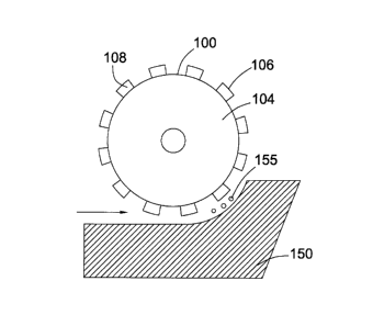
[0012] FIG. 1 is a schematic diagram showing an exemplary electrode
being
applied to machine a worpiece, in accordance with one embodiment of the
present
invention.
[0013] FIG. 2 is a perspective view of an exemplary electrode in
accordance
with one embodiment of the present invention.
[0014] FIG. 3 is a partially cut-away perspective view of the
electrode of FIG.
2, showing internal channels of a hub of the electrode.
[0015] FIG. 4 is a perspective view of an exemplary electrode in
accordance
with another embodiment of the present invention.
DETAILED DESCRIPTION
[0016] Embodiments of the present disclosure will be described
hereinbelow
with reference to the accompanying drawings. In the subsequent description,
well-
known functions or constructions are not described in detail to avoid
obscuring the
disclosure in unnecessary detail.
[0017] Approximating language, as used herein throughout the
specification
and claims, may be applied to modify any quantitative representation that
could
4
CA 3030524 2019-01-18
248371A
permissibly vary without resulting in a change in the basic function to which
it is
related. Accordingly, a value modified by a term or terms, such as "about" or
"substantially", is not to be limited to the precise value specified. In some
instances,
the approximating language may correspond to the precision of an instrument
for
measuring the value.
[0018] Any numerical values recited herein include all values from
the lower
value to the upper value in increments of one unit provided that there is a
separation
of at least 2 units between any lower value and any higher value. As an
example, if
it is stated that the amount of a component or a value of a process variable
such as,
for example, temperature, pressure, time and the like is, for example, from 1
to 90,
preferably from 20 to 80, more preferably from 30 to 70, it is intended that
values
such as 15 to 85, 22 to 68, 43 to 51, 30 to 32 etc. are expressly enumerated
in this
specification. For values which are less than one, one unit is considered to
be 0.0001,
0.001, 0.01 or 0.1 as appropriate. These are only examples of what is
specifically
intended and all possible combinations of numerical values between the lowest
value
and the highest value enumerated are to be considered to be expressly stated
in this
application in a similar manner.
[0019] Embodiments of the present invention take benefit by using
material
combinations achieved by unique fabrication methods to provide various
specific
electrodes for machining workpieces, for example, electrodes with both high
electrical conductivity and high thermal arc resistance, and possibly, with
built-in
flushing channels, and moreover, possibly in specially tailored geometries.
[0020] In one aspect, embodiments of the present invention provide a
specific
electrode. The electrode comprises a main body made from an additive material
fabrication process, which enables electrical conductivity and arc resistance
of the
main body to be tuned based on materials used, and also enables at least one
internal
flushing channel to be installed into the main body. The electrode also
comprises one
or more internal flushing channels used to introduce a flushing liquid to a
volume
between the electrode and a workpiece to be machined, to enhance evacuation of
the
waste material produced by machining.
CA 3030524 2019-01-18
248371A
[0021] In certain embodiments, the whole main body of the electrode
may be
made from a single material. Alternatively, in certain embodiments, different
portions
of the main body of the electrode may be made from different materials.
[0022] In one embodiment, the main body of the electrode comprises
at least
two portions made from different materials but integratedly formed together
through
an additive material fabrication process. For example, in an electrode 100 as
shown
in FIG. 1, a main body comprises a main portion 104, and a machining portion
106
designed to electrically interact with a workpiece 150 to be machined. The
machining
portion 106 is designed to act on the workpiece 150 and then is able to cut
chips 155
from the workpiece via electric energy. For the illustrated arrangement, the
machining
portion 106 comprises a plurality of machining elements 108 protruding beyond
an
outer surface of the main portion 104 and spaced away from each other. The
main
portion 104 and the machining portion 106 are made from different materials,
but are
integrally combined through an additive material fabrication process. In
certain
embodiments, the machining portion 106 may be either conductive or
nonconductive
and have desired thermal arc resistance and/or hardness. In one embodiment,
the main
portion 104 is made from a first electrically conductive material, and the
machining
portion 106 is made from a second electrically conductive material having a
melting
point higher than that of the first electrically conductive material. The
first and second
electrically conductive materials provide the electrode with a good electrical
conductivity, and the second electrically conductive material provides the
machining
portion with a good thermal arc resistance as well. In one embodiment, the
first
electrically conductive material comprises at least one of copper, nickel,
aluminum,
and iron. The second electrically conductive material may be refractory
material
having a melting point higher than about 1800 C. In one embodiment, the
refractory
material comprises at least one of tungsten, molybdenum, and chromium.
[0023] The internal flushing passage fabricated within the electrode
through
the additive material fabrication process endures high pressure and thereby
supplies
high pressure flushing to the volume between the electrode and the workpiece
to be
machined. The internal flushing passage may be complex in shape. In one
6
CA 3030524 2019-01-18
248371A
embodiment, the internal flushing passage comprises a curved channel built
within
the electrode.
[0024] In a certain embodiment, the additive material fabrication
process can
be defined as a process of joining materials to make one or more objects from
digital
data such as 3D CAD (Computer Aided Design) model data, usually layer upon
layer,
as opposed to subtractive manufacturing methods such as traditional machining.
An
additive material fabrication process is capable of directly manufacturing
finished
components based on just three inputs: a raw construction material or
materials (often
in the form of powder or wire for metals processes), energy for consolidation
of that
construction material (often a laser beam, electron beam, or arc source for
metals
processes, and a digital representation (CAD model) of the component. Examples
of
additive material fabrication processes include but are not limited to, powder-
bed
methods such as selective laser melting, direct metal laser sintering, and
electron-
beam melting, or 3-dimensional ink-jet printing as well as powder- or wire-fed
methods such as 3-dimensional cladding or laser forming.
[0025] Metal powder-bed additive manufacturing methods combine
precision
powder bed formation for material deposition with high-resolution laser- or
electron-
beam micro-welding for direct material consolidation of fine, uniformly sized
powders. For example, in a selective laser melting process, a uniformly thick
layer
of metal powder is first spread on a suitable metal substrate, and then a
laser beam is
scanned across the powder bed in a specified pattern so as to weld and attach
the first
layer in the part to the build substrate. The steps of powder spreading and
laser
micro-welding then are repeated layer after layer until the final layer is
consolidated
and the part is completed. Complex internal passages, cavities or lattice
macrostructures are readily created by leaving the loose powder material
unconsolidated in those regions for removal after the build is completed. In
contrast,
powder- or wire-fed 3-dimensional cladding processes are accomplished by
directing
a laser beam, electron beam, or arc source at a substrate to create a melt
pool while
adding powder or wire material into the melt pool. To create the desired
geometry,
the beam is scanned to carry the melt pool across the substrate while material
is
continuously added to the moving melt pool. For example, in a powder laser
forming
7
CA 3030524 2019-01-18
248371A
process, a laser beam heats the substrate to produce a melt pool that is
scanned across
the substrate and metal powder is sprayed from a powder delivery nozzle and
injected
into the moving melt pool to produce consolidated material. Once the initial
layer is
completely formed, these steps are repeated layer after layer until the final
layer is
consolidated and the part is completed.
[0026] FIG. 2 and FIG. 3 show an electrode 200 fabricated by an
additive
material fabrication process. The electrode 200 is configured in a wheel shape
and
comprises an elongated rotating shaft 204 and a hub 206 that can rotate with
the
rotating shaft 204. A plurality of blocks 208 protrude beyond a
circumferential outer
surface 210 of the hub 206 to function as machining elements, which form a
discontinuous circumferential outer surface 212 for facing and acting on the
workpiece to be machined to remove materials from the workpiece via electric
energy.
In the illustrated arrangement, due to the protruding blocks, the hub 206
therefore is
segmented into a plurality of spaced discharge sections 209 by the machining
elements 208 (see FIG. 3). The discharge sections 209 and the machining
elements
208 may be disposed alternately for performing the electro-machining. .
[0027] The additive material fabrication process enables the
rotating shaft 204,
the hub 206 and the blocks 208, which are integratedly formed together, to be
made
from same or different materials. In a certain embodiment, the whole electrode
200
is made from a same material. Alternatively, in a certain embodiment, at least
two of
the rotating shaft 204, the hub 206 and the blocks 208 are made from different
materials. For example, the blocks 208 may be made from one material while the
rest
of the electrode 200, i.e., a main portion of the electrode 200 including the
rotating
shaft 204 and the hub 206, is made from a different material. In one
embodiment, the
blocks 208 are made from an electrically conductive material (e.g., tungsten,
molybdenum or their alloys) having a melting point higher than that makes the
rest
of the electrode 200 (e.g., copper or its alloys).
[0028] FIG. 3 is a cross section view showing an internal structure
of the hub
206. As shown in FIG. 3, the electrode 200 comprises an internal flushing
channel
214 for introducing a flushing liquid to a volume between the electrode and a
8
CA 3030524 2019-01-18
248371A
workpiece to be machined. The flushing channel 214 is fabricated through an
additive
material fabrication process and therefore is capable of enduring high
pressure during
high pressure flushing. In the illustrated embodiment, the internal flushing
channel
214 connects entrances 216 on a circumferential outer surface 218 of the
rotating shaft
204, with a plurality of slots 220 defined between the blocks 208 and the
discharge
sections 209. The flushing channel 214 comprises a central hole (not shown)
extending within the rotating shaft 204 from the entrances 216 to a center
hollow
passage 224 of the hub 206, and a plurality of channels 226 connecting the
center
hollow passage 224 and the plurality of slots 220 where the flushing liquid
exits the
electrode, respectively.
[0029] Referring to FIG. 4, another electrode 300 made by an
additive
material fabrication process is provided. The electrode 300 is configured in a
wheel
shape and comprises an elongated rotating shaft 304 and a hub 306 that can
rotate
with the rotating shaft 304. An outer circumferential layer 308 of the hub 306
functions as a machining portion and provides a circumferential outer surface
310 for
facing and acting on the workpiece to machine material from the workpiece. The
additive material fabrication process allows various material combinations and
therefore different portions of the electrode can be be made from different
materials.
In one embodiment, the outer circumferential layer 308 is made from an
electrically
conductive material having a melting point that is higher than that of the
material used
to produce the rest of the electrode 300. In one embodiment, the outer
circumferential
layer 308 has a thickness ranging from 5 mm to 15 mm. In a specific
embodiment,
the outer circumferential layer 308 has a thickness approximately of 10 mm.
[0030] The electrode 300 further comprises a built-in internal
flushing
passage 314 for introducing a flushing liquid to a volume between the
electrode and
a workpiece to be machined. The flushing channel 314 is fabricated with an
additive
material fabrication process and therefore is capable of enduring high
pressure during
high pressure flushing. In the illustrated embodiment, the internal flushing
passage
314 connects entrances 316 on a circumferential outer surface 318 of the
rotating shaft
304, with at least one, or preferably, a plurality of exits 320 on the
circumferential
outer surface 310. The flushing passage 314 comprises a central hole (not
shown),
9
CA 3030524 2019-01-18
24837 IA
extending within the rotating shaft 304 from the entrances 316 to a center
hollow
passage 324 of the hub 306, and a plurality of curved channels 326 connecting
the
center hollow passage 324 and the plurality of exits 320 where the flushing
liquid
exits the electrode, respectively. The channels 326 are curved in a manner
that the
flushing liquid can be stably and uniformly delivered to the exits during
rotation of
the electrode 300. It should be noted that the built-in internal flushing
passage 314
inside the electrode 300 that is represented with dotted lines actually is
invisible, and
it is shown for the convenience of illustration only.
[0031] In use, current flows to the electrode to machine a
workpiece, while a
flushing liquid flows through internal passages in the electrode to a volume
between
the electrode and the workpiece, enabling the solid particles or debris
removed from
the workpiece to be carried away and the workpiece to be cooled.
[0032] In another aspect, a method for manufacturing an electrode
with an
additive manufacturing system is provided. The additive manufacturing system
used
herein refers to a system, such as a selective laser melting system or an
electron beam
melting system, wherein materials are added sequentially in a layer-by-layer
fashion
with the purpose of creating a component. In certain embodiments, the additive
manufacturing system comprises a powder delivery nozzle and a thermal source.
In
one embodiment, the additive manufacturing system comrpsies a laser forming
device. The method comprises: providing a digital representation, such as a
CAD
(Computer Aided Design) model, of an electrode with at least one built-in
internal
flushing passage for internal liquid flushing; creating a sequence or stack of
layers
based on the digital representation, applying manufacturing parameters to each
of
those layers based on the digital representation; and producing the physical
electrode
by sequentially adding and consolidating material for each layer on top of the
previous layer until the entire electrode is completed.
[0033] The processes of adding material and consolidating material
may be
executed in parallel, or in sequence, or a combination of both. For example,
in
powder-bed methods, the powder is spread on a substrate, and then consolidated
by
scanning across the powder bed using a laser beam. In certain embodiments, the
CA 3030524 2019-01-18
248371A
material is consilidated while the material is added to the build region. For
example,
in one embodiment, the powder delivery nozzle and the laser beam may be
coxially
installed to consolidate material while the material is added to the build
region.
[0034] In one embodiment, the associated manufacturing parameters
created
for each of the layers in the digital representation comprise parameters for
fabricating
at least one built-in internal flushing channel of the electrode. In one
embodiment, the
material is delivered and added under a gas. In one embodiment, the material
is added
in the form of powder having a particle size ranging from about 50 microns to
about
250 microns.
[0035] Producing an electrode with an additive manufacturing process
allows
practical fabrication of delicate and complex interior flushing channel
geometries
which are impossible to create by conventional metal processing methods such
as
machining, casting, or molding. Additive manufacturing of an electrode also
allows
novel material combinations in which material composition gradients may be
formed,
for example, by slowly changing the powder during the building process.
Material
composition gradients allow altering either the arc resistance or the
electrical
conductivity in different regions of the final electrode.
[0036] In certain embodiments, the use of an additive manufacturing
process
may comprise consolidating a first electrically conductive material in one or
more
layers, or regions of layers according to the digital representation of the
electrode
while consolidating a second electrically conductive material having a melting
point
higher than that of the first electrically conductive material in the
alternate layers or
regions of the layers according to the digital representation of the
electrode.
[0037] In one embodiment, powder of the first electrically conductive
material
is delivered additively to a build layer or region of a layer under a cover
gas while a
thermal source, such as a laser, is used to join the powder together. The
process is
repeated until a first portion of a desired shape is obtained. Then powder of
the
second electrically conductive material is delivered additively to alternate
layers or
regions of layers and joined together onto the first portion, and the process
is repeated
11
CA 3030524 2019-01-18
248371A
until a second portion of a desired shape is obtained. The delivery and
joining of the
first and second electrically conductive materials using an additive
manufacturing
process may be alternated and/or repeated until the final shape is obtained.
The final
shape may have a series of internal cavities and channels with complex
geometries
that are useful for internal liquid flushing.
[0038] While the
disclosure has been illustrated and described in typical
embodiments, it is not intended to be limited to the details shown, since
various
modifications and substitutions can be made without departing in any way from
the
scope of the present disclosure. As such, further modifications and
equivalents of the
disclosure herein disclosed may occur to persons skilled in the art using no
more than
routine experimentation, and all such modifications and equivalents are
believed to
be within the scope of the disclosure as defined by the subsequent claims.
12
CA 3030524 2019-01-18