Note: Descriptions are shown in the official language in which they were submitted.
CA 03031328 2019-01-18
WO 2018/022126
PCT/US2016/063838
SYSTEMS, APPARATUSES AND METHODS FOR DUAL LINE INBOUND
DETECTION ON A DATA COMMUNICATION 1.3.1J,S
BACKGROUND OF THE INVENTION
Field of the Invention:
100011 The present invention relates to systems, methods and apparatuses
for
apparatuses for dual line inbound detection on a data communication bus.
Description of Related Art:
[00021 Modern conveyors such as those employed in mining and manufacturing
operations can exceed 4 kilometers (km) in underground installations and 10
kin in overland
installations, General conveyor operational parameters are monitored along the
entire length
of the installation, these include: belt wander, belt tear, belt slip and
bearing temperatures, to
name a few. These parameters are often difficult to monitor given the
distances involved and
the lack of power. Further, in the operation of any conveyor installation,
.there is a need for
safety functions such as stopping the conveyor in an emergency situation, and
safely remote
isolating the conveyor for maintenance purposes, among other operations,
10003] In addition, conveyor installations are, by their nature, hostile
environments fbr
any electrical equipment and cabling that may be installed on their
superstructure. The
equipment and particularly the cabling is subject to vibration, dust, falling
material, rain,
extremes in temperature and exposure to radiation, all of which can result in
the introduction
of electrical faults that can. compromise the integrity and safety of these
monitoring systems
and require fast reaction times (e.g., for a controller to accomplish a basic
emergency stop
and isolation function at a. remotely monitored device deployed along the
conveyor).
[00041 SILBUS is an example of an existing input/output (I/O) and control
system
having a. data. communication bus deployed between a controller and field
devices along a
conveyor or other industrial system having equipment andlor monitored sensors
distributed
over or along a geographically large area or long distance for industrial
applications and often
CA 03031328 2019-01-18
WO 2018/022126
PCT/US2016/063838
- 2 -
in harsh environments. SILBUS is commercially available from Austdac Pty Ltd,
an affiliate
of Hubbell Incorporated, with offices in New South Wales and Queensland in the
Commonwealth of Australia and in Pittsburgh, Pennsylvania in the United States
of America.
SILBUS is a family of intrinsicall:,,,r safe (IS) fieldbus products designed
for use in hazardous
area underground mining or similar industrial applications. SILBUS provides
data
transmission and power on twisted pair wires for monitoring and control in
industrial systems
that are, fbr example, as many as 10 km in length, including a control unit or
channel
generator that is in communication with a range of distributed modules (i.e.,
input and output
devices) that monitor a range of signals such as digital, safety transmitters,
voltage, current,
temperature, and frequency.
[00051 The Austdac SILBUS method of conveyor monitoring and control uses a
one
cable approach to both monitoring and control of long distance conveyors with
long distance
transmission over 10 kin, for example. SILBUS employs a transmission method
which allows
for the combined transmission of safety-rated (e.g., SIL3 according to the
International
Standard IEC 61508 or its Australian edition, AS 61508) conveyor emergency
stop signals
with monitoring and control signals for field devices such as belt alignment
switches, tilt
switches, belt rip switches, as well as analog values relating to bearing
temperature and
vibration.
100061 in SILBUS, all safety and standard digital inputs are down. line
powered,
eliminating the need tbr external power along the length of conveyor. For
example, one field
device that is commonly deployed along a conveyor is a pull key, which is used
to provide
controlled stop fimctions fbr distributed plant conveyors. The Austdac pull
key or cable-pull
limit switch type ESS3 has many applications in controlling a distributed
plant such as
conveyors or belts used in mining or materials handling industries. The pull
key can be
operated using a front, centrally-located knob or each of two side-located,
flexible cable-pull
actuators. The side cable-pull actuators can be used in tensioned and non-
tensioned systems.
The control and monitoring transmitters in a pull key are system powered, such
that no
external power source needs to be connected along the length of the conveyor.
[00071 SILBUS, however, has limitations in terms of noise immunity (e.g.,
from
variable frequency drives), and limitations with respect to the number of
channels for input
CA 03031328 2019-01-18
WO 2018/022126
PCT/US2016/063838
- 3 -
and output devices, as well as limitations on transmission distances on large
overland
conveyors, and line powering of the distributed devices. For example, many
large motors are
used to power conveyors; these motors are switched on and off, change speed
from low to
high and trip off on overload. Variable speed motor drives are also employed.
Because these
activities all take place at the end of relatively long supply cables, the
electrical environment
is characterized by the presence of large switching transients, general
electrical noise and
harmonics,
[0008] A need therefore exists for a distributed I/O system that has
improved noise
immunity. Further, a need exists for an improved system and method of
detecting inbound
transmissions from field devices on a two-wire data communications bus in a
distributed I/O
system to accurately and reliably detect valid inbound transmissions, even in
the presence of
noise, while minimizing false detection of noise as an inbound transmission.
SUMMARY OF THE INVENTION
100091 The above and other problems are overcome, and additional
advantages are
realized, by illustrative embodiments of the present invention.
[0010] In accordance with illustrative embodiments of the present
invention, methods
and systems are provided to determine if a device has sent a valid inbound
transmission on a
bus that interfaces a control unit to plural devices connected to the bus. The
bus is a two wire
bus having a signal line and a common return line. The control unit is
configured to generate
a pulse train comprising: a plurality of cycles for transmission on the bus,
each of the cycles
comprising a low voltage level portion for a designated period of time and a
high voltage
level portion for a designated period of time, and at least some of the cycles
corresponding to
respective channel windows assigned to respective ones of the plural devices
as I/O channels;
and bus scan cycles that each comprise a selected number of the I/O channels,
and a
synchronization pulse. The synchronization pulse is configured to ensure that
the plural
devices transmit and receive on their corresponding I/O channels and that the
control unit
samples the pulse train at a correct channel window or pulse corresponding to
a selected one
of the plural devices. Each of the plural devices is configured to indicate an
inbound
CA 03031328 2019-01-18
WO 2018/022126
PCT/US2016/063838
- 4 -
transmission to the control unit by pulling down the signal line to a
designated low voltage
level during the low voltage level portion of its corresponding cycle. The
method comprises
operating a high side current detector to detect current on the signal line;
operating a low side
current detector to detect current on the common return line; designating a
signal threshold;
designating at least part of the low voltage level portion in each of the 110
channels to be that
channel's inbound detection period; determining an average for a designated
number of
samples of the current detected by the high side current detector during a
channel's inbound
detection period; determining an average for a designated number of samples of
the current
detected by the low side current detector during the channel's inbound
detection period; and
determining an inbound transmission to be valid if the average of the samples
from the low
side current detector and the average of the samples from the high side
current detector are
both greater than the signal threshold.
[00111 in accordance with another illustrative embodiment of the present
invention,
the method comprises: operating a high side current detector to detect current
on the signal
line; operating a low side current detector to detect current on the common
return line;
designating a high side signal threshold and a low side signal threshold;
designating at least
part of the low voltage level portion in each of the 1/0 channels to be that
channel's inbound
detection period; determining an average for a designated number of samples of
the current
detected by the high side current detector during a channel's inbound
detection period;
determining an average for a designated number of samples of the current
detected by the low
side current detector during the channel's inbound detection period; and
determining an
inbound transmission to be valid if one of averages comprising the average of
the samples
from the low side current detector and the average of the samples from the
high side current
detector is greater than the high side signal threshold and the other one of
the averages is
greater than the low side signal threshold.
[0012j In accordance with aspects of illustrative embodiments of the
present
invention, a signal on the bus is determined to not be a valid inbound
transmission when
outputs from either one of the low side current detector and the high side
current detector
fails to meet one of the high side signal threshold and the low side signal
threshold,
CA 03031328 2019-01-18
WO 2018/022126
PCT/US2016/063838
- 5 -
100131 in accordance with aspects of illustrative embodiments of the
present
invention, the low side current detector is disabled during the high voltage
pulse in the 110
channels,
[0014] In accordance with aspects of illustrative embodiments of the
present
invention, the pulse train is an offset square wave and the high voltage level
pulse is between
12 VDC and 48 VDC and the low voltage level portion is between 2 VDC and 9
VDC,
100151 In accordance with aspects of illustrative embodiments of the
present
invention, the pulse train is a periodic waveform comprising instantaneous
transition between
the high voltage level pulse and the low voltage level portion,
100161 In accordance with aspects of illustrative embodiments of the
present
invention, the pulse train has a configurable frequency.
[0017] In accordance with aspects of illustrative embodiments of the
present
invention, the bus scan cycles comprise dual scan bus cycles having
alternating A and B scan
cycles where each A scan cycle and each B scan cycle comprises the selected
number of I/0
channels and that synchronization pulse.
[0018] In accordance with aspects of illustrative embodiments of the
present
invention, the pulse train is an offset square wave with configurable
frequency, and
comprises a selected number of cycles that are assigned to a corresponding
number of the I/O
channels and that are generated by the control unit. For example, the selected
number of I/0
channels is configured in the control unit.
[0019] Illustrative embodiments and respective aspects thereof can be
used with other
illustrative embodiments.
[0020] Additional and/or other aspects and advantages of the present
invention will
be set forth in the description that follows, or will be apparent from the
description, or may be
learned by practice of the invention. The present invention may comprise an
ITO and control
system and data communication bus protocol and methods for forming and
operating same
having one or more of the above aspects, and/or one or more of the features
and combinations
thereof. The present invention may comprise one or more of the features and/or
combinations of the above aspects as recited, for example, in the attached
claims.
CA 03031328 2019-01-18
WO 2018/022126
PCT/US2016/063838
- 6 -
BRIEF DESCRIPTION OF THE DRAWINGS
10021] The present invention will be more readily understood with
reference to the
illustrative embodiments thereof as shown in the attached drawing figures, in
which:
100221 Fig, I is a block diagram of an input/output (i/O) and control
system
employing a data communication bus protocol in accordance with an embodiment
of the
present invention.
100231 Fig, 2 is a diagram illustrating bus signal voltage levels of an
example physical
layer of the I/O and control system in accordance with an embodiment of the
present
invention,
[0024] Fig. 3 is a block diagram of a control unit employed in the 1/0
and control
system in accordance with an embodiment of the present invention.
[0025] Fig. 4 is a block diagram of bus interface circuitry employed in
the control
unit of Fig. 3 and constructed in accordance with an embodiment of the present
invention,
[00261 Figs, 5A and 5B illustrate, respectively a perspective exterior
view and a block
diagram of an example field device in the Il0 and control system in accordance
with an
embodiment of the present invention such as a pull key housing in which a
transmitter is
deployed.
100271 Fig. 6A is a diagram of a pulse train employed in a data
communication bus
protocol in accordance with an embodiment of the present invention.
100281 Fig. 6B is a table providing scan cycle states and corresponding
values for the
pulse train of Fig. 6A,
[0029]
[0030] Figs, 7A and 7B are signal diagrams illustrating outbound channel
pulse
timing of a data communication bus protocol in accordance with an embodiment
of the
present invention.
100311 Figs, 8A and 8B are signal diagrams illustrating inbound channel.
pulse timing
of a data communication bus protocol in accordance with an embodiment of the
present
invention.
CA 03031328 2019-01-18
WO 2018/022126
PCT/US2016/063838
- 7 -
[0032] Figs. 9 and 10 are, respectively, a high side current sense
circuit and a low side
current sense circuit for use with a channel generator and constructed in
accordance with an
embodiment of the present invention,
[00331 Fig. 11 is a current sense amplifier circuit for use with a high
side current
sense circuit and a low side current sense circuit associated with a channel
generator and
constructed in accordance with an embodiment of the present invention.
100341 Fig. 12 are wavefolins illustrating an example of a data
communication bus
signal of the 1.10 and control system, and outputs from the high side current
sense circuit and
the low side current sense circuit, in the absence of noise interference.
10035] Fig. 13 are waveforms illustrating an example of a data
communication bus
signal of the and control system, and an output from the low and high side
current sense
circuits, during no transmission and in the presence of a transient pulse and
noise coupled to
the data communication bus which manifests on the low side current sense
signal.
100361 Fig. 14 are waveforms illustrating an example of a data
communication bus
signal of the 1./0 and control system, and an output from the low and high
side current sense
circuits, during no transmission and in the presence of a transient pulse and
nOise coupled to
the data communication bus which manifests on the high side current sense
signal.
[00371 Fig. 15 are waveforms illustrating an example of a data
communication bus
signal of the 110 and control system, and outputs from the high side current
sense circuit and
the low side current sense circuit, during transmission and in the presence of
noise coupled
to the data communication bus, and a single minimum level for valid
transmission detection
in accordance with an embodiment of the present invention.
[00381 Fig. 16 is similar to Fig. 15 except that upper and lower
detection levels for
valid transmission detection are used in accordance with an embodiment of the
present
invention.
100391 'Fig. 17 is a waveform illustrating an example of a data
communication bus
signal of the I/O and control system, and outputs from the high side current
sense circuit and
the low side current sense circuit, in the presence of pulse noise during
transmission, and.
upper and lower detection levels for valid transmission detection in
accordance with an
embodiment of the present invention,
CA 03031328 2019-01-18
WO 2018/022126
PCT/US2016/063838
- 8 -
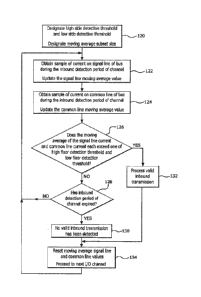
[0040] Fig. 18 is a flow chart illustrating operations to detect valid
transmissions on
the data communication bus in accordance with an embodiment of the present
invention.
[00411 Throughout the drawing figures, like reference numbers will be
understood to
refer to like elements, features and structures.
DETAILED DESCRIPTION OF ILLUSTRATIVE EMBODIMENTS
[0042] Reference will now be made in detail to embodiments of the present
invention,
which are illustrated in the accompanying drawings, The embodiments described
herein
exemplify, but do not limit, the present invention by referring to the
drawings. As will be
understood by one skilled in the art, terms such as up, down, bottom, and top
are relative, and
are employed to aid illustration, but are not limiting,
[00431 The following definitions are provided for reference in connection
with the
following description of various aspects of illustrative embodiments of the
present invention:
[0044] ADC: analog to digital converter,
[0045] channel pulse or window: a cycle comprising low voltage level
portion for a
designated period of time, and a high voltage level portion for a designated
period of time,
[00461 channel bandwidth: total time allocated to each channel pulse
(e,g, default
value of 2400us),
[00471 channel generator or control unit: a controller module that
generates an
outbound waveform and receives inbound transmissions,
[0048] common line: a low voltage (e.g., 0 V) return line,
100491 high floor (or high side) value or threshold: an upper current
level required for
valid inbound signal transmission,
100501 inbound: transmission from a line device to the channel generator,
100511 low floor (or low side) value or threshold: lower current level
required for
inbound signal transmission,
[00521 mark: inbound or outbound transmission within a channels window,
[00531 outbound: transmission from the channel generator to line device,
[0054] pulse pair: two pulses which represent the state of a channel,
CA 03031328 2019-01-18
WO 2018/022126
PCT/US2016/063838
- 9 -
[0055] receiver: a line device that listens for outbound messages,
[0056] signal line: a high side or voltage line with waveform generated
by the
channel generator,
[0057] space: inbound or outbound non-transmission within a channel's
window,
[0058] transmitter: a line device that transmits inbound messages.
[0059] With reference to FIG. 1, an I/O and control system 10 is provided
in
accordance with an illustrative embodiment of the present inventionõA.s
described below, the
I/O and control system 1.0 is advantageous because the channel generator
supports dual
current detection with respect to a two wire bus and a dual inbound detection
algorithm to
provide a significantly higher level of reliability in detection of inbound
transmission on the
bus and protection against false detection of inbound transmissions due to
noise, among other
reasons.
[0060] The .1/0 and control system 10 comprises Programmable Logic
Controller
(PLC) 14 and a display unit 16, which are shown connected to a control unit or
channel
generator 12. The PLC 14 and display unit 16 can be connected to the channel
generator 12
via Ethernet or RS485 MODBUSõ for example. The control unit or channel
generator 12 is
connected to a plurality of 1/0 modules via a bus indicated generally at 20.
The 1/0 modules
indicated generally at 22 can include, but are not limited to, one or more
pull-key transmitters
(I-IBTXPK), network monitor (HBMON), and other types of transmitters such as a
two
channel digital transmitter (H.13TX2D), an eight channel digital transmitter
(I-IBTX8D), a four
channel digital receiver (HBRX4D), and four channel analog receiver (I-
IBRX4.A), As shown,
one of the modules is operated as an end of line (EOL) monitor.
[0061] The illustrative II0 and control system 10 can be used for a
target industry
such as the overland conveyor industry and its associated activities such as
stacker reclaimers
and port coal loading facilities. The illustrative .110 and control system 10
can be used for
other industrial and commercial applications such as car parks (eg., having
parking space
sensors for parking space availability tracking), lighting automation, and
other systems which
employ monitoring by and control of many distributed input and/or output (i/O)
devices or
modules, The I/O modules are distributed or positioned at locations along a
conveyor, for
example, or other line or pattern depending on the system 10's industrial or
commercial
CA 03031328 2019-01-18
WO 2018/022126
PCT/US2016/063838
- 10 -
application, The I/0 modules are connected to each other and the controller or
channel
generator 12 by the bus 20.
[0062] The bus 20 can be, for example, any cable that allows
communication and
provides power over long distances. The bus can be a two wire system. For
example, the bus
can employ twisted pair for improved noise and crosstalk immunity as the cable
is a key area
for noise immunity. Addition& specifications for a cable deployed for the bus
20, for
example, can be 2,5mm2 cores, low capacitance, configured for reduced
reflection and
propagation delays, and no shield for ease of installation in normal
circumstances, but should
be provided for worst case scenario.
[006.3] The 1/0 and control system 10 can supply sufficient power to
supply line
powered I/0 modules or devices at a minimum 12.VDC from the controller 12, or
a supply of
48'VDC to allow for a required number of line powered devices depending on the
particular
application for which the system 10 is being used. For example, the supply of
a larger
voltage level (e.g., 48VDC) at the controller 12 can allow for better power
distribution on
long cable runs where there may be significant voltage drops on the line.
Channel bandwidth
can be selected and altered to supply sufficient power to 1/0 modules or
devices connected
via the bus and deployed along a conveyor or other line or pattern depending
on the system
10's industrial or commercial application.
[0064] Due to the longer conveyor or commercial or industrial lino
lengths needed, a
larger number of I/O modules or devices are also needed. The illustrative I/O
and control
system 10 can be configured, for example, to meet a minimum transmission
distance of 16
km. Further, the 110 and control system 10 can. be configured to operate a
minimum of 512
I/0 channels and to power a minimum of 320 transmitters from the bus 20, for
example,
which represents significant improvements and advantages over SILBUS and other
existing
110 and control systems. In addition, the 170 and control system 1.0 is
scalable, that is, it can
be configured to increase the number of channels with a decrease in refresh
rates and vice-
versa via the controller 12. Further, all of the 1/0 modules are automatically
self-configuring
for channel bandwidth and number of channels.
[0065] The physical layer of the I/0 and control. system 10 will now be
described
with reference to FIG. 2 and in accordance with an illustrative embodiment of
the present
CA 03031328 2019-01-18
WO 2018/022126
PCT/US2016/063838
- 11 -
invention, To maximize the distance covered by the system 10, the high voltage
level is
48VDC, for example. The voltage level at the low level shad be 5VDC, for
example.
Additionally, for example, no line devices (e.g., I/O modules) draw off the
line at 9VDC or
lower. When producing the low level supply voltage, the controller 12 passes
the voltage
through a current sensing circuit. Any devices that need to drive data in its
assigned channel
during the low voltage period can pull-down on the signal line to the common
line on the bus
20. Since there is no load on the low voltage level (5VDC), its output should
remain near
that level for the length of the line. The high level voltage side allows for
large voltage drops
in the bus signal and devices on the bus should remain operational down. to
12VDC. The use
of inbound current sensing devices in the channel generator 12 provides
significantly
increased levels of EMC protection over the voltage load and edge sensing
techniques used in
SILBUS. A minimum of 2A at 48VDC is generally available from the channel
generator or
controller 12.
100661 With reference to Figs. 3 and 4, an example of a dual port
controller or
channel generator 12 is provided which generates the bus signal, senses
incoming
transmissions from line devices 22 on the bus 20, and interfaces to the
outside world (e.g., via
.Ethernet or R.S485 interface). A 48VDC power source is connected to a power
supply 30
in the channel generator 12 that, in turn, provides operating voltages such as
12VDC for a
relay driver 28 and 3,3VDC for other electronic components such as a
microcontroller 36,
one or more bus interface circuits 34, and a communications interface 32. The
channel
generator 1.2 has channel logic decoding which in turn may be used to drive
relays for
controlling or signaling external devices. The channel generator 12 can have
LEDs (not
shown) for indicating health of the controller, power source and/or bus 20,
Ethernet activity,
and local digital input.
[00671 FIG. 4 is a block diagram of a channel generator bus interface 34
in
accordance with an illustrative embodiment of the present invention. High
(48V) and low
(5V) voltage protection and monitoring modules 40 and 42 provide conditioned
high and low
voltage signals to respective high and low voltage switches 44 and 46 to drive
the outbound
bus signal in accordance with a protocol as described in more detail below.
High side and low
CA 03031328 2019-01-18
WO 2018/022126
PCT/US2016/063838
12-
side current signals 48 and 50 carry incoming or inbound transmissions from
line devices on
the bus 20 that are detected via the current sense circuits 42 and 52.
[0068./ FiGs. 5A and 5B depict, respectively-, a pull-key transmitter
(IIBTXPKI) 22 as
an example I/O module or line device 22 constructed in accordance with an
illustrative
embodiment of the present invention. With reference to Fig. 5A, the two-input
transmitter
22 is fitted into a pull-key (or cable-pull limit switch) assembly. The pull
key is used to
provide controlled stop functions for distributed plant or conveyors. The pull
key can be
operated using the front centrally located knob 80 or each of the two side
located flexible
cable-pull actuators 82. The side cable-pull actuators 82 can be used in
tensioned and non-
tensioned systems.
[0069] With reference to Fig. 5B, the transmitter 22 has two inputs 62
driven by
voltage free contacts 60. One contact 60 is Normally Open (NO) and the other
contact 60 is
Normally Closed (NC). It is expected that the change-over of contacts occurs
at the same
time and only a single output channel is required. If both inputs are in the
same state, a fault
condition is considered to exist. The microcontroller 64 and bus interface 66
process the
inputs 62 for transmission on the bus 20. A power supply 68 receives power
(e.g., a low
voltage signal) from the bus to provide power to the components of the
transmitter 22. A
supervisory circuit 70 can be provided to monitory health of the transmitter
such as power
[00701 By way of another Il0 module or line device 22 example, a two
digital input
transmitter (IEBTX2D) is like the pull-key transmitter (HBTXPK). Transmitter
has two
inputs 62 driven by voltage free contacts 60. Rather than a single output with
dual input with
redundancy, the dual input transmitter outputs two separate states on
different channels. An
eight digital input transmitter (HBTX8D) has inputs driven by voltage free
contacts. States
output on 8 separate I/O channels on the bus 20. The eight-channel digital
transmitter is a
small line powered transmitter capable of transmitting the status of eight
voltage free contacts
and can be used for sensing the status of remote voltage free contacts such as
emergency
stop, pull key, belt wander, belt rip and blocked chute switches on long
conveyors to name
but a few. The transmitter can be line powered from the two-wire bus 20
network cable,
thereby reducing installation and cabling costs.
CA 03031328 2019-01-18
WO 2018/022126
PCT/US2016/063838
- 13 -
[00711 Additional examples of 110 modules 22 include, but are not limited
to, a four
channel analog transmitter (HBTX4A) with 0-2VDC or 0-20mA input, Any offsets
such as
0.4V or 4mA will not be removed but rather transmitted, Data (e.g., 12 bits +
4 CRC bits) is
transferred via the datalink protocol over the configured number of channels.
A four channel
analog receiver (HBRX4A) has 0-2VDC or 0-20niA output, Data (e.g., 12 bits + 4
CRC bits)
is transferred via the datalink protocol over the configured number of
channels.
[00721 Another example I/0 module 22 is a four channel receiver (HBRX4D)
with
digital (relay) outputs. The HBRX4D can receive from just a few through to
many digital
ON/OFF signals from the control system 10 bus network to control the four
relay outputs
directly or via complex multi-term logic functions. The digital receiver has
four output relays
controlled by up to six logic resolvers (4 physical linked to a relay and 2
virtual may be used
to drive a channel) capable of implementing OR, AND, NOR, 'NAND and FLIP logic
functions. Each resolver has an independently configurable output ON and OFF
delay filter
to allow implementation of simple timer functions. Further, a dual channel
temperature
transmitter (HBTX2T) has a temperature input designed to work with a standard
two, three or
four wire PT' 00 temperature sensor. The temperature transmitter can be
configured to
operate on one of two temperature ranges, -10 C to +100 C or -20 C, to +200 C,
which makes
the module particularly suited to monitoring bearing or similar plant
temperatures via the bus
20 network without any requirements for additional power. A network monitor
reports back
to the channel generator and control unit 12 various network and line
parameters such as, but
not limited to, line voltage, slew rate, reflection, and ground leakage. The
monitor
(HB.MON) may also be used to isolate downstream parts of the network to help
with fault
isolation.
[00731 The applications of the I/0 modules (e.g., transmitters and
receivers) are not
limited to conveyor installations, but can be used in any application where
the status of a
remote switch contact or relay contact is required to he monitored, for
example,
[00741 The data layer of the DO and control system 10 will now be
described in
accordance with an illustrative embodiment of the present invention. The basis
of data
transmission along the bus 20 is pulse width modulation (PWM) for outbound
communications (e.g., from control unit 12 to line devices such as the pull
key transmitter
CA 03031328 2019-01-18
WO 2018/022126
PCT/US2016/063838
- 14 -
(HBTXPK)) and current detection for inbound communications (e,g., from line
devices or
I/O modules to the control unit or channel generator 12). The channel
generator continuously
maintains an offset square wave of a configurable frequency, wherein each of
plural channel
windows or pulses comprises a low voltage portion and a high voltage portion.
A channel.
window or pulse can be used to represent one I/O channel described below.
Alternatively, a
designated plural number (e.g,, 2 or more) of channel windows or pulses can be
used to
represent one I/O channel. The number of channel windows and therefore the
number of
channels can be configured in the channel generator. The typical number of
channels is 64,
128, 256 or 512 (with 1024 and 2048 available for large systems),
[00751 The .i/0 and control system 10 is a distributed I/O system such
that not all
communications are from the field devices 22 to the control unit 12 or vice
versa. For
example, communications can be from field device 22 to field device 22. The
I/O and control
system 10 couples the inbound to the outbound communications, allowing
multiple receivers
(e.g., among the field devices 22 and control unit 12) to sample or eavesdrop
on a single
transmitter device, thus providing true distributed I/0. Coupling is achieved
upon the
channel generator sampling the inbound current detection and immediately
altering the
outbound pulse width modulation to reflect the state of the inbound channel.
In some
applications, the inbound and outbound communication can be un-coupled and is
referred to
split 1/0,
[00761 Example inbound and outbound channels in a pulse train on the bus
20 will
now be described with reference to Figs. GA, 6B, 7A, 713, 8A and 813. Fig, 6A
depicts a
complete scan of the bus 20 which consists of, for example, two complete
cycles of a pulse
train (hereinafter referred to as cycle A and cycle B). A pulse train can
comprise, for
example:
e A synchronization pulse (hereinafter sync pulse);
e Eight (8) control channels; and
fg 64 x n I/0 channels were n = L.32 (i.e. 64 to 2048 I/0
Channels). As will
be described below in connection with Figs. 6A and 613, each I/O channel
toggles its inbound and outbound state on alternating cycles, allowing for
CA 03031328 2019-01-18
WO 2018/022126
PCT/US2016/063838
- 15 -
unit detection (and removal detection) and providing improved noise
immunity of false triggers,
10077] By way of an example, the control channels can comprise 8 system
control
bits (e,g., Bits 1 through 8) wherein Bit I is a cycle sync indicator that is
set to indicate
whether the current pulse train is an A scan cycle or a B scan cycle. One or
more designated
system control bits can be unassigned to allow for future system configuration
or control
settings. For example, Bits 4 and 7 can be spare bits that can be assigned a
system control
function at a later date. The outgoing bits for Bits 4 and 7 are set as spaces
for all cycles. The
inbound bits for Bits 4 and 7 are not set by any line module 22. A Bit 5 can
be designated as
an emergency interrupt mode enabled indicator. In other words, if this bit is
set by the
channel generator 12, then a special priority interrupt mode is enabled for
transmitters to
indicate an emergency situation. If the priority interrupt feature is enabled,
then Bit 5 is set in
both of the A and B scan cycles. Bit 6 is a force multilink mode indicator for
system
diagnostic purposes, for example. Information can be requested from specific
registers in this
mode such as, for example, device 22 type, serial number, device status, and
so on. If Bit 6 is
set, then any safety functions automatically go to the safe state. Bit 6 can
be used to force
channels I to 16 to a multilink mode for all devices 22 programmed on these
addresses such
that these devices 22 will not transmit unless specifically addressed in a
multilink protocol, as
will any other device 22 addressed by the multilink protocol. Bits 2 and 3 can
be a digital
transmission sync bits that mark the beginning of, for example, a 12 bit data
+ 4 bit CRC
digital transmission where Bit 2 indicates a 2 bit per cycle transmission, Bit
3 indicates an 8
bits per cycle transmission and the combination of both Bits 2 and 3 indicate
the transmission
of 16 bits per cycle and are thus set as a mark state on the 8th, 2fid or
every pulse train cycle
respectively:. Bit 8 can be a fault bit such that, in the event of a system
fault being detected
by the channel generator /2, the outgoing fault bit is set as a mark to
indicate the fault
condition to the rest of the system 10. Likewise, if a major system fault is
detected by one of
the modules 22 (e.g., such as a failure of a safety function), the incoming
fault bit is set as a
mark and the channel generator 12 in turn sets the outgoing bit. Each
individual /10 module
can also indicate a failed state by driving both cycles of the scan with a
mark on the incoming
CA 03031328 2019-01-18
WO 2018/022126
PCT/US2016/063838
- 16 -
channel. It is understood that different types of, and more or less number of,
control channels
or control bits can. be used in a pulse train scan cycle A or B.
100781 Figs. 7A and 7B depict illustrative outbound pulse timing. For
example, at the
start of a channel, the signal drops from the high voltage level to the low
voltage level. A
'space' is 800ps (e,g., or 1/3 of the channel bandwidth) of low voltage level
before returning
to the high voltage level for the remaining time of the channel's bandwidth of
1600tts, A
'mark' is 1200us (e.gõ or 1/2 of the channel bandwidth) of low voltage level
before returning
to the high voltage level for the remaining time of the channel's bandwidth of
1200us (e.g.,
or 1/2 of the channel bandwidth again),
[0079] Figs, 8A and 8B depict illustrative inbound pulse timing. A
transmitter (e.g,
in a device 22) which has detected its channel in a pulse train cycle can.
either pull-down on
the bus 20 or it can be passive. The pull down is made during the first 50011s
and is detected
by the channel generator 12 via current measurement. For normal channels,
once a valid
pull down has been detected, the channel generator 12 will delay the rising
edge of the
channel pulse by an additional 400us (e.g., or 1/6 of the pulse bandwidth), It
is this dditional
delay to the rising edge of the pulse that other appropriately coded receivers
(e.gõ in devices
22) detect and act upon. Because the pulse train and modulation is present
along the entire
length of the bus 20, receivers may be placed at any convenient point along
the bus to
monitor a channel for local output. In fact, many receivers may monitor the
same channel or
transmitter,
100801 With reference to Fig. 6A and the table in Fig. 6B, each I/O
channel toggles its
inbound and outbound pulse-pair state on alternating cycles, allowing for unit
detection (and
removal detection), detection of stuck transmitters and providing improved
noise immunity of
false triggers. For example, each pulse train's I/O Channels pulse-pair carry
I bit of inbound
and outbound data. If an inbound pulse is set, then the channel generator 12
sets the outbound
state for that pulse. The channel generator may also set the outbound state
independent of the
inbound state. In normal operation, the channel states in the A-pulse train or
A-cycle and in
the B-pulse train or B-cycle are inverted states, In other words, if the
inbound and outbound
state of channel 2 is "ON" in the A-pulse train with a space-mark pulse pair,
then it has a
mark-space pulse-pair in the B-pulse train, Likewise, if the inbound and
outbound state of
CA 03031328 2019-01-18
WO 2018/022126
PCT/US2016/063838
channel 3 is "OFF" in the A-pulse train with a mark-space pulse pair then it
has a space-mark
pulse-pair in the B-pulse train. The exceptions to this are (1) a transmitter
missing or having
failed and then the channel pulse-pair in both pulse trains is a 'space'; (2)
a transmitter
indicating fault condition and then the channel pulse-pair in both pulse
trains is a 'mark'; and
(3) channels carrying data which transmit 2-bits of data (of a 12 bit value
plus 4 bit CRC)
consecutively each pulse train cycle.
[0081.1
With continued reference to Fig, 6A, a complete scan of the bus 20 consists of
two complete cycles of the pulse train (e.g,, cycle A and cycle B). For
illustrative purposes in
.Fig. 6A, channel 3 is shown transmitting an 'OFF' state, channel 2 is shown
transmitting an
'ON' state, channel 4 is transmitting a fault state and there are no other
devices present on
other channels. Pulse train A has:
* a sync pulse;
= 8 control channels (1st control channel is a 'mark' to indicate cycle A);
and
= a number of I/O channels which each consist of a pair of pulses.
O Channel 3 is transmitting an 'OFF' state so it has a mark-space pulse-
pair
in the A cycle.
* Channel 2 is transmitting an 'ON' state so it has a space-mark pulse-pair
in
the A cycle.
* Channel 4 is transmitting a FAULT state so it has a mark-mark pulse-pair
in the A cycle.
* All other channels have transmitters off,
Pulse train B has:
* a sync pulse;,
O 8 control channels (1.st control channel is a 'space' to indicate cycle
B);
and
O a number of I/O channels which each consist of a pair of pulses.
* Channel 3 is transmitting an 'OFF' state so it has a space-mark pulse-
pair
in the B cycle.
CA 03031328 2019-01-18
WO 2018/022126
PCT/US2016/063838
- 18 -
a Channel 2 is transmitting an 'ON state so it has a mark-space
pulse-pair
in the B cycle,
0 Channel 4 is .transmitting a FAULT state so it has a mark-mark
pulse-pair
in the B cycle.
0 All other channels have transmitters off.
Accordingly, with reference to Fig. 6A and the table in Fig. 6B, each I/0
channel toggles its
inbound and outbound pulse-pair state on alternating cycles, allowing for unit
detection (and
removal detection), detection of stuck transmitters and providing improved
noise immunity of
false triggers
100821 The channel generator 12 emits 8 control channels followed by the
configured
number of I11.) channels regardless of whether or not the channels have been
assigned to an
1/0 device, At the end of the control and channel pulses, the channel
generator 12 sends an
extended (e.g,, extra-wide) pulse that resets all of the counters in the field
devices 22 back to
zero before the pulse train is repeated. The long synchronization pulse is
used to ensure that
all field devices are kept in synchronization, ensuring that transmitters
transmit on the correct
Channel and receivers sample the pulse train at the correct time. Field
devices 22 can simply
count the pulses or channels until the count matches their assigned address
before
transmitting or receiving.
[0083] As stated above, most distributed 1/0 systems use either voltage
level or
current detection to determine if a remote device is attempting to transmit to
the control unit.
Although the current detection method is more robust than voltage level
detection, it is still
susceptible to noise from sources that may induce current on the line,
resulting in false
positives (e.g., inbound detection when there is no transmission) or false
negatives (e.g.,
inbound transmission that is not detected by the control unit receiver).
100841 in accordance with an illustrative embodiment of the present
invention, the
system 10 uses the current detection method to detect incoming transmissions
to the channel.
generator 12. In addition, the system 10 monitors both the common line and the
signal line of
the bus 20 in the two-wire distributed network and is therefore advantageous
over a
distributed I/O system wherein only one line of a two-wire bus is monitored.
Further, in
accordance with another aspect of an illustrative embodiment of the present
invention, a dual
CA 03031328 2019-01-18
WO 2018/022126
PCT/US2016/063838
- 19 -
line inbound detection algorithm is provided which has been derived from
system 10 testing
that compares the outputs of two current detection circuits 84 and 86
described below, and is
able to use these outputs and one or more designated thresholds to
differentiate between noise
and a valid incoming transmission from a field device 22 to the Channel
generator 12. The
combination of dual line inbound current detection circuitry with the dual
line inbound
detection algorithm provides a significantly higher level of reliability in
detection of inbound
transmissions and protection against false detection of an inbound
transmission due to noise,
[0085/ Dual Line Inbound Detection Circuitry
100861 As stated above, the system 10 can employ a pulse width modulated
(PWM)
waveform where each cycle or channel window has a low voltage level portion
and a high
voltage pulse as shown for example in Figs. 8A and 813. When the system 10 is
driven to the
low voltage level (e.g,, from 48V to 5V such as during the 12001as of low
voltage level of a
mark in a channel of 2400)ts, or at least during the first 500us of a channel
window with a
space during which a pull d.own could be made to indicate a mark), the current
drawn is used
to determine the state of the devices in the system. This current is sensed in
two separate
circuits such as the voltage protection (5V) and monitoring module 42 and the
current sense
circuit 52 shown in Fig. 4. Illustrative embodiments for implementing current
sense circuits
84 and 86 in the voltage protection (5V) and monitoring module 42 and the
current sense
circuit 52, respectively, are shown in Figs, 9 and 10.With reference .to Fig.
9, an illustrative
high side current detector 84 uses a current sensor 88 (e.g,, a Texas
Instruments INA169
integrated circuit) with a very low value sense resistor 90. The voltage
output is low level
(10-15mV) and is fed into the amplifier circuit 102.
[008 .71 With reference to Fig. 10, an illustrative low side current
detector 86 is
configured to measure the cable 20 return current. Such measurement is only
relevant when
the bus signal is at the low voltage level, since that is when the
measurements are made.
Accordingly, a MOSFET 96 is provided to short circuit the sense resistor 100
when the bus
signal is at the high voltage level.
100881 With reference to Fig, 11, both current detectors 84 and 86 have
voltage
outputs in the 10-15mV range. In order for these outputs to be processed by
the
CA 03031328 2019-01-18
WO 2018/022126
PCT/US2016/063838
- 20 -
microcontroller 36, they are amplified by an op-amp circuit 102, A dual op-amp
is used (e.g,
'National Semiconductor LMC6482AIM) with identical circuits for high and low
side
amplification. The amplifiers output a signal in the l-3V range for processing
by the
microcontroller 36. The high side current detector signal is fed into the gate
of a P-Charinel
MOSFET for limiting the current output of the low voltage supply.
[00891 Dual Line Inbound Detection Algorithm
[00901 To provide the algorithm empla.)yed by the microcontroller 36 to
monitor the
outputs from the current detectors 84 and 86, a significant amount of system
testing was
performed for modelling purposes using signal generators with various coupling
techniques
and generation of transient noise pukes by switching of electrical loads in
adjacent pairs of
wires in the signal cable. The system testing facilitated designation of a
high side threshold
or detection floor and a low side threshold or detection floor and the
efficacy of using both,
although a single threshold with high and low side current detection can also
work but not
likely as reliably.
100911 The efficacy of using high and low side detection floors or
thresholds versus
using a single threshold will now be illustrated in connection with .the
waveforms in Figs. 12-
17, Fig, 12 is an example waveform capture of the bus signal (104) and the
inbound high
side current detector output (108) and the low side current detector output
(106) with no noise
interference. As may be seen in this example idea/ situation, a single signal
level threshold
112 would be sufficient to determine the inbound status,
[00921 With reference to Figs. 13 and 14, it has been determined from the
afore-
mentioned testing and modelling that coupled noise and transient pulses
generally tend to
interfere with either the low side (common line) or high side (bus signal)
inbound current
detection but rarely both. Transient noise, in particular, may generate a
pulse that is generally
short in duration (e,g., <300p,$) and unlikely to cause a false positive
(false mark). A pulse
with current in the opposite direction to the inbound current may bring one
side (i.e,, line)
low, resulting in a false negative (e,g,, a false space) or, in other words, a
failure to detect an
incoming pulse. Likewise, coupled noise can generate a negative current
resulting in a false
CA 03031328 2019-01-18
WO 2018/022126
PCT/US2016/063838
- 21 -
negative but only induce a current on a single line during a non-transmitting
space which
would not be picked up as a transmission.
100931 Figs. 12-17 show the effects of a transient pulse on the low side
and high side
followed by noise coupled to the line from the signal generator. In the Figs.
12-17, the
horizontal cursor line (112) represents an illustrative single detection
threshold, Figs. 13 and
14 illustrate, respectively, a low side current detector pulse and a high side
current detector
pulse during no transmission. The single detection threshold 112 suffices in
Figs. 13 and 14
since these signals 106 and 108 are not difficult to differentiate. By
contrast, however, a
single minimum floor level is insufficient to differentiate between valid
incoming
transmissions and signals affected by noise, as illustrated in Fig. 15.
Setting the floor high to
overcome noise on the line during non-transmission, however, can cause valid
transmissions
to be missed if they are affected by noise. Conversely, setting the level too
low can result in
a signal affected by noise as being considered a valid transmission.
[0094] In accordance with an illustrative embodiment of the present
invention, upper
and lower detection floors or thresholds 114 and 116 are designated, as shown
in Fig. 16, As
determined via the afore-mentioned testing and modelling, generally coupled
noise and
transient pulses affect one side more than the other. Accordingly, for an
inbound signal to be
considered valid, then one side should meet an upper (higher) floor level, and
the other line
may have a reduced floor level which it must meet. These levels are
configurable via
parameter settings in the channel generator 12. A typical or default value for
the upper
threshold would be 85% (e.g., percentage of the maximum measurable value at
the ADC of
the microcontroller 36) and 60% for the lower threshold. Additionally, the
number of samples
for the moving average described below is set to ten samples for default
configurations, for
example. Using designated high side and low side detection thresholds or
floors eliminates
valid inbound transmission being disregarded as noise. Further, invalid
signals due to noise
are reliably disregarded since as they do not meet both floor levels 114 and
116
simultaneously. Fig. 16 is the same as Fig. 15 but also shows the upper and
lower floor levels
114 and 116 Which result in correct detection of an inbound transmission.
100951 It
was determined from the afore-mentioned testing and modelling that it is not
optimal to require all samples to be above the minimum floor values 114 and
116 for a set
CA 03031328 2019-01-18
WO 2018/022126
PCT/US2016/063838
- 22 -
number of samples. This is because, if any one sample was below the floor 114
or 1.1.6, the
requisite sample count would be reset and restarted. The requisite sample
count can be a
configurable parameter setting in the channel generator 12. Testing also
determined that noise
could cause a momentary dip below the floor level 114 or 116, which would then
make
meeting the minimum requisite number of samples more difficult for a positive
incoming
message. For example, Fig. 17 illustrates how the low current detect signal
(106) may drop
below even the low side floor level 116 momentarily during signal sampling. In
this case, the
microcontroller 36 in the channel generator 12 (e.g., a MSP430 microprocessor)
is sampling
both signal lines at a rate of approximately 12.5us. The transitions (e.g.,
high to low, and low
to high) on the trace (110) indicate the sampling windows, As illustrated in
Fig. 17, if all
samples of the low side current detector trace (e.g., 106) had to be above the
lower detection
floor 116, the inbound transmission would have been discarded. Accordingly,
the dual line
inbound detection algorithm can include averaging the current samples to
reduce the impact
of spurious ADC readings and eliminate the need to restart the minimum
requisite samples
count, which in turn reduces the probability of valid inbound transmissions
being discarded.
For the case of the low side current detector trace (e.g,, 106) in Fig,. 17,
the average of the
samples would have been above the lower floor and the transmission considered
valid.
[00961 The dual line inbound detection algorithm will now be described
with
reference to the illustrative embodiment in Fig. 18. For example, the
microcontroller 36 in
the channel generator 12 can be programmed to execute the algorithm whereby a
high side
detection threshold and a low side detection threshold are designated such as
dynamically
configured or preconfigured, as shown in block 120. For example, the channel
generator 12
can. be configured to dynamically set the threshold and number of samples for
the moving
average. By monitoring the inbound current of channels known to be
transmitting an
inbound signal, a high threshold may be determined over a period of time.
Likewise, by
monitoring the inbound current of channels known not to be transmitting, then
a low
threshold may be determined which is above the level of any noise on the
signal line. The
microcontroller 36 can then be provided with samples of the outputs from the
current
detection circuits 84 and 64, for example, as shown in blocks 122 and 124. As
described
above, the samples can be averaged.
CA 03031328 2019-01-18
WO 2018/022126
PCT/US2016/063838
- 23 -
[0097] in accordance with an embodiment of the dual line inbound detection
algorithm, the current detected on the signal line and the common line by the
detectors 84 and
86 is compared with the designated high side detection threshold and low side
detection
threshold (e.g., thresholds 114 and 116 in Figs, 16 and 17). As long as the
current detected
on the signal line exceeds one of the high side detection threshold and low
side detection
threshold and the current detected on the common line exceeds the other one of
the high side
detection threshold and low side detection threshold per block 126, a valid
inbound
transmission is detected (block 132); otherwise, no valid inbound transmission
is detected
once the inbound detection period of the channel has expired (blocks 128 and
130). The
moving average signal line value and moving average common line value are then
reset, and
the microcontroller 36 proceeds to process the next I/O channel (block 134),
[00981 As stated above, the microcontroller 36 in the channel generator 12
operates in
accordance with the dual line inbound detection algorithm to determine the
state of the field
devices 22 in the system 10 by using current drawn when. the system bus 20 is
driven to the
low voltage level (e.g., the low voltage level portion that precedes the high
voltage pulse in
the channel window of a field device's designated -110 channel). Once a
determination is
made as described with reference to block 126 in Fig. 18, the microcontroller
36 proceeds to
the next 110 channel in the pulse train on the bus 20 to look for a valid
inbound transmission
from the corresponding field device 22. Further, the algorithm can control the
microcontroller 36 to disable the low side current detector 86 (e.g., via the
MOSFET 96)
when the bus signal is at the high voltage level, as described above,
[0099/ The dual line inbound detection algorithm has been described as
implemented,
for example, via a microcontroller 36 in the channel generator 12. It is to be
understood that
some or all of the detectors 86 and 84, amplifier 102 and a processing device
programmed to
implement the dual line inbound detection algorithm can be incorporated into
one or more of
the components of the channel generator 12 or can be implemented in one or
more
components that are external to channel generator 12.
[00100] Additional embodiments and implementations
CA 03031328 2019-01-18
WO 2018/022126
PCT/US2016/063838
- 24 -
[001011 Illustrative embodiments of the present invention have been
described with
reference to operations at a programmable device such as a channel generator
12 or 1/0
module or device 22, or a separate processing device for using high side and
low side current
detector outputs and a dual line inbound detection algorithm. It is to be
understood, however,
that the present invention can also be embodied as computer-readable codes on
a computer-
readable recording medium. The computer-readable recording medium is any data
storage
device that can store data which can thereafter be read by a computer system.
Examples of
the computer-readable recording medium include, but are not limited to, read-
only memory
(ROM), random-access memory (RAM), CD-ROMs, DI/Ds, magnetic tapes, floppy
disks,
optical data storage devices. It is envisioned that aspects of the present
invention can be
embodied as carrier waves (such as data transmission through the Internet via
wired, or
wireless transmission paths). The computer-readable recording medium can also
be
distributed over network-coupled computer systems so that the computer-
readable code is
stored and executed in a distributed fashion.
1001021 The components of the illustrative devices, systems and methods
employed in
accordance with the illustrated embodiments of the present invention can be
implemented, at
least in part, in digital electronic circuitry, analog electronic circuitry,
or in computer
hardware, firmware, software, or in combinations of them. These components can
be
implemented, for example, as a computer program product such as a computer
program,
program code or computer instructions tangibly embodied in an information
carrier, or in a
machine-readable storage device, for execution by, or to control the operation
of, data.
processing apparatus such as a programmable processor, a computer, or multiple
computers.
A computer program can be written in any form of programming language,
including
compiled or interpreted languages, and it can be deployed in any form,
including as a stand-
alone program or as a module, component, subroutine, or other unit suitable
for use in a
computing environment. A computer program can. be deployed to be executed on
one
computer or on multiple computers at one site or distributed across multiple
sites and
interconnected by a communication network. Also, functional programs, codes,
and code
segments for accomplishing the present invention can be easily construed as
within the scope
of the invention by programmers skilled in the art to which the present
invention pertains.
CA 03031328 2019-01-18
WO 2018/022126
PCT/US2016/063838
-25 -
Method steps associated with the illustrative embodiments of the present
invention can be
performed by one or more programmable processors executing a computer program,
code or
instructions to perform functions (e.g., by operating on input data and/or
generating an
output). Method steps can also be performed by, and apparatus of the invention
can be
implemented as, special purpose logic circuitry, e.g., an FPGA (field
programmable gate
array) or an ASIC (application-specific integrated circuit).
[00103) Processors suitable for the execution of a computer program
include, by way
of example, both general and special purpose microprocessors, and any one or
more
processors of any kind of digital computer. Generally, a processor will
receive instructions
and data from a read-only memory or a random access memory or both. The
essential
elements of a computer are a processor for executing instructions and one or
more memory
devices fur storing instructions and data. Generally, a computer will also
include, or be
operatively coupled to receive data from or transfer data to, or both, one or
more mass storage
devices for storing data, e.g,, magnetic, magneto-optical disks, or optical
disks, .Information
carriers suitable for embodying computer program instructions and data include
all forms of
non-volatile memory, including by way of example, semiconductor memory
devices, e.g.,
EPROM, EEPROM,, and flash memory devices; magnetic disks, e.g., internal hard
disks or
removable disks; magneto-optical disks; and CD-ROM and DVD-ROM disks, The
processor
and the memory can be supplemented by, or incorporated in special purpose
logic circuitry.
NO1041 The above-presented description and figures are intended by way of
example
only and are not intended to limit the present invention in any way except as
set forth in the
f011ovving claims. It is particularly noted that persons skilled in the art
can readily combine
the various technical aspects of the various elements of the various
illustrative embodiments
that have been described above in numerous other ways, all of which are
considered to be
within the scope of the invention.