Note: Descriptions are shown in the official language in which they were submitted.
CA 03031862 2019-01-24
W02018/050473 PCT/EP2017/072113
1
Method for the Production of Electronic Components by Means of 3D Printing
The present invention concerns a method for the production of electronic
components
and/or porous components, particularly anodes, from valve metal powder by
means of
3D printing and the use of a valve metal powder for the production of
electronic
components and/or porous components by means of 3D printing. The present
invention
further concerns an anode that is obtainable by the method according the
invention and
an electrical component, particularly a capacitor, that comprises the anode
according to
the invention.
The increasing miniaturization of devices in information and communication
electronics
requires electronic components with higher levels of performance and more
compact
design. This particularly concerns capacitors that are used as passive
elements for storage
of electrical energy in electronic components such as smartphones, laptops,
tablets,
wearables and the like. There is thus a need for capacitors characterized not
only by high
energy storage density, but also by smaller overall size, particularly low
thickness.
As a rule, valve metals used to produce capacitors are characterized in that
their oxides
allow current to flow through in one direction when potential is increased,
but to block
the current flow in the other direction when it is decreased. A further
property of valve
metals is that they have a natural oxide layer that prevents further oxidation
and thus
spontaneous ignition of the metal.
Anodes composed of valve metals are ordinarily produced by pressing and
sintering of
suitable metal powders having fine-particulate primary structures or already
having
sponge-like secondary structures. Solidification usually takes place by means
of solid-
phase sintering at temperatures in the range of 1000 C to 1500 C. In order to
allow
electrical contacting of the pressed bodies, the powder is pressed around a
connecting
wire. In this case, the minimum thickness of the anode is significantly
limited by the
diameter of the connecting wire. A problem in this production method is
absorption of
oxygen during the production process, which has a particularly negative effect
on the
hardness and/or ductility of the resulting anode. It has been found that a
higher oxygen
content in anodes leads to sharply impaired electrical properties of the
resulting
capacitor.
CA 03031862 2019-01-24
W02018/050473 PCT/EP2017/072113
=
2
In order to deal with this problem, methods were developed by means of which
the
oxygen content in anodes can be lowered by means of reducing conditions.
For example, US 4,722,756 describes a method for reducing the oxygen content
of
tantalum or niobium sintered bodies in which sintering is carried out in a
hydrogen
atmosphere in the presence of a reducing material. Proposed examples of the
reducing
material are beryllium, calcium, cerium, hafnium, lanthanum, lithium,
praseodymium,
scandium, thorium, titanium, uranium, vanadium, yttrium and zirconium, as well
as
mixtures and alloys thereof.
DE 3309891 describes a two-stage method for the production of sintered valve
metal
anodes in which already-sintered tantalum bodies are deoxidized in the
presence of a
reducing metal such as magnesium. For this purpose, the metal is introduced
into a
reaction chamber together with the sintered body and simultaneously heated
with said
body to temperatures between 650 C and 1150 C.
However, the methods described above have the drawback that treatment impairs
the
bonding of the connecting wire to the anode. However, the strength with which
the wire
and the anode are connected to each other, the so-called wire pull strength,
is an
important characteristic value, and insufficient bonding or low wire pull
strength
constitute a significant weakness in further processing of the capacitor,
which can lead to
mechanical failure of the capacitor.
An alternative method for the production of capacitors is printing of anodes
composed of
valve metals by application of metal-containing pastes to substrates. By
applying thin
layers to e.g. tantalum films, it is possible to obtain anodes that in some
cases have a
much lower thickness than that of conventionally produced components.
DE 102011116939 describes a method for the production of distortion-free
anodes by
means of screen or stencil printing on thin tantalum or niobium foils. The
anodes
produced by this method have a vertical dimension of 25 to 250
The pastes used are ordinarily systems comprising a plurality of components,
such as
metals, binders, solvents and optionally further additives. However, in order
to prevent a
negative effect on the electrical properties of the anode, these additives
must be
removed after printing. This is usually carried out thermally, which requires
an additional
CA 03031862 2019-01-24
W02018/050473 PCT/EP2017/072113
3
method step. Depending on the binders and/or solvents used, thermal treatment
may
cause them to decompose, but without allowing complete removal thereof. The
result is
that the metal powder has a higher carbon content, which negatively affects
the electrical
properties of the resulting anode. It is only after the additional step that
sintering of the
metal powder can be carried out analogously to conventional methods. An
advantage of
this production method is that one can dispense with a wire for contacting of
the anode,
as the substrate itself serves as the contact. However, the substrate makes no
contribution to the capacitance of the capacitor, thus reducing the energy
density of the
component. The actual advantage of the valve metal, namely its high energy
density, can
therefore not be fully utilized.
None of the methods described above provides satisfactory results with respect
to
process efficiency and quality of the anodes produced. The object of the
present
invention is therefore to provide a method that allows the production of thin
anodes
without using solvents, binders or other auxiliaries and without conventional
sintering.
US 2016/0008886 generally proposes a method for 3D printing in which metals,
plastic,
resins, and other materials can be used.
In order to achieve the above-mentioned object, the present invention proposes
a
method for the production of electronic components, particularly anodes, by
means of 3D
printing. It was found that in this manner, the drawbacks of the conventional
production
methods can be overcome.
3D printing or the 3D printing process within the meaning of the present
invention
describes the computer-controlled construction of three-dimensional workpieces
layer by
layer from a powder according to predetermined dimensions and shapes.
One subject of the present invention is a method for the production of an
electronic
component by means of 3D printing comprising the following steps:
a) preparation of a first layer comprising a valve metal powder;
b) consolidation of at least a portion of the valve metal powder of the first
layer by
selective irradiation with a laser;
c) application of a second layer comprising a valve metal powder;
CA 03031862 2019-01-24
W02018/050473 PCT/EP2017/072113
4
d) consolidation of at least a portion of the valve metal powder of the second
layer
by selective irradiation with a laser, causing a composite of the first and
second
layer to form;
e) repetition of steps c) and d) to obtain the electronic component.
Consolidation within the meaning of the present invention is understood to
refer to
solidification of the powder particles by means of a melting or sintering
process or a
combination of these two process variants, causing a physical composite to
form.
The method according to the invention allows the production of electronic
components
of low thickness having specified structures. Advantageously, the shape of the
component
can be freely selected, so that any connections, e.g. for supplying and
discharging of
electricity, can be integrated into the component from the outset, obviating
the need to
add them subsequently, for example by welding. This has been found to be
particularly
advantageous in the production of anodes in which electrical contacting is
conventionally
carried out by means of an anode connecting wire, with the integration of said
wire into
the anode body usually being associated with a loss of mechanical stability of
the anode.
The electrical component in a preferred embodiment of the method according to
the
invention is therefore an anode.
Valve metal powders are characterized by their high storage density and are
particularly
well-suited for use as energy storage in electronic components. The valve
metal used in
the method according to the invention is preferably selected from the group
composed of
aluminium, bismuth, hafnium, niobium, antimony, tantalum, tungsten, molybdenum
and
zirconium, as well as mixtures and alloys thereof. Particularly preferably,
the valve metal
used should be tantalum or niobium, particularly tantalum. Surprisingly, it
was found that
the capacitance of the resulting capacitor can be significantly increased when
anodes
composed of tantalum or niobium are used.
It has been shown that the electrical properties and mechanical stability of
an electronic
component, particularly an anode, can be improved by adding further metals to
the valve
metal. An embodiment of the method is therefore preferred in which the valve
metal is
present together with one or a plurality of further metals. The further metal
is preferably
CA 03031862 2019-01-24
W02018/050473 PCT/EP2017/072113
selected from the group composed of germanium, magnesium, silicon, chromium,
tin,
titanium and vanadium, as well as mixtures and alloys thereof.
In the method according to the invention, consolidation of the valve metal
powder is
carried out by selective irradiation with a laser. It was found that the
density of the
5 electronic component can be controlled by means of suitable process
control. In this
manner, both porous, i.e. sponge-like structures, and compact structures with
low
porosity can be obtained. In this case, careful adjustment of the laser is
particularly
decisive for the desired final result. Accordingly, an embodiment is preferred
in which
adjustment of the degree of consolidation of the powder is carried out by
means of the
laser energy input.
In a preferred embodiment of the method according to the invention,
irradiation with the
laser causes sintering of the powder. In this manner, structures having a
certain porosity
are obtainable. The presence of a porous structure is particularly important
for anodes, in
which a large surface area is advantageous.
In a further preferred embodiment, irradiation with the laser causes the
powder to melt.
This has been found to be particularly advantageous in cases in which the
mechanical
stability of the electronic component is of primary importance.
Preferably, the laser power input is adjustable in a locally variable manner.
Surprisingly, it
has been shown that in this manner, it is possible to produce an electronic
component,
particularly an anode, that has locally differing densities. Adjustment of the
laser power
input is preferably carried out in a manner that allows the formation of a
density gradient
in the x direction and/or the y direction of the electronic component.
Alternatively,
adjustment is preferably carried out such that a local increase in the density
of the
component occurs. For example, the density of the component at the connecting
points
of the electrical contact(s) can be greater than in the rest of the component.
In this
manner, the method according to the invention allows the production of
electronic
components, for example anodes, that have both high energy density and high
wire pull
strength.
In this manner, the method according to the invention allows the production of
sintered
bodies having partial structures of different densities in which the contact
points are
CA 03031862 2019-01-24
W02018/050473 PCT/EP2017/072113
6
already incorporated during the printing process. It is therefore possible to
produce
structures of any desired density or porosity. Moreover, the volume ratio of
anode to
current conductor can be selectively adjusted by means of the method according
to the
invention.
Surprisingly, it was found that the best results are obtained when the laser
power is in the
range of 2 to 200 W. An embodiment is therefore preferred in which the laser
power is in
the range of 2 to 200 W, and preferably in the range of 5 to 100 W. In this
case, the focus
of the laser, which determines the local resolution, is preferably in the
range of 1 to
200 um, and particularly preferably in the range of 5 to 100 p.m. Limiting the
focus to the
claimed range allows the production of complex structures without any negative
effect on
the electrical and mechanical properties of the component. Moreover, the laser
feed rate
should preferably be 20 to 4000 mm/s, and particularly preferably 50 to 2000
mm/s. This
makes it possible to achieve economically efficient process control with
simultaneous
high product quality.
In the production of an electronic component, particularly an anode, in
addition to
process control, the primary properties of the powder used, particularly its
particle size,
are of decisive importance for the electrical properties. In a preferred
embodiment, the
valve metal powder used has a particle size in the range of 5 to 120 p.m,
preferably in the
range of 10 to 50 um, and particularly preferably 25 to 45 pm. Surprisingly,
it was found
that powder with a particle size in the claimed range allows the production of
an anode
that is characterized both by excellent electrical properties and high
mechanical stability.
The method according to the invention is particularly well-suited for the
production of
thin anodes, with this production being carried out layer by layer from
powder. An
embodiment is therefore preferred in which the thickness of the first layer is
5 to 100 um,
and preferably 10 to 50 p.m. Although the thickness of the individual layers
may vary, an
embodiment is preferred in which the thickness of the second layer
approximately
corresponds to that of the first layer and is 5 to 100 um, and preferably 5 to
50 um. This
ensures a homogenous structure of the anode, which in turn results in
homogenous
distribution of energy density.
CA 03031862 2019-01-24
W02018/050473 PCT/EP2017/072113
7
The method according to the present invention is characterized in that complex
three-
dimensional structures of any desired shape are obtained from a powder layer
by
selective irradiation with a laser. Despite the complex structure, the powder
layer can
therefore have a simple geometric shape such as a rectangle, thus obviating
the need for
a complex template. As not all of the valve metal powder is consolidated by
this process,
an embodiment of the method according to the invention is preferred in which
said
method comprises the further step of removing the unconsolidated powder from
the
finished component. For example, this can be carried out mechanically or by
means of an
air stream. The unconsolidated powder can be recycled and returned to the
process.
.. As mentioned above, conventional production methods have the drawback of
requiring
the use of binders and/or solvents, which must then be removed by complex
means. In
contrast, the method according to the invention does not require further
additives. An
embodiment is therefore preferred in which the use of further additives such
as binders,
solvents, sintering aids and the like is dispensed with.
.. A further subject of the present invention is the use of a valve metal
powder for the
production of an electronic component by means of 3D printing. The electronic
component is preferably an anode. A further subject of the invention is the
use of a valve
metal powder for the production of a porous component by means of 3D printing.
More
preferably, the valve metal powder is used in a method according to the
present
invention.
In the production of porous components, the 3D printing method, specifically
the method
according to the invention, is particularly advantageous. The porous
components can
have an open porosity of 20 to 80%, and preferably 40 to 60%, measured
according to
DIN 66139. The mean pore size is in the range of 5 nm to 5 p.m, preferably in
the range of
30 nm to 4 pm and particularly preferably in the range of 50 nm to 2 m. In
this case, the
pore size distribution of the components, measured for example by mercury
porosimetry,
may show one or more peaks, with mean pore diameters in the above ranges.
In a preferred embodiment, the valve metal is selected from the group composed
of
aluminium, bismuth, hafnium, niobium, antimony, tantalum, tungsten, molybdenum
and
CA 03031862 2019-01-24
W02018/050473 PCT/EP2017/072113
8
zirconium, as well as mixtures and alloys thereof. Particularly preferably,
the valve metal
is tantalum or niobium, particularly tantalum.
In order to improve the electrical and mechanical properties of the electronic
component,
the valve metal may be present together with one or a plurality of further
metals. The
further metal is preferably selected from the group composed of beryllium,
germanium,
magnesium, silicon, tin, chromium and vanadium, as well as mixtures and alloys
thereof.
The valve metal powder for the use according to the invention preferably has a
particle
size in the range of 5 to 120 tim, particularly preferably 10 to 50 im and
most particularly
preferably 25 to 45 tim. Surprisingly, it was found that powders with a
particle size in the
claimed range are particularly well-suited for use in 3D printing processes
and show
favourable usability and processability.
Impurities in the valve metal powder used for the production of the electronic
component often have a negative effect on electrical properties. For example,
the
presence of carbon can cause an increase in the leakage current of the
resulting capacitor
due to deficient insulation between the anode and cathode. The valve metal
powder used
according to the invention therefore preferably has a carbon content of less
than 50 ppm.
Particularly preferably, the carbon content is in the range of 0.1 to 20 ppm.
The valve metal powder for the use according to the invention preferably has a
hydrogen
content of less than 600 ppm, and preferably 50 to 400 ppm. Surprisingly, it
was found
that the mechanical stability of the components can be increased by limiting
the
hydrogen content to the above values.
The nitrogen content of the powder used should preferably be 5000 ppm or less,
particularly preferably in the range of 10-2000 ppm, and most particularly
preferably in
the range of 10 to 1000 ppm. A nitrogen content outside of the indicated range
negatively
affects the electrical properties of the resulting capacitor and can also
impair the
processability of the powder in 3D printing.
Valve metals have a natural oxide layer that prevents spontaneous ignition of
these
powders. The valve metal powder for the use according to the invention
preferably has
an oxygen content of 4000 ppm or less per m2 of BET specific surface area of
the powder,
and particularly preferably an oxygen content in the range of 2000-3200 ppm
per m2 of
CA 03031862 2019-01-24
W02018/050473 PCT/EP2017/072113
9
BET specific surface area. Surprisingly, it was found that by limiting the
oxygen content to
the range according to the invention, the charge separation between the
cathode and
anode can be improved, which leads to an increased storage capacity of the
capacitor.
The valve metal powder in the use according to the invention preferably has an
iron
content of 10 ppm or less, and particularly preferably 0.1 to 8 ppm. An iron
content
within the claimed range ensures that the electrical properties of the
resulting capacitor
will not be impaired by the natural conductivity of the iron. In subsequent
anodization in
electrolytes, iron particles in or directly under the native oxide layer of
the powder cause
electrical breakthroughs through the oxide layer and make the component
unusable as a
capacitor.
The presence of potassium and sodium also has a negative effect on the
electrical
properties of a capacitor. The potassium content of the powder used according
to the
invention is preferably less than 20 ppm, and particularly preferably in the
range of 0.1 to
10 ppm. More preferably, the sodium content of the valve metal powder is 10
ppm or
less, particularly preferably 0.1 to 8 ppm. In subsequent anodization in
electrolytes,
potassium and sodium compounds in or directly under the native oxide layer of
the
powder cause electrical breakthroughs through the oxide layer and make the
component
unusable as a capacitor.
The content of nickel in the valve metal powder is preferably 20 ppm or less,
and
particularly preferably 0.1 to 10 ppm. In subsequent anodization in
electrolytes, nickel
particles in or directly under the native oxide layer of the powder cause
electrical
breakthroughs through the oxide layer and make the component unusable as a
capacitor.
In a preferred embodiment, the valve metal powder used according to the
invention may
contain phosphorus. In this case, the phosphorus content is preferably 300 ppm
or less,
particularly preferably 10 to 250 ppm. Surprisingly, it was found that the
sintering activity
of the valve metal powder can be adjusted by means of the phosphorus content,
with a
phosphorus content greater than the claimed range leading to an undesirable
loss of
storage capacity of the resulting capacitor.
A valve metal powder is preferably used in the present invention that has a
degree of
purity of 99%, preferably 99.9% and most particularly preferably 99.99% or
more. In a
CA 03031862 2019-01-24
W02018/050473 PCT/EP2017/072113
particularly preferred embodiment, the valve metal powder has the following
composition, with the figures in ppm indicating mass fractions:
carbon in an amount of less than 50 ppm, preferably 0.1 to 20 ppm,
hydrogen in an amount of less than 600 ppm, preferably 50 to 400 ppm,
5 nitrogen in an amount of less than 5000 ppm, preferably 500 to 2000 ppm,
oxygen in an amount of less than 4000 ppm per m2, preferably 2000 to 3800 ppm,
iron in an amount of less than 10 ppm, preferably 0.1 to 8 ppm,
potassium in an amount of less than 20 ppm, preferably 0.1 to 10 ppm,
sodium in an amount of less than 10 ppm, preferably 0.1 to 8 ppm,
10 nickel in an amount of less than 20 ppm, preferably 0.1 to 10 ppm,
chromium in an amount of less than 10 ppm, preferably 0.1 to 8 ppm,
magnesium in an amount of less than 150 ppm, preferably 0.1 to 120 ppm,
phosphorus in an amount of less than 300 ppm, preferably 50 to 200 ppm, and
silicon in an amount of less than 20 ppm, preferably 0.1 to 8 ppm.
Surprisingly, it was found that such a powder is particularly well-suited for
use in the
production of electronic components by means of 3D printing.
In a preferred embodiment, the valve metal powder has a bulk density of at
least
1.5 g/cm3, with the flow behaviour of 25 g of powder through a 0.38 cm (0.15
inch) funnel
at a flow rate of at least 0.5 g/s being less than 60 s, preferably 30 s and
most particularly
preferably 10 s. Surprisingly, it has been found that powders having a
corresponding flow
rate have particularly favourable processability in 3D printing methods.
Among other factors, the amount of electrical energy that can be stored in a
capacitor is
determined by the surface area of the powder used. The greater the surface
area, the
greater the capacitance of the capacitor. A particularly high surface area of
the powder
usually results from a small particle diameter combined with a high degree of
open
porosity. When particle diameters are too small, the metallic particles are
completely
CA 03031862 2019-01-24
W02018/050473 PCT/EP2017/072113
11
converted to oxide during anodization and no longer make any contribution to
capacitance (over-formation). An embodiment is therefore preferred in which
the valve
metal powder has a BET surface area of 0.001 to 10 m2/g, preferably 0.001 to 5
m2/g,
particularly preferably 0.001 to 3 m2/g and most particularly preferably 0.01
to 1 m2/g.
The method according to the invention is particularly well-suited for the
production of
anodes. A further subject of the present invention is therefore an anode that
is
obtainable by the method according to the invention. The anode according to
the
invention preferably has an anode connecting wire. Particularly preferably,
this anode
connecting wire is formed simultaneously with printing of the anode and
integrated
therein. In a particularly preferred embodiment, the anode connecting wire is
formed by
melting of a corresponding area of the valve metal powder layer. The density
of the
anode at the connection point of the anode connecting wire is preferably
greater than in
the rest of the anode. In this manner, a reliable electrical connection is
ensured without
there being any negative effect on energy storage density.
The method according to the invention makes it possible to selectively control
the density
of the anode by means of corresponding process control. The anode according to
the
invention therefore preferably has a density gradient in the x direction
and/or the y
direction. In this manner, the anode shows higher energy storage density and
higher wire
strength. The anode according to the invention preferably has a porosity of at
least 20%
based on the total volume of the printed body. For example, porosity can be
determined
by mercury porosimetry.
The method according to the invention is particularly well-suited for the
production of
thin anodes. An embodiment is therefore preferred in which the anode has a
thickness of
5 to 50011m, preferably 10 to 300 and most particularly preferably 20 to
100
Anodes with this thickness are particularly well-suited for use in mobile
devices, which
are required to show high performance.
A further subject of the present invention is a capacitor that comprises the
anode
according to the invention. For example, the capacitor can be obtained by
electrolytic
oxidation of the surface of the anode according to the invention into an
amorphous metal
oxide such as 1a205 or Nb2O5. In this case, the thickness of the oxide layer,
which acts as a
CA 03031862 2019-01-24
W02018/050473 PCT/EP2017/072113
12
dielectric, is determined by the maximum voltage used in electrolytic
oxidation, referred
to as the forming voltage. The counter electrode, i.e. the cathode, is applied
by
impregnation of the sponge-like anode, e.g. with manganese nitrate, which is
thermally
converted to manganese dioxide. Alternatively, the cathode can be formed by
.. impregnation of the anode with a liquid precursor of a polymer electrolyte
and optionally
subsequent polymerization thereof. Contacting of the electrodes can be carried
out on
the cathode side by means of a laminar construction of graphite and conductive
silver on
the current conductors.
The present invention will be explained in greater detail with reference to
the following
example, but this is by no means to be construed as limiting the idea of the
invention.
For production, tantalum and niobium powders are used that have a degree of
purity of
at least 99.9% based on the metal content. The content of impurities is
summarized in
Table 1.
Table 1
Element Maximum value in ppm Element Maximum
value
(for oxygen in ppm/m2) in ppm
Cr 10
600 Mg 150
5000 P 300
4000 Si 20
Fe 10
Na 10
Suitable powders are available in various qualities from the H.C. Starck
Tantalum und
Niobium GmbH, Germany.
The commercially available laser system TruPrint 1000 from Trumpf, Germany was
used
for solidification of the metal powder.
CA 03031862 2019-01-24
W02018/050473 PCT/EP2017/072113
13
The valve metal powder is first placed in a reservoir and then supplied in
portions to the
working platform. The powder is uniformly distributed over the working
platform using a
doctor blade or a roller and selectively irradiated with a laser. With high
laser power and
a fairly long exposure time, the powder melts, causing a dense, largely pore-
free structure
to form. If the energy input is low, the powder is sintered, with the laser
energy input
being adjusted such that the temperature of the powder bed is slightly below
the melting
temperature of the powder. Under these conditions, rapid diffusion in the
solid and
binding of the particles along their surface are possible, so that the porous
inner structure
of the particles remains intact. After irradiation of the first layer, the
second layer is
applied and also selectively irradiated with a laser so that the first and
second layer are
bonded together by a sintering process. This process is repeated until the
desired
thickness is achieved. The finished anode is removed from the working
platform, and
excess powder is removed therefrom.
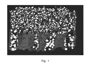
Fig. 1 shows an anode composed of tantalum metal powder that was produced by
the
method according to the invention. The differences in density within the anode
can be
clearly seen. There are three areas of very high porosity in the lower part of
the anode.
These are residues of non-irradiated powder from the powder bed. The remaining
area in
the lower part shows larger molten particles of differing density. The four
structures
pointing downwards serve as contact terminals for the capacitor. In the upper
part of the
anode, an extensive area (approx. 60% of the entire body) that has large
porous portions
can be seen.