Note: Descriptions are shown in the official language in which they were submitted.
84985677
METHODS AND APPARATI FOR MAKING THIN SEMICONDUCTOR BODIES FROM
MOLTEN MATERIAL
[0001] This application is a divisional of Canadian Patent
Application No. 2962682 filed on March 29, 2017, which is a
divisional of Canadian Patent Application No. 2754880 filed on
March 9, 2010.
INTRODUCTION
[0002] Inventions disclosed herein are methods of making a sheet
of silicon, which may later be used as a preform that is
recrystallized to produce a high quality substrate for the
manufacture of silicon solar cells. Other inventions disclosed
herein are methods for making a thin sheet of silicon that can be
used for manufacture of solar cells without recrystallization.
Methods disclosed herein may also be used to make thin sheets from
molten semiconductor materials other than silicon.
[0003] Processes are disclosed in Patent Cooperation Treaty
Application No. PCT/U52008/008030, entitled, RECRYSTALLIZATION OF
SEMICONDUCTOR WAFERS IN A THIN FILM CAPSULE AND RELATED PROCESSES,
filed June 26, 2008, in the names of Emanuel. M. Sachs, James G.
Serdy, and Eerik T. Hantsoo and the Massachusetts Institute of
Technology, designating the United States of America, and also
claiming priority to a provisional United States application,
No. US 60/937,129, filed June 26, 2007. The technology disclosed in
these applications can be used to recrystallize a semiconductor to a
different crystal form and is referred to herein as Recrystallization
In a Capsule (RIC) technology. Methods disclosed herein can be used to
make the starting material semiconductor sheet preform, which is
later recrystallized using RIC technology.
- 1 -
CA 3031880 2019-01-30
84985677
[0004] Certain processing schemes and architecture are
disclosed in Patent Cooperation Treaty Application
No. PCT/US2008/002058, entitled, SOLAR CELL WITH TEXTURED SURFACES
Filed: February 15, 2008, in the names of Emanuel M. Sachs and
James F. Bredt and the Massachusetts Institute of Technology,
designating the United States of America, and also claiming
priority to two provisional United States applications,
No. US 60/901,511, filed Feb. 15, 2007, and No. US 61/011,933,
filed Jan. 23, 2008. The technology disclosed in these applications
is referred to herein collectively as Self Aligned Cell (SAC)
technology. Methods disclosed herein can be used to make textured
semiconductor wafers for use as a starting workpiece for self-
aligned cells disclosed in the SAC patent applications.
SUMMARY
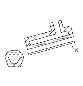
[0005] In one embodiment of a method disclosed herein, a
melt of silicon 13 is maintained and a cool sheet 15 of porous
refractory material, such as graphite, is passed over the melt
so that the refractory material contacts the top 15 of the
melt. A vacuum 17 is applied to the top of the porous
refractory sheet so as to pull the ambient atmosphere through
the sheet. Upon contact with the melt, two events take place
essentially simultaneously: 1) the silicon freezes to the
cooled surface of the porous refractory sheet; and 2) the
vacuum holds the silicon to the refractory sheet. The result is
a thin sheet 19 of silicon on a cool refractory substrate. The
silicon may be released from the refractory sheet after
releasing the vacuum 17. There is little or no adhesion to the
refractory sheet 5, as the refractory sheet was cool upon
contact to the silicon melt 13. The method may be used to form
thin sheets of other semiconductors in
- 2 -
Date Recue/Date Received 2021-07-16
84985677
addition to silicon. The following discussion uses silicon as an
initial example and generalizes this later.
[0005a] According to one aspect of the present invention, there
is provided an apparatus for fabricating a semiconductor body, the
apparatus comprising: a mold sheet, comprising a back surface and a
forming surface, wherein the forming surface is: i. porous such that
a plurality of open cell portions extend from the forming surface to
the back surface; ii. refractory; iii. planar; and iv. resistant to
degradation by molten semiconductor; and wherein the back surface is
spaced from the forming surface and defines a region in which a
first pressure can be established which is lower than a second
pressure at the forming surface such that a pressure differential
can extend through the open cell portions from the forming surface
to the back surface.
[0005b] According to another aspect of the present invention,
there is provided a semiconductor wafer comprising crystal grains
having nucleation sites that are spaced at regular intervals across
the lateral extent of the wafer surface.
BRIEF DESCRIPTION OF THE DRAWINGS
[0006] Fig. 1 is a schematic representation of a plenum and
refractory mold sheet for use with inventions hereof;
[0007] Fig. 2 is a schematic representation of such a plenum
with a refractory mold sheet having a textured surface;
[0008] Figs. 3A, 3B, 3C and 3D are a schematic representation of
method steps of an invention hereof using a plenum such as shown in
Fig. 1, with Fig. 3A showing a refractory sheet contacting a melt
surface; Fig. 3B showing a sheet of semiconductor formed on the mold
sheet; Fig. 3C showing the plenum and mold sheet assembly removed
from the melt and Fig. 3D showing the formed semiconductor sheet
- 3 ¨
Date recue/Date Received 2020-08-28
=
released from the mold sheet upon release of the vacuum in the
plenum;
[0009] Figs. 4A, 4B, 4C and 4D are a schematic
representation of method steps of a semi-continuous embodiment"
of an invention hereof using a plenum such as shown in Fig. 1,
with Fig. 4A showing a refractory sheet approaching a melt
surface that extends above beyond the edges of a crucible; Fig
4B showing a sheet of semiconductor forming on the mold sheet
as the mold sheet moves across the surface of the melt; Fig. 4C
showing the plenum and mold sheet assembly removed from the
melt after having passed beyond it; and Fig. 4D showing the
formed semiconductor sheet released from the mold sheet upon
release of the vacuum in the plenum;
[0010] Figs. 5A, 5B, 5C and 5D are a schematic
representation of method steps of another semi-continuous
embodiment of an invention hereof using a plenum such as shown
in Fig. 1, similar to that shown in Figs. 4A-4D, but with the
plenum passing past the melt surface such that the mold sheet
surface is inclined with respect to the melt surface, with Fig.
5A showing a refractory sheet approaching a melt surface; Fig
5B showing a sheet of semiconductor forming on the mold sheet;
Fig. 5C showing the plenum and mold sheet assembly removed from
the melt; and Fig. 5D showing the formed semiconductor sheet
released from the mold sheet;
10011] Fig. 6 is a schematic representation of a plenum and
refractory mold sheet such as shown in Fig. 1, with a backing
reinforcing the refractory sheet;
[0012] Figs. 7A, 7B, and 7C are a schematic representation
of method steps of an invention hereof using a plenum such as
shown in Fig. 1 with a mold sheet that has a very large scale
texture so as to provide a semiconductor sheet with such a
large scale texture, with Fig. 7A showing a textured refractory
sheet; Fig. 7B showing the textured refractory sheet with a
conforming shell of semiconductor adhered thereto; and Fig. 7C
-4--
CA 3031880 2019-01-30
showing the formed, textured semiconductor sheet released from
the mold sheet.
[0013] Figs. B A-E show schematically, in cross-sectional
view five stages of a method and apparatus that withdraws a
mold forming surface from nearly face-to-face contact with a
=
surface of a melt of molten material, and spins the mold
surface causing molten material to accumulate at edges of the
forming surface;
[0014] Figs. 9 A-C, show, schematically in cross-sectional
view, three stages of a method and apparatus that introduces a
mold forming surface to a surface of a melt of molten material,
by tilting the forming surface down toward the melt surface, to
establish, progressively, nearly face-to-face contact;
[0015] Figs. 10,A-E, schematically in cross-sectional view,
five stages of a method and apparatus that withdraws a mold
forming surface from nearly face-to-face contact with a surface
of a melt of molten material, by tilting the forming surface
away from the melt surface while molten material accumulates at
an edge of the forming surface;
[0016] Fig. 11 shows, schematically, a crucible with a rim
of partially submerged graphite;
[0017] Fig. 12 shows, schematically, a crucible with
submerged baffles for suppression of wave motion;
[0018] Figs. 13A and 13B show, schematically in cross-
sectional view, two stages of a method and apparatus, showing
detaching a meniscus of molten material from a formed
semiconductor body with a meniscus control element that is
above the free surface of the melt and that is not wetted by
the molten material;
[0019] Figs. 14A and 14B show, schematically in cross-
sectional view, two stages of a method and apparatus, showing
detaching a meniscus of molten material from a formed
-5-
CA 3031880 2019-01-30
=
semiconductor body with a partially submerged meniscus control
element that is not wetted by the molten material;
[0020] Fig. 15 shows, schematically, a cross-sectional view
of a crucible with a raised slot through which molten material
can be pumped, located within a crucible, for presenting to a
mold forming surface a locally protruding liquid surface;
[0021] Fig. 16 shows, schematically, a cross-sectional view
of a crucible with a raised, moving weir over which molten
material can flow, for presenting to a moving mold surface a
locally protruding liquid surface;
[0022] Figs. 17A and 17B show, schematically, two stages of
a method and an apparatus for providing a raised bump in a
melt, using magnetohydrodynamic principles.
[0023] Fig. 18 shows, schematically, a seed crystal for
growing crystals with relatively large grain size;
[0024] Fig. 19 shows, schematically, a relatively larger,
relatively weaker vacuum plenum with a moving, relatively
smaller, relatively stronger vacuum plenum located therein;
[0025] Fig. 20 shows, schematically, a cross-sectional view
of a mold sheet having a mold surface, with blind holes facing
toward the plenum, for localized vacuum profile control;
[0026] Fig. 21 shows, schematically, a cross-sectional view
of a mold sheet having a forming surface, with regions of
different thermal conductivity, for localized vacuum profile
control;
[0027] Figs. 22A and 223 show, schematically, in cross-
sectional view, two stages of a method and apparatus that
provides a mold adjacent a melt of molten material, which mold
is then moved, vertically past a melt surface such that a body
solidifies against the mold;
-6-
CA 3031880 2019-01-30
*
[0028] . Figs. 23A and 233 show, schematically in cross-
sectional view, two stages of a method and apparatus that
' introduces a mold vertically into a melt of molten material;
[0029] Fig- 24 shows, schematically, in cross-sectional
view, a method and apparatus that provides a mold with a
quantity of molten, material above it, and a vacuum pulling from
the opposite side of the mold sheet, generally below it;
[0030] Fig. 25 shows, schematically, in cross-sectional view
a mechanism of ejector pins for detaching a formed solidified
body from a mold surface;
[0031] Fig. 26 shows, schematically, in cross-sectional view
a mechanism of a stripper plate for detaching a formed
solidified body from a mold surface;
[0032] Fig- 27 shows, schematically, in cross-sectional
view, a dual plenum assembly, for use aiding securing a mold
sheet to a mold assembly, and also releasing a formed wafer
from a mold sheet;
[0033] Fig. 28 shows, schematically, in cross-sectional view
a mold surface that extends beyond a region of relative vacuum
application, to result in a solidified body that is smaller in
areal extent than a mold surface;
[0034] Fig. 29 shows, schematically, in cross-sectional view
a mold surface that has curved edges, to result in a solidified
body that is more easily detached from a mold surface;
[0035] Fig. 30 shows, schematically, a porous mold composed
of several layers of different materials and different
thickness;
[0036] Fig. 31A shows, schematically, a cross-sectional view
of a porous mold sheet with surface texture;
[0037] Fig. 313 shows the porous mold sheet of Fig. 31A,
with a relatively light vacuum having been applied, generating
-7-
CA 3031880 2019-01-30
relatively small amount of contact area between the mold
surface and the molten molding material;
[0038]. Fig. 31c shows the porous mold sheet of Fig. 31A,
with a relativelY strong vacuum having been applied, generating
relatively larger amount of contact area between the mold
surface and the molten molding material;
[0039] Figs_ 32A, 32B, 32C, 32D and 32E show, schematically,
steps of a method for providing and using a functional material
on the surface of the molten material;
[0040] Figs. 33A, 33B, 33C, 33D, 33E, 33F, 33G and 331! show,
schematically, steps of a method for growing a sacrificial
wafer, growing a functional material upon the sacrificial
wafer, melting away the sacrificial wafer, leaving the
functional material from the wafer on the melt surface,
contacting a mold forming surface to the melt at the functional
material and solidifying a formed wafer at the forming surface
and removing the formed wafer from the mold surface;
[0041] Fig. 34 shows, schematically, a cross-sectional view
of a substrate, typically silicon, with conical through holes;
[0042] Fig. 35 shows, schematically, a cross-sectional view
of a substrate, typically silicon, for use as a mold sheet
having a mold surface, with laser cut, powder filled holes;
[0043] Fig. 36 shows, schematically, a cross-sectional view
of a substrate, typically silicon, for use as a mold sheet'
having a mold surface, with a porous silicon internal portion,
partially oxidized, and a porous SiO, outer layer(s);
[0044] Fig. 37 shows, schematically in flow chart form steps
of a method of an invention hereof for making a microporous
silicon substrate using an electroless application of a metal
seed layer and laser augmentation; and
[0045] Fig. 38 shows, schematically, a cross-sectional view
of a substrate, typically silicon, for use as a mold sheet
-8-
CA 3031880 2019-01-30
having a mold surface, with a bulk silicon internal portion,
pierced by oxidized porous silicon plugs and a bulk SiO2 outer
layer(s).
DETAILED DESCRIPTION
[0046] General aspects of inventions disclosed herein are
discussed first. Following the general aspects, detailed
variations are discussed.
[0047] An aspect of an invention hereof will first be
discussed in a batch implementation, where a single
semiconductor sheet is made at a time, as shown schematically
with reference to Figs. 3A-3B. In this case, the semiconductor
melt 13 may be contained in a fairly conventional crucible 11
made of graphite, silica, silicon carbide, silicon nitride and
= other materials known to 'contain molten silicon. As shown in
Fig. 1 in detail a vacuum plenum 1 is created, for example, by
machining a cavity 3 into a block of graphite. A thin sheet 5
of graphite is affixed to the bottom bf the plenum 1. This
sheet preferably has a fair degree of gas permeability (having
a high porosity and/or being relatively thin). The plenum is
preferably the least porous graphite available. The plenum
could also be made of non-porous ceramic. The thin sheet will
be referred to herein as the mold sheet. Vacuum suction is
applied at port 7. The assembly 8 of plenum 1 and mold sheet 5
is supported from above by a structural member (not shown). An
extension of vacuum port 7 may act as this structural member,
or a separate structural member may be provided. Referring now
to Fig. 3A, the assembly 8 is brought into contact with the
surface 15 of melt 13 as in Fig. 3A. The assembly is allowed
to remain in contact with the melt for a designated period of
time, perhaps on the order of 1 second. The amount of contact
time between the assembly and the melt will vary depending on
factors that include, but are =not limited to: the temperature
of the melt, the temperature of the mold sheet, the thickness
of the mold sheet and the intended thickness of the silicon
sheet to be fabricated. A silicon sheet freezes onto the mold
-9-
CA 3031880 2019-01-30
sheet, as shown in Fig. 3B because the mold sheet 5 is colder
than the freezing point of the silicon. The process is thus a
transient heat transfer resulting in the silicon melt 13 being
cooled to the melting point and then heat of fusion being
extracted, resulting in the buildup 19 of solid silicon on the
mold sheet. In general, the mold sheet should be kept colder
than the freezing point of the molten material. Even more
generally, at least a portion of the mold sheet should be at a
temperature below the freezing point, for at least a portion of
=
the time that the mold sheet contacts the molten material.
Taking silicon as an example, the freezing/melting point is
1412 C). useful ranges for maintaining the mold sheet might go
from room temperature to 1300 C, with likely range from 900 C-
1200 C, but any temperature below the freezing/melting point
may be suitable, depending on the totality of the
circumstances.
[0048] A principal purpose of the vacuum is to cause the
silicon sheet 19 to be temporarily held against the mold sheet
5. It is helpful that the silicon sheet 19 be easily removed
from the mold sheet 5 after the silicon sheet is formed. It is
very helpful if the silicon sheet would simply fall off.
However, it is very important that as the silicon sheet is
being formed, it adhere to the mold sheet 5. The vacuum 17
accomplishes this goal. without the vacuum, when the mold
sheet is removed after being in contact with the molten silicon
13 for the appropriate length of time, the solidified silicon
19 would likely remain behind on the top 15 of the melt and
then it would remelt. Indeed, significant adhesion is needed
to remove the solidified silicon sheet 19 from the melt 13, 15
because the surface tension of the molten silicon is holding
the silicon sheet 19 down.
[0049] After the designated period of time, the assembly 8
is lifted out of the melt 13, now carrying silicon sheet 19
attached to it, as shown in Fig. 3C. Finally, in Fig. 3D, the
vacuum 17 is released and the formed silicon sheet 19 can be
separated from the mold sheet 5. Upon release of the vacuum 17
-10--
CA 3031880 2019-01-30
the silicon sheet 19 may simply fall off. However, some small
amount of residual adhesion may keep the sheet from falling
off. One approach is to apply positive gas pressure to the
plenum of assembly 8, so as to blow sheet 19 off. Another is
to provide some gentle mechanical removal. Techniques for this
are discussed in detail below.
[0050] The graphite mold sheet 5 must have sufficient
porosity to allow for suction sufficient to accomplish the goal
of adhering to the silicon sheet 19. There are a very large
variety of grades of graphite, ranging over a very large range
of porosity. Thus there are many suitable choices. Two such
suitable choices are Grade pm6 and Grade 2191, both from Ultra
Carbon Corporation of Bay City Michigan, a division of Carbone
of America. Lower porosity graphites can also be used by
making a mold sheet 26 thin so as to allow sufficient flow of
gas through it. As shown schematically with reference to Fig.
6, if the mold sheet 26 is too thin to support itself over its
full width while under vacuum, backup structure 29 may be
provided within the plenum. This structure may be machined
into the plenum in the form of ribs and posts. Alternatively, a
piece of very porous graphite or other porous material may be
placed in the plenum to provide backup support. For example,
extremely high porosity can be attained using ceramic filter
bodies, which are known in the art.
=
[0051] The porosity of the mold sheet 5 must not be so great
as to allow the molten silicon 13 to enter the pores, thereby
making release of the silicon sheet 19 difficult or impossible.
Two independent factors combine to prevent silicon from
entering into fine pores. First, the surface tension of the
molten silicon is too high to permit it to infiltrate fine
pores (of a non-wetting material). Second, the silicon is
beginning to freeze rapidly on contact to the mold sheet and
this freezing would be especially fast in the high surface area
to volume ratio situation presented by a fine pore. The second
factor is present even for a wetted material.
-11-
CA 3031880 2019-01-30
[0052] An advantage of lower porosity graphite for the mold
sheet is that the grain size of this material is smaller and
the material can therefore allow for fine finishes on the
formed silicon sheet. These finishes can be nearly mirror-like
and provide for a very smooth silicon sheet. Alternatively, as
shown in Fig. 2, a graphite sheet 35 may have texture 9
deliberately machined into mold sheet 5, with the intent of
transferring the texture to the formed silicon sheet. This
texture can then act to trap light and also to provide the
grooves needed to accomplish manufacturing operations of the
cell, such as are described in the SAC patent applications
mentioned above, such as channels for metallization, such as
conductive fingers, and bus-bars. The application of vacuum
draws the silicon melt to fill relevant texture elements, such
as grooves, channels, etc. The vacuum suction needs to
overcome the surface tension of the molten silicon to fill a
texture element. The texture element can be modeled as a
hemisphere. It follows that the smallest hemispherical texture
element that can be filled can be estimated by applying
Laplace's equation, as follows:
Pressure = 1 atm = 2 y/r
Where y is the surface tension of the molten silicon and r is
the radius of the hemispherical texture. For silicon with
y=.72 N/m, r = 7 microns. This is sufficiently small to allow
for good light trapping, especially since the texture can be
larger than with an etched texture (since no silicon needs to
be etched/wasted). The feature sizes of the metallization
grooves are larger than those of the light trapping features,
and thus, the metallization grooves are easier to fill with
molten material. In fact, the light trapping texture can be
done at a very large scale. The topography of the top surface
can have a characteristic feature scale that can be deeper than
the thickness of the wafer itself. The foregoing discussion
relates to using a melt surface at approximately atmospheric
pressure. Below, variations are discussed using a melt surface
at higher than atmospheric pressure, which would permit
-12-
CA 3031880 2019-01-30
achieving smaller hemispheric texture elements than is
discussed above.
[0053] Figs. 7A, 713 and 7C show a mold sheet 31 with large
scale texture- The scale of this texture is larger than the
intended thickness of the silicon sheet to be formed. Fig. 7B
shows the mold sheet and plenum assembly with the frozen
semiconductor sheet 32 in place. Pig. 7C shows the silicon
semiconductor sheet 32 after release from the mold sheet. As
shown, the amplitude of the corrugations .of the formed sheet 32
is at least three times the thickness of the sheet 32 itself.
[00541 One important issue is that when the frozen layer is
lifted out of the melt, some liquid may stick to the bottom and
then freeze in a way so as to make the bottom lumpy. One
method to minimize this is to lift the mold sheet up one edge,
or corner first, thereby allowing molten material to run off
the bottom of the wafer and back into the bulk of the melt.
=
[0055] The rapid disengagement of the freezing semiconductor
sheet from the bulk of the liquid can be aided by lifting the
mold sheet up a few millimeters (up to approximately 10 mm is
possible without meniscus detachment) iMmediately after contact
with the melt. This will establish a meniscus of liquid, which
will more readily drop off when the mold sheet is raised at the
end of solidification. The steps of tilting the formed semi-
conductor sheet to minimize excess liquid attachment are
discussed in more detail below.
[0056] Another approach to removing any residual liquid from
the underside of the formed semiconductor sheet upon withdrawal
is to rapidly spin the mold sheet and attached semiconductor
sheet thereby throwing the residual molten material off to the
side. This can be practiced with a square shaped mold sheet.
However, for symmetry, a round mold sheet may be used,
resulting in the casting of a disk shaped semiconductor sheet
wafer. This wafer could then be laser trimmed to desired shape
and size and the cut off pieces re-melted. The spinning of
the mold sheet and wafer could commence immediately upon
-13-
CA 3031880 2019-01-30
detachment of the meniscus, which is effected by raising the
mold sheet. Alternatively, commencement of rotation could be
the means by which meniscus detachment is effected. The liquid
laterally ejected by spinning could be allowed to impact into
' the side-walls of the containing crucible and drip back in to
the melt. Alternatively, if only a small amount of liquid is
ejected it may be desirable to allow this liquid to be flung
over the edges of the crucible to remove them from the melt.
These droplets of liquid would impact a cold surface and freeze
to it for later removal during planned maintenance. This bit
of liquid will have concentrated impurities in it due to the
segregation of impurities during the solidification. Thus
removing this liquid will remove impurities from the system.
The steps of spinning the formed semiconductor sheet are
discussed in more detail, and illustrated below.
[0057] It may be desirable to raise the temperature of the
mold sheet up to as high as, for instance, 1200 C, or as high
as it can be, while still avoiding any adhesion between silicon
and mold sheet. A higher temperature mold sheet will result in
slower heat transfer and larger grain size in the solidified
semiconductor sheet. Further, in the single wafer batch mode
now under discussion, it may be desirable for the
solidification to take as long as 5 seconds to provide for
easier control over the process. Further, it may be desirable
to control a temperature profile across the mold sheet so as to
cause the solidification to proceed from one point or side on
the mold sheet to another, resulting in larger grains. For
example, with a circular mold sheet it may be desired either to
have the center hotter than the perimeter or the perimeter
hotter than the center, depending on the desired direction of
grain growth. Having the initial nucleation at the perimeter
may be advantageous because these small grains would then be
cut off during the trimming operation.
[0058] One means of effecting temperature control over the
mold sheet is to hold it in position 1-2 cm above the melt so
that it can gain heat and then blow argon out through the mold
-14-
CA 3031880 2019-01-30
sheet (via the port that will later be used to apply vacuum) so
as to provide cooling and control the temperature of the sheet.
If the thickness of the mold sheet is varied over its extent,
the flow through it will vary. where the mold sheet is
thicker, there will be less flow of cooling gas and the mold
sheet will run hotter. Another advantage of blowing argon out
the mold sheet while it is in position above the surface of the
melt is that it will keep vapor such as silicon oxides, from
depositing on the mold sheet.
[0059] The frozen formed semiconductor sheet may be released
from the mold sheet simply by removal of vacuum. In addition,
some outward flow of gas can be imposed to help separate the
formed semiconductor sheet. Further, the application of
pressure within the plenum so as to cause outward flow of gas
can also be used to cause the mold sheet to bow out slightly
and controllably, thereby helping to separate the formed
silicon semiconductor sheet. These and additional methods to
encourage detachment are discussed in more detail below.
[0060] In another preferred embodiment, the mold sheet is
continually moved laterally over the surface of a pool of melt.
While it is possible that the mold sheet be a belt and that the
process be continuous, it is also possible to be practiced with
mold sheets of discrete length, for instance on the order of .5
¨ 2 meters long. This mode will be referred to herein as a
semi-continuous mode.
[0061] A differentiating requirement of a continuous and a
semi-continuous modes of operation is that a melt contained
within and below the walls of a crucible will not, without
something else, suffice for a continuous or semi-continuous
mode, because the mold sheet larger than the crucible cannot
contact the melt without interfering with the crucible walls.
One solution is to create a bump in the melt, much as in wave
soldering. This can be done by pumping the melt up through a
slot and letting the melt overflow the slot and fall back down
into the main pool of melt. Molten silicon can be pumped with a
-15-
CA 3031880 2019-01-30
centrifugal pump, immersed in the melt. Alternatively, an
oscillating magnetic field, such as created from a coil placed
below the melt, can cause the melt to mound up due to
electromagnetic repulsion. Magneto-hydrodynamics can be used
to create a bump in the melt surface, by passing a current
laterally in the melt and imposing a perpendicular magnetic
field, to cause an upward body force on the melt. Each of these
methods is discussed in more detail below, and is illustrated '
with reference to figures of the drawing.
[0062] Another method for allowing the mold sheet to contact
the surface of the melt in either a continuous or semi-
continuous mode is shown in Figs. 4A, 4B, 4C and 4D. The melt
23 is provided in a narrow trough 21 and the top of the melt
extends over the top of the trough. The degree of extension
can be small, about, 1 to about 4 mm. The melt will remain in
place due to capillary action and will not overflow the trough.
Fig. 4A shows the mold sheet in assembly 8 prior to arrival at
the melt 23. Fig. 4B shows the mold sheet 5 approximately
midway through its traverse over the melt with a thickness of
silicon 19 frozen to the portion of the mold sheet 5, which has
emerged from contact with the melt. The center portion of the
mold sheet is still in contact with the melt and here silicon
is in the process of freezing to the mold sheet. The
consequence is that the interface 21, which demarks the
boundary between liquid and solid, is inclined at an angle a
relative to the bottom surface of the mold sheet 5 (indicated
by the extension of the upper line bounding the angle x). Fig.
4C shows the mold sheet 5 and vacuum assembly 8 after it has
completed its traverse, with the silicon sheet 19 still
attached by vacuum 17. In Fig. 4D the vacuum 17 has been
released and the silicon sheet 19 removed.
[0063] The speed of traverse of the mold sheet over the melt
can be quite rapid. The contact time with the melt can vary
between .001 and 1 second or more, for instance two seconds.
If the contact width is 2 cm, the corresponding traverse speeds
-16-
CA 3031880 2019-01-30
will be 20 m/s and 2 cm/s, with speeds in the range of between
about 5 ¨ 20 cm/s most likely.
(0064) The heat of fusion for silicon is 1787 Jig, compared
to a specific heat of 0.7 J/gK. The energy required to
solidify a superheated melt is overwhelmingly dominated by the
heat of fusion, since even with 100 K superheat, the sensible
heat accounts for only 4% of the energy required to freeze.
Since the process and resulting film thickness are controlled
by heat transfer, the process is very tolerant to variations in -
melt temperature. To solidify a 200 micron thick film, the
energy required per unit area (based on heat of fusion only) is
90 J/cre. For a high thermal conductivity substrate, the heat
extraction is dominated by the heat transfer coefficient
between the mold sheet and the semiconductor (e.g. silicon).
As an example, typical heat transfer coefficients for rapid
solidification processes are 1 x 10³ to 1 x 10⁶ W/m2K, with an
experimental value for silicon on a water cooled copper and
stainless steel wheel determining by uno as 4.7 x 10² W/m3K.
Heat flux per unit area is defined as: Q/A = h (Tmeit Tsubstrate)'
[0065] For a 1000K temperature gradient, heat flux of 470
Wien2 would result in a solidification time of -200 ms for a
thickness of 200p.m. As a check to confirm the substrate
:thermal conductivity will not limit heat flow, the thermal
diffusivity of graphite is approximately 0.1 cre/s, resulting in
thermal diffusion length of 1.4 mm in 0.2 sec. Assuming the
energy of solidification is taken up by a 1 mm thick surface
layer of graphite with a specific heat of 2 J/gK, would result
in a temp rise of 200K in the graphite during Lhe molding
event.
[0066] In many embodiments, it will be important to keep the
amount of melt available in the trough approximately constant
during the traverse of the mold sheet, thus requiring that melt
be admitted to the trough-. This melt can come from a large
reservoir of molten silicon that is contained in a crucible
connected to the trough. The larger the reservoir, the smaller
-17-
CA 3031880 2019-01-30
=
the change in melt height in the trough during a traverse.
Further control of melt height can be achieved by using a
displacer piston, for example of graphite, to compensate for
the silicon withdrawn during a traverse, the piston being moved
downward.
[0067] While transient heat transfer will determine a
thickness of silicon sheet that will freeze to the mold sheet
during the period of contact with the melt pool, some amount of
liquid silicon may also be drawn off on the underside of the
solidified silicon. To prevent this, the mold sheet may be
traversed over the melt pool at an angle with respect to the
horizontal as shown schematically in Figs. 5A, 5B, 5C and 5D.
This will provide a small hydrostatic head, which will drain
any liquid silicon adhered to the bottom of the solidified
silicon 19, back into the melt pool. Figs. 5A, 5B, 5C and 5D
show the same moments in the process sequence as was described
with respect to Figs. 4A, 4B, 4C and 4D, respectively. Note
that the crucible 25 in Figs. 5A and 5B has inclined outer
walls. This inclination provides a margin of protection
against silicon wetting down the side wall of the crucible,
especially during the condition of Fig. 5B when the liquid is
being drawn off the edge of the crucible.
[0068] Another important benefit of these methods is the
ability to reject impurities into the melt and avoid having
them incorporated into the growing silicon sheet. Most
electrically harmful metallic impurities are much less soluble
in the solid than in the liquid and hence tend to be rejected
at the solidification interface. In crystal growth processes
where the liquid/solid interface moves in a controlled
direction ¨ such as is the case in these processes- this offers
the opportunity to purify the feedstock material. To be able to
segregate impurities back into the bulk of the melt, the rate
of advance of the liquid/solid interface must not be too high,
or impurities get frozen into the solidified material. While
the rate of formation of sheet is high in the inventions
disclosed herein, the rate of advance of the solidification
-18-
CA 3031880 2019-01-30
=
interface is significantly lower, owing to the angle a of
inclination of the liquid solid interface with respect to the
direction of pulling, indicated by the arrow P, which is also
parallel to the bottom surface of the mold sheet. For example,
consider where the width of the trough containing molten
silicon is 2 cm and where the length of time needed for contact
is .2 second. The pull speed is then 10 cm/sec. If the sheet
being fabricated is 200 microns thick (a typical thickness),
then the rate of advance of the solidification interface is 200
microns in 0.2 seconds, or 1 mm/sec. This rate of advance,
while high, will still allow for segregation and attendant
purification.
[0069] Segregation also impacts some intentional dopants and
in standard crystal growth methods, makes it difficult to use
such dopants. For example, gallium is a desirable p-type
dopant in silicon, but is ordinarily difficult to use because
segregation results in the resistivity of the grown crystal
decreasing as growth continues in an ingot growth or casting
process. The same is true for phosphorous, an n-type dopant.
However, with methods of the current inventions, dopant will
build up in the melt and reach a steady-state, which can be
maintained by proper replenishment of the melt. In this way,
each wafer is formed from a melt with the same level of doping
and thus will itself have the same level of doping. Also, the
formation of wafers directly from the melt enables close, rapid
process monitoring for bulk resistivity_ Any needed change in
melt dopant concentration can be effected rapidly, along with
each addition of Si feedstock.
[0070] The angle of inclination of the crystal growth
interface is due to the fact that most of the heat is removed
from the silicon across the thickness of the solidifying sheet
(perpendicular to the direction of traverse/pulling). As a
consequence, the temperature gradients in the solidifying sheet
can be very low. This will lead to low stresses within the
solidifying sheet and therefore low dislocation densities. As
dislocation density is a major factor degrading the electronic
-19-
CA 3031880 2019-01-30
performance of silicon sheet for photovoltaics, this is a major
advantage.
[0071] The mold
sheet 5 may be made of graphite, but also of
a range of other materials including, for example, silicon
carbide, silicon nitride, silica, boron carbide, pyrolitic
boron nitride and alloys of these including silicon oxynitride.
Because the mold sheet is kept cool it is also possible to
consider materials such as aluminum oxide (which would
otherwise lead to contamination of the melt by aluminum if
contacted to the melt while hot). Other materials, such as
silicon itself, are discussed below. In all cases, the porosity
required to allow for vacuum suction can be created by
fabricating the mold sheet from powder and either sintering or
otherwise bonding the powder together in a porous body. It is
also possible to make the mold sheet of a non-porous material
and provide a sufficient density and multiplicity of small
holes to admit the vacuum. In general, the mold sheet must
exhibit enough permeability to allow suction, but not enough to
admit silicon. It should not contain transition metals or
transition metallic impurities. It should be fabricated in a
thin sheet and either flat or with texture. It must tolerate
some degree of thermal stress/shock.
-20-
CA 3031880 2019-01-30
[0072] The foregoing has described, in general, that the
forming face of the mold sheet (also called a forming mold, in
some cases) be at a temperature that is below the melting point
of the semiconductor material. This must be so for a portion of
the area of the forming face, for a portion of the duration of
time that the forming face is in contact with the molten
material, but not necessarily for the entire time and over the
entire area of the forming face. Similarly, the foregoing has
described that a vacuum (or, as discussed elsewhere, a pressure
differential) be applied so that there is a pressure
differential between the back, non-forming face of the forming
mold, and the molten material, so that the molten material is
drawn or forced against the forming mold. However, this
pressure differential or vacuum need not be applied over the
entire surface area of the forming mold, or even the entire
portion that is in contact with molten material, or, for the
entire duration of time that the forming mold is in contact
with the molten material.
[0073] The processes described herein rely on differential
pressure applied between the face of the mold sheet 5 (Fig. 1)
exposed to the melt (the forming face, also called forming
surface 6) and the opposite face of the mold sheet (the back
face 4). A convenient means of applying this differential
pressure employs a vacuum pump to generate low pressure on the
back face 4 of the mold sheet, while using substantially
ambient-pressure gas at the melt surface 15 and thus the
forming face 6 of the mold sheet 5. An advantage of this
embodiment is that the furnace enclosure does not need to be
sealed gas-tight nor does it need to be capable of sustaining
positive pressures beyond what is required for purge gas
containment. However, in another embodiment differential
pressure between the faces of the mold sheet is generated by
venting the back face 4 of the mold sheet 5 directly to
atmosphere, while maintaining the atmosphere on the forming
face of the mold sheet at a pressure substantially higher than
local atmospheric pressure. An advantage of this embodiment is
-21-
CA 3031880 2019-01-30
that a vacuum pump is not required. A further advantage of
this embodiment is that trans-mold sheet differential pressures
greater than the local atmospheric pressure can be achieved,
which may confer process benefits, for example in the creation
of fine surface texture. The differential pressure may be
applied before the mold sheet contacts the surface of the
molten material, or after.
[0074] When the present specification and claims use the
term vacuum, it also corresponds to any means of developing a
pressure difference between the forming face 6 and back face 4
of the mold sheet 5, regardless of the absolute pressure at
either the forming surface. 6 or back 4 of the mold sheet 5.
Experimentally, differential pressures ranging from 1
kilopascal (kPa) to 100 kPa across the thickness of the mold
sheet 5 have demonstrated process viability. It should also be
noted that whenever the present specification and the claims
use the term vacuum, it is understood to mean a partial vacuum
of any degree, up to and including a complete vacuum.
POROSITY
[0075] The foregoing, and following, describe mold sheets
and forming mold bodies that are porous. By porous, it is meant
open-cell porosity, such that gas can flow through the porous
body from one surface to an opposite surface. Such porous
bodies may also include closed cell porous regions. It is
necessary that the overall body be porous in such a way as to
allow the transmission of gas therethrough. Thus, the term
porous is used herein to describe such porous bodies that allow
the transmission of gas therethrough, even though they may also
included closed cell portions.
[0076] The growth of the forming semiconductor wafer may
proceed in either a continuous, semi-continuous or discrete
mode, as discussed above. For continuous growth a mold sheet
must be fed over a rim or lip of a melt-containing crucible,
come into contact with the melt over a predetermined distance,
and then be fed out over a rim or lip of the crucible. A flat
-22-
CA 3031880 2019-01-30
mold sheet would require some portion of the melt to reside
above the lip of the crucible. This could be accomplished by
the formation of a mound or raised bump in the melt, by
mechanical pumping or magneto-hydrodynamic (MHD) forces, as
discussed above and also below. Or, molten material could
reside above the rim or lip of the crucible if the liquid
meniscus was pinned at the top edge of the crucible. This
crucible might be in the shape of a linear trough, such as
shown above with reference to Figs. 4A-4D and Figs. 5A-5D. Such
a trough could be free standing, or could reside in or above
another, larger crucible- This arrangement would have the
advantage of retaining any melt that was lost over the edge of
the trough crucible. A means of transferring melt from the
lower, larger crucible back into the trough may be useful to
minimize waste.
=
[0077] One
issue with discrete or semi-continuous growth, as
shown schematically with reference to Figs. 8A-8F is the
disposition of molten material remaining on the melt side
surface of the wafer after forming. A microporous mold sheet
805 suspended from a vacuum plenum assembly 808 that is dipped
into the melt 813 such that the forming face of the mold sheet
805 is substantially parallel to the free melt surface 815 and
then withdrawn in the direction of the arrow W, tends to form a
pendant drop 889 (Fig. 8D). This drop interferes with
subsequent wafer processing and is generally undesirable. One
method discussed above for removing this excess liquid, and now
= illustrated here is to spin the mold sheet 805 rapidly as
indicated by the arrow 5, upon withdrawal from the melt 813,
thereby throwing the excess liquid off the rim or segregating
it to the periphery 888 of the formed wafer 819 (Fig. 8E). This
method could be used with round or polygonal mold sheets 805.
Excess melt can be returned to the crucible or removed from the
system as a means of impurity rejection. Excess melt localized
to the rim or corners of a spinning planar substrate can be
trimmed off and returned to the crucible. AS with excess
liquid, some or all of this material may be sequestered as a
means of impurity removal. This excess'melt is likely to be
-23-
CA 3031880 2019-01-30
high in rejected impurities as it will be the last to freeze.
As shown in Fig. 8E, the axis of rotation of the mold sheet 805
is substantially normal to the plane of the formed wafer 819.
This need not be the case. Further, the axis of rotation is
shown to be vertical, relative to a gravitational field. This
also need not be the case.
[0078] Another method for dealing with a persistent drop of
molten material, illustrated schematically with reference to
Figs. 9A-9C and Figs. 10A-10E is to cause a drop 1088 to form
on one edge of the formed wafer 19, rather than in the center.
In this manner a sacrificial area of the wafer can be reserved
for the purpose of accommodating the drop, which can be cut off
of the formed wafer and fed back into the melt. One method for
achieving this is to tilt the entire vacuum plenum and attached
forming face at an angle to the melt surface. This approach
requires the use of a vacuum connection allowing the tilt
motion, and capable of operation at liquid silicon
temperatures, without release of contaminants that might
compromise final wafer quality.
[0079] One implementation of this method is in two stages.
The first stage is the lay-in (Fig. 9A-Fig. 9C), where the
forming face 6 is held at a tilt and translated down as
indicated by the arrow L, until contact with the melt surface
15 is made at the lower edge 985 of the forming face. The
entire vacuum plenum with attached forming face is rotated
about an axis parallel with the edge 985 of the forming face 6
in contact with the melt surface 15 in such a way as to sweep
the molten material across the forming face 6. The edge 985 of
the forming face that touched the melt surface may move
. vertically during this event. One consequence of this swept
introduction of the molten material to the forming face 6 is to
encourage lateral growth of the silicon wafer on the forming
face (parallel to the plane of the forming face) so as to form
an elongated grain structure with relatively large grains,
which is desirable. Subsequent freezing onto this large-grained
crystallographic template can occur normal to the surface of
-24-
CA 3031880 2019-01-30
the forming face 6. Associated with the swept introduction and
lateral growth is a liquid-solid silicon interface, which is at
an angle with respect to the plane of the wafer (much as shown
in Fig. 4B, but in that case in the context of a trough).
10080] It should be noted that the same apparatus can also
be used to introduce the forming face parallel to the surface
of the melt so that all portions of the forming face contact
the melt at the same time. In such a case, the interface
between solid and liquid silicon will be substantially parallel
to the plane of the forming sheet and of the wafer. Cases
where the forming sheet is brought down parallel to the melt
have the possibility of trapping small amounts of furnace
ambient gas between the forming sheet and the melt, however,
these small amounts of air will be removed by the vacuum which
is being drawn through the forming face.
[0081] If, as shown with reference to Figs. 10A-10E, the
forming surface 6 is tilted as the mold sheet 5 is removed from
the melt surface 15 the liquid meniscus 1087 can be shed in a
controlled manner, and any residual melt 1088 left at the edge
1089 of the formed wafer 19 (Fig. 10E). This has the advantage
of sweeping the meniscus in a linear manner across the wafer
surface, leaving behind only a very thin film of molten
material. As with the spinning arrangement, the excess or
segregated material may be trimmed off and returned to the
melt; with some of the trimmed material sequestered for removal
of impurities from the melt and crucible.
[00821 The surface finish, including flatness and
smoothness, of the silicon wafer is determined in large part by
the shedding of the liquid meniscus after growth of the wafer.
Good surface finish may be attained by the tilting motion
described above but other processes may also further improve
surface finish. One important factor in the detachment of the
liquid meniscus is the motion of the melt during .the shedding
of the liquid from the wafer surface, for instance by tilting,
or spinning the formed wafer, as described below. A controlled,
-25-
CA 3031880 2019-01-30
slow, smooth retraction of the wafer from the liquid leads to a
smooth wafer surface. Instability of the liquid meniscus during
shedding, as for example caused by waves in the melt, can lead
to adverse surface artifacts, such as ripples and bumps, on the
surface of the wafer.
(0083] One method to improve the surface finish of the wafer
is to reduce the amplitude of any wave motion of the melt, and
rapidly damp any waves that do occur. One method for reducing
wave amplitude is to use a shallow melt 13 (Fig. 3A), for
example a melt depth of 5 mm or less is useful, and even as
shallow as 3 mm or 1 mm, if local particulate impurities on the
crucible bottom are not larger than about .5 mm. The minimum
melt depth achievable for certain non-wetting crucible 11
materials, such as quartz, is dictated by the surface tension
of liquid silicon and the contact angle between liquid silicon
and the crucible material. As a result, to obtain very shallow
melt depths in such materials, a rim of wetting material may
also be included to ensure full areal coverage of the crucible.
For example, as shown schematically with reference to Fig. 11 a
thin (e.g. 5 mm thick) ring 1112 of graphite (which is wetting
for silicon) can be used, with an outer diameter that matches
the inner diameter of the crucible 11, and a height equal to
the desired depth of the melt 13.
[0084] Another method for reducing waves in the melt, shown
schematically with reference to Fig. 12 is to use physical
baffles 1214 submerged below the surface 15 of the melt 13.
These baffles impede lateral flow of liquid and quickly damps
out any wave motion present in the melt.
[0085] Another means of controlling the rate of removal of
melt from the formed wafer surface may be a meniscus control
element_ This consists of a separate body that is moved
relative to the forming face and the position of which controls
the position of detachment of the meniscus from the freshly
formed wafer surface.
-26-
CA 3031880 2019-01-30
[0086] This topic discusses the stability of a meniscus
attached to a forming face that is parallel to but raised from
the nominal free melt surface. The equilibrium wetting angle of
a liquid on a solid surface is determined by the surface
energies of the melt and the Surface. This angle is repeatable
and is considered to be a constant for a given system of
liquid, solid, and ambient gas. The equilibrium angle of
attachment of liquid silicon on solid silicon in an inert gas
is 11 degrees. Should a physical situation exist where the
wetting angle is perturbed to less than 11 degrees then the
meniscus attachment point will tend to move until equilibrium
is re-established and the angle of attachment is 11 degrees.
The case of attachment of the liquid meniscus to the horizontal
forming face (held parallel to the free melt surface) may be
examined by using Laplace's equation, which relates the
pressure difference across a liquid-gas or liquid-liquid
interface, the radii of curvature of that surface, and the
surface energy of that interface. The pressure across the
interface can be taken as the hydrostatic pressure:
P = pgH
(liquid density*gravity*height from free surface). The ambient
gas pressure is taken as a constant in this calculation, and is
considered to be equal to the pressure in the liquid at the
free melt surface.
[0087] If a linear edge of attachment is considered then
there is only one radius of curvature, and Laplace's Equation
becomes
P = 2y/r.
By assuming an angle of attachment and incrementing along the
surface in Very small steps of swept angle the associated
pressure drop and change in curvature can be solved for
numerically. It was found through iteration that the maximum
stable height of the forming face above the free melt surface
-27-
CA 3031880 2019-01-30
was about .01077 m. A density value of 2530 kg/m3 and a surface
tension of 0.72 N/m was assumed.
[0088] In the case of a forming face being slowly raised
from the free melt surface the following can .be predicted. As
long as the attachment angle of meniscus to forming face is
greater than 11 degrees the system is stable and the liquid 813
remains attached to the edge of the forming face. Once the
forming face is raised to the height where a further increase
in height would demand an angle of attachment of less than 11
degrees to the flat surface of the forming face, the meniscus
887 moves laterally until equilibrium is re-established or
until the traveling meniscus from the other edge of the forming
face is met. In this case the contact between the melt and the
forming face is lost, and a large remaining droplet 889 is left
on the forming face (Fig. 8D). Very small perturbations in the
height of the melt can vary the velocity of detachment of the
meniscus, or even reverse it temporarily. These perturbations
can be caused by waves in the melt; which are difficult to
avoid in a container of liquid (crucible) subject to agitation
by the action of the vacuum plenum and forming face.
[0089] Control of the velocity of meniscus detachment is
desirable, as it has been observed that the surface finish of
Si sheet formed by this technique is highly dependent on the
relative speed of withdrawal of the meniscus from the sheet
surface- Techniques that better control the speed of withdrawal
of the meniscus from the surface of the freshly formed Si sheet
are well suited to control the surface finish of the Si sheet.
[0090] The above discussion of stability of meniscus
attachment pertains to the control of detachment velocity of
the meniscus from the Si sheet. One means of controlling the
rate of removal of melt from the formed wafer surface may be a
meniscus control element. This consists of a separate body that
is moved relative to the forming face and the position of which
controls the position of detachment of the meniscus from the
freshly formed wafer surface.
, -28-
CA 3031880 2019-01-30
[0091] One configuration of meniscus detachment mechanism
uses a material that is not wetted by the melt. The material
should have a wetting angle of greater than approximately 60
degrees with respect to the molten material in the ambient
atmosphere present. Figs. 13A and 13B show one possible
implementation of such a mechanism. In this example, a wafer 19
is formed by dipping the mold sheet 5 into the melt 1313. After
growth of the wafer, the mold sheet 5 is retracted above the
free surface 1315 of the melt 1313, to such a height that the
liquid meniscus 1387 is still attached to the melt side of the
formed wafer 19 (less than .01077 m per the above example).
The meniscus control element, for instance, consisting of a
horizontal cylinder 1391 of small diameter (for example 5 mm),
is translated between the formed wafer 19 and the melt 1313, in
the direction indicated by the arrow M, forcing the detachment
of the liquid meniscus 1387 from the solid silicon wafer 19.
This occurs due to deformation of the meniscus surface such
that the attachment angle would be less than 11 degrees if the
attachment position remained stationary. After translating the
control element 1387 across the full length of the wafer 19,
the melt side surface 1318 of the wafer 19 is nearly free of
liquid silicon 1387.
[0092] Another configuration of meniscus control element,
shown in Figs. 14A and 14B, is a body 1491 of a non-wetting
material, which is partially submerged below the free melt
surface .1415 of the melt 1413. Other elements shown in Figs.
14A and 14B with reference numerals that begin 14, and are
similar to those set in Fig. 13, which begin 13 and have the
same numerals for the least significant digits, are themselves,
analogous.
[0093] The meniscus control element may be combined with
vertical or tilting motion of the plenum and mold sheet, or may ,
involve both vertical and lateral motion of the meniscus
= detaching body.
-29-
CA 3031880 2019-01-30
TROUGH
[0094] Wafer surface finish quality may be affected by the
withdrawal speed of the meniscus from the freshly formed wafer
surface. A means of tightly controlling this speed is
desirable. Also, a staged introduction of the molten material
to the mold sheet surface, in a controlled sweep may have
benefits in the final crystallography of the formed wafer.
Specifically, a lateral introduction of molten material to the
forming face of the mold sheet may encourage lateral growth of
all or part of the forming wafer ¨ resulting in larger,
elongated grain structure. By lateral introduction, it is meant
that relative motion is provided between the forming face and
the free surface of the molten material, which relative motion
has a component that is parallel to the plane of the free
surface or tangential in the case of a curved melt free
surface. Subsequent freezing of semiconductor material, such as
Si from the melt to this crystallographic template of elongated
grain structure may occur to reach the desired wafer thickness.
One means of achieving both the controlled introduction of melt
to mold sheet surface and separation of melt from the wafer
surface is by use of the trough mentioned above, in connection
with Figs. 4A-4D and Figs. 5A-5D and to provide a bump, or
raised portion of the melt. means to provide such a bump are
discussed below. In those methods, the trough 21 (filled with
molten material) is positioned such that the melt makes contact
with one edge of the mold sheet 5, after which lateral relative
motion of the trough 21 to the mold sheet 5 is effected to
sweep the molten material 23 across the forming face of the
mold sheet 5. Such motion might be combined with tipping of the
mold sheet 5 to encourage removal of melt from the wafer
surface, as just described. A gas jet might also be used to
force the excess melt off the wafer surface. Such a trough
requires a means of filling or replenishing, as melt would be
lost to wafers being formed, as well as possible spillage over
the edge. In a discrete or semi-continuous mode of growth, the
trough can be refilled by submerging it under the surface of a
melt in a larger crucible.
-30-
CA 3031880 2019-01-30
PUMPED RAISED MELT
[0095] One technique discussed generally, briefly, above to
provide a continuous process is to create a relatively raised
region in the melt, referred to herein in some cases, as a
bump, much as in wave soldering. Apparatus for accomplishing
this is shown schematically with reference to Fig. 15. This
can be done by pumping the melt 1513 up through a slot 1582 and
letting the melt overflow the slot and fall back down into the
main pool of melt 1513. Molten silicon can be pumped with a
means 1585 of continuously or discontinuously pressurizing
molten silicon 1513 to flow it above the free surface 1515 of
the melt, providing a location for attachment of molten silicon
to the forming face 6 of the mold sheet 5, immersed in the melt
1513. The pumping means could be a gear pump, an impeller pump
or any other suitable means. In a related embodiment, pumping
the molten silicon can be carried out in a non-continuous
manner using a syringe-type displacer which mates with a
silicon filled receptacle in fluid communication with the slot
1582. This embodiment has the advantage of allowing direct
real-time control over height of the melt meniscus 1518 by
varying the displacer position. A similar embodiment uses gas
as a displacer to feed the slot non-continuously with molten
silicon. The advantages of both these embodiments over
continuously-pumped slots are decreased wear, decreased
hardware complexity, and the capability to vary meniscus height
on a per-wafer basis.
[0096] Instead of relying on pumped or kinetically-forced
bumps, as shown schematically with reference to Fig. 16, a
locally high liquid surface 1615 can instead be presented to a
moving mold sheet 5 by sweeping a weir 1681 in the direction of
arrow W, beneath the liquid silicon surface 1615 along the
length of the mold sheet, which is itself moved in the
direction of arrow M, which has a component that is parallel to
the arrow W and which has a magnitude that exceeds the
magnitude of the velocity of the weir in the direction of the
arrow W. Such a weir will temporarily raise the liquid silicon
-31-
CA 3031880 2019-01-30
free surface height 1685 ahead of the moving weir 1681. As
molten silicon flows over the moving weir, the mold sheet moves
independently over the peak of the weir, also generally in the
same direction in the direction of arrow M, engaging the
flowing liquid. Once the weir has traversed the crucible 1611
and the entire length of the mold sheet has been passed over
the edge of the liquid surface, the completed solidified wafer
1619 can be removed, the weir can return to its starting
position, and the cycle can begin again. The mold sheet may
also be stationary, with the moving weir and related raised
melt providing contact with the mold sheet, which is
horizontal, slightly above the free surface. The weir can be
symmetric such that wafers can be formed in both directions.
[0097] Another method to cause a section of the melt surface
to raise or lower vertically is shown schematically with
reference to Fig. 17A and 17B. A portion of the melt 1713 is
segregated in an electrically insulating trough 1711. Quartz
could be used as a trough material. The trough 1713 is itself
within and in fluid communication with a larger fluid
reservoir, not shown, into which the melt 1713 can flow. If
electrical contact is made to the electrically segregated
region at both ends through two contacts 1791a and 1791b, a
current path along the direction of the arrow I can be
localized to the liquid volume 1713 defined by the interior
dimension of the crucible 1711 and the depth of melt.
[0098] If this current is applied in a transverse magnetic
field along the direction indicated by the arrow B a body force
F is created in the confined region of melt. The direction of
that body force is either up or down depending on the signs of
the current I and the magnetic field B. If one end of the
trough 1711 (shown open on the left hand side of Fig. 17A) is
allowed to communicate with the larger volume of melt residing
outside the trough (not shown) then a change in the vertical
position of the top of the liquid 1715 in the trough can be
effected by the magnitude and sign of the current, as shown by
comparing the level of the top of the liquid shown in Fig. 17A
-32-
CA 3031880 2019-01-30
and 17B; while still confining the current path and associated
body force to the melt in the trough and between the two
electrodes.
[0099] The methods and apparatus described above for the
lateral introduction of the mold sheet to the surface of the
melt are intended to encourage lateral growth of the grains in
the formed silicon wafer, leading to long grains which exhibit
enhanced electrical properties. One method to further increase
the grain size is by seeding of the formed wafer with a seed
crystal of known orientation, which can be implemented in
conjunction with any of the lateral introduction methods
described above.
[00100] One method for seeding the grown wafer is shown with
reference to Fig. 18. Seeding is achieved by attaching (either
by vacuum or mechanically) a piece 1829 of monocrystalline
silicon at the leading edge of the mold sheet 5 (Which will
move relative to the melt in the direction of the arrow A (the
first edge of the mold sheet to contact the melt surface). This
is demonstrated schematically in Fig. 18 in a trough
impleMentation. After the melt 15 is introduced to the seed
crystal, the wafer 1819 is formed by lateral growth of a single
grain of the same orientation as the seed crystal. After the
wafer-molding is complete, the seed crystal can be cut off and
re-used for the next molding event; or a new seed crystal may
be used for each molding.event.
[00101] It may be possible to influence the final
crystallography of the formed Si sheet by initiating growth
with discrete seeds, which may have a known crystallographic
orientation. These seeds might be placed on the melt side of a
functional layer, and could be held onto the forming face by
vacuum. The combination of a nucleation suppressing functional
layer (discussed below) with discrete crystallographic seeds
may result in a final Si sheet with large grains of a
predetermined orientation. These seeds may consist of a strip
of Si wafer arranged at the edge of the forming face, such that
-33-
CA 3031880 2019-01-30
lateral growth occurs from this seed and propagates across the
forming face. Such a seed strip may consist of a narrow slice
of <111> orientation Si wafer. Another possibility is a
uniformly distributed set of particles spread across the
forming face. In this case, the resulting Si sheet may consist
of an array of grains of uniform size corresponding to the
spacing of the initial seeds.
[00102] Lateral
propagation of the solidification front along
the length of a forming wafer may be advantageous in growing
large grains and simplifying the design of manufacturing
hardware. While the methods and apparatus described above
allow lateral propagation of and direct control over the solid-
melt interface, methods and apparatus that provide lateral (in-
plane) growth that is free from surface liquid effects at the
solid-melt interface may also be advantageous. In all
embodiments of the present inventions, wafer growth requires
thermal contact between the melt and the mold sheet, which is
effected by applying vacuum through the mold sheet. As shown
schematically with reference to Fig. 19, by varying the spatial
vacuum environment on the back side 1904 of the mold sheet 1905
(the side that faces away from the melt surface 1915), thermal
contact in a small, strong-vacuum region 1921, supplied through
a strong vacuum port 1909 to a strong vacuum source 1923, may
be forced between the melt 1915 and the mold sheet 1905. By
varying the position of this strong-vacuum region 191 ¨ for
instance, sweeping a line of strong vacuum down the length of a
forming wafer 1919 in the direction indicated by the arrow M,¨
lateral growth can be effected without the need for dynamically
stable mold sheet/melt interfaces. Such an embodiment can be
realized by implementing a moving vacuum plenum 1921 behind a
mold sheet 1905 that is held in continuous contact with the
, melt surface 1915. The wafer 1919 solidifies at or near the
location of the moving plenum 1921. Once the wafer 1919 is
formed, a weak background level of vacuum in the remainder of
the plenum 1903 allows the wafer 1919 to be remain temporarily
attached to the mold sheet 1905. As used herein, a strong
vacuum is considered between approximately 30 to approximately
-34-
CA 3031880 2019-01-30
80 kPa, and a weak vacuum is between approximately 1 and 30
kPa.
[00103] Another method of effecting in-plane lateral
propagation of the solid-liquid interface without the need for
a dynamically stable meniscus is to spatially vary the rate of
heat transfer into the mold sheet by varying the properties and
geometry of the mold sheet. In one embodiment, shown
schematically with reference to Fig. 20, which is a cross-
sectional view, the local vacuum across the area of the mold
sheet 2005 is varied spatially by removing material in a set of
blind holes 2016 in the back face 2004 of the mold sheet 2005.
Regions of the mold sheet with blind holes will conduct vacuum
2017 more strongly to the melt side 2006, leading to local
nucleation due to enhanced heat transfer. with the correct
spacing of blind holes 2016, these locally nucleated grains
will propagate laterally across regions of the mold sheet
without blind holes, forming maximally large grains.
[00104] In another embodiment, shown schematically with
reference to Fig. 21, inserts 2116 of material with variable
thermal diffusivity are implanted at different locations
throughout the mold sheet 2105. (Items shown with reference
numerals preceded by 21 are analogous to items preceded by 20
shown in Fig. 20, unless otherwise noted.) Regions of the mold
sheet that can conduct relatively more heat in a relatively
short period of time will tend to nucleate new grains. These
grains will propagate across regions of low heat capacity,
foLming large grains when they meet neighboring grains. In one
embodiment, inserts of high thermal diffusivity graphite 2116
are embedded at regular intervals within a mold sheet 2105 of
low thermal diffusivity silicon carbide. Grains will tend to
nucleate at locations 2118 directly beneath the high-thermal-
diffusivity inserts 2116 and expand outward from those
locations.
[00105] In another embodiment, shown schematically with
reference to Figs. 22A and 22B, a mold sheet 2205 may be pulled
-35--
CA 3031880 2019-01-30
vertically, with exposure to a silicon melt 2213 from a
horizontal direction, rather than the vertical direction, as
shown in the embodiments discussed above. For this method, the
melt 2213 is contained in a crucible 2211 with one wall 2229a
shallower than another 2229b, such that when the level of the
surface 2215 of the melt 2213 rises, it spills over the
shallower edge 2229a. The melt level could be increased by
means of a displacer 2221 as shown or by any suitable method.
The mold sheet 2205 is placed in close contact with the short
wall 2229a such that rather than spilling over the upper edge
of the wall 2229a, the molten silicon 2213 contacts the mold
sheet 2205, with a vacuum 2217 pulling through a port 2207 from
the back side 2206 of the mold sheet 2205. A solid
semiconductor sheet 2219 is formed against the mold sheet 2205.
The mold sheet is pulled upwards along the direction of the
arrow M. The vacuum 2217 promotes adhesion and heat transfer
into the mold sheet 2205, similarly to the cases described
above, of melt exposure from below the mold sheet 5.
Additional relatively weak vacuum can be applied farther up on
the mold sheet (not shown) to retain the silicon sheet against
it as the mold sheet moves upward, until release is desired.
The crucible walls 2229a, 329b, can be non-wetting with respect
to the molten material, such that a small gap between the
outside of the crucible wall and the mold sheet will not be
filled by an overflowing melt because of the surface tension of
the liquid silicon. An example of a non-wetting crucible
material is quartz.
[00106] An advantage of this vertical method is that the
shedding of liquid from the forming wafer 2219 is aided by
gravity. The direction of motion M of the mold sheet 2205 can
be vertical as shown in Fig. 22A, or the direction can be
inclined. If the mold sheet 2205 inclines away from the melt
2213, the formed solid silicon sheet 2219 is supported by
gravity on the upper portion of the mold sheet 2205. If the
mold sheet inclines toward the melt such that the formed solid
silicon sheet would be above the melt, a weak vacuum can be
applied on the upper portion of the mold sheet to retain the
-36-
CA 3031880 2019-01-30
silicon sheet against the mold sheet until release is desired.
Optimal shedding of liquid would occur when gravity acts
directly opposite the surface tension force, which for liquid
silicon against solid silicon is at approximately 11 degrees.
[00107] Another means of effecting a controlled, progressive,
lateral attachment of melt to mold sheet surface and detachment
of melt from the formed wafer surface, is to situate the
forming face such that it can be plunged into a melt vertically
¨ with the forming face surface of a mold body perpendicular to
the free surface of the melt. This is shown schematically with
reference to Fig. 23A and 23B, with a hollow microporous mold
body 2308 being plunged into a melt 2313 along the direction of
the arrow P, forming wafers 23I9a and 2319b, on two forming
faces 2306a and 2306b, respectively of the mold body 2308,
having two mold sheets 2305a and 2305b. Two forming surfaces,
2306a and 2306b are shown, which are substantially parallel and
facing opposite to each other. The mold body may be one of many
different shapes, and it may have two, three, four, or more
mold forming surfaces. Each of the structures 2305a and 2305b
that back up each of the forming surfaces 2306a and 2306b may
be considered a mold sheet as that term is used herein. Fig.
23B shows the mold body 2308 near the end of withdrawal from
the melt 2313 along the direction of the arrow W. This allows
the formation of two wafers per forming event, but requires a
relatively deep crucible. Differential pressure is provided
through the plenum 2303, for instance with a vacuum 2317 being
drawn through a conduit 2307.
[00108] The foregoing discussion, before this most recent
discussion of a vertical dip embodiment of inventions hereof,
uses the term mold sheet to refer to the element against which
the molten material is molded to its final shape and surface
texture. The mold sheets have been described as generally sheet
like elements, of one or more layers. This present section uses
the term mold body, which refers to a generally three
dimensional, non-sheet like element, composed of two or more
mold sheets disposed at some geometric relation to each other.
-37-
CA 3031880 2019-01-30
Each mold sheet has a forming surface, also referred to herein
as a forming face. It is not necessary that the individual mold
elements of a mold body be sheet like. For instance, the mold
body can be entirely solid, with a porous interior that admits
of a vacuum being drawn there through, with different forming
faces facing outwardly away from each other around the
periphery of the mold body. As used herein, and in the claims,
the term mold will be used to refer to both or either a mold
sheet or a mold body, or the individual mold sheets of a mold
body, or the outer periphery of a mold body, which embodies the
shape and/or surface texture that is molded upon the formed
wafer.
[00109] In another embodiment, shown schematically with
reference to Fig. 24, a cool mold sheet 2405 is pulled
horizontally along the direction of arrow M, with exposure to
the silicon melt 2413 that resides above the mold sheet 2405.
The molten material 2413 is contained in a crucible 2411 using
non-wetting materials along the small gap along the bottom of
the walls 2429a, 2429b, which prevents the silicon melt 2413
from leaking, due to the high surface tension of liquid
silicon. One wall 2429a can be raised to allow extraction of a
solid sheet 2419, which forms against a mold sheet 2405 with
vacuum pulling from the opposite side by means of vacuum plenum
2401, through vacuum cavity 2403 to promote adhesion and heat
transfer into the mold sheet 2405.
[00110] As with the other cases, discussed above, although
Fig. 24 shows the mold sheet being pulled horizontally
(perpendicular to a gravitational field) that need not be the
case. The mold sheet can be pulled along a line having a
horizontal component, with the molten material located
gravitationally above it.
[00111] In all cases, the use of vacuum enables a much wider
process window for mold sheet temperatures and materials than
would be possible without vacuum. Specifically, the vacuum can
promote necessary adhesion for a material that would otherwise
-38-
CA 3031880 2019-01-30
be non-wetting. Since non-wetting materials also typically
exhibit low nucleation and can-support greater undercooling,
this is a significant advantage in controlling the resulting
grain size of the solidified silicon sheet.
[00112] As shown schematically with reference to Fig. 25,
release of the formed wafer 2519 from the mold sheet 2505 can
be aided by one or more small pins 2593, which would be forced
through tight-fitting holes in the mold sheet. These pins might
reside within the vacuum plenum void area 2503 or outside it.
They should preferably contact the freshly formed wafer 2519
and help to push it off the surface of the forming face 2506
after the wafer has been formed.
[00113] Another apparatus to achieve such release is shown
schematically with reference to Fig. 26. A frame 2693 forms an
annulus around the perimeter of the forming face 2606. After
the wafer 2619 has been formed, the frame 2693 is pushed so
that it protrudes past the plane of the forming face 2606,
pushing the wafer 2619 off the forming face 2606. The frame
could extend around the complete perimeter of the forming face,
or only over some segment of it.
[00114] Another method is to apply vacuum over only a reduced
area of the interior portion of the surface 4 of the mold sheet
5. The wafer tends to form where the vacuum is applied, so
applying the vacuum over a smaller interior region may result
in non-complete coverage of the forming face 6 by the wafer 19.
As shown with reference to Fig. 27, the reduced vacuum area can
be achieved by smaller vacuum plenum 2701a, or a non-permeable
coating 2712 on the back side of the mold sheet 2705 in the
area where vacuum is not desired. Examples of such coatings are
CVD SiN (Silicon Nitride) or pyrolytic graphite. The formed
wafer 2719, then does not extend to the sharp edges of the
forming face 2706, and can release from a purely planar
surface. This may affect both the release properties of the
wafer and the amount of plastic deformation the wafer undergoes
during the forming event. The sharp edges have been found to be
-39-
CA 3031880 2019-01-30
places of enhanced attachment for the formed wafer 2719, and
provide strong mechanical coupling between the wafer 2719 and
forming face 2706. Preventing the wafer from being mechanically
continuous from edge to edge promotes relative slipping between
the wafer and forming face, reducing the amount of plastic
deformation and associated creation and multiplication of
dislocations and other crystallographic defects. Any such
dislocations and defects would arise from inequalities in the
coefficient of thermal expansion of the forming face and the
solidified wafer.
[00115] Or,-with a similar, simpler embodiment, as shown
schematically with reference to Fig. 28, the forming face 2806
might have extensions 2893 beyond the region 2803 of the vacuum
plenum, so that no molten material is drawn to the mold sheet
near to its edges, thus minimizing the stronger attachment
effect that arises near edges and thus the formed wafer 2819
can be more easily released.
[00116] As shown schematically with reference to Fig. 29, the
forming face 2906 might also be non-planar in the region of the
edges 2993, promoting a gradual introduction of melt to the
forming -face surface 2906, and further reducing the opportunity
for mechanical attachment of formed wafer 2919 to the forming
face 2906.
[00117] Any one or more of these techniques for reducing the
degree of attachment of the formed wafer to the forming face,
such as a reduced area vacuum plenum, gas impervious layer,
ejector pins, stripper plate, non-planar edge regions, etc.,
might be combined with any other structure mentioned above or
hereinafter developed for a similar purpose.
[00118] It is necessary to secure the mold sheet 5 to the
plenum assembly 8. This can be done using conventional pins or
another mechanical attachment mechanism. Alternatively, as
shown with reference to Fig. 27, the mold sheet 2705 can be
secured to the plenum assembly 2708 by means of a vacuum. In
this case, a gas non-permeable coating 2712 is provided around
CA 3031880 3031880 2019-01-30
the edges of a mold sheet 2705. A secondary vacuum plenum 2701b
is applied on this non-permeable area of the mold sheet 2705 as
a means of mechanical attachment of the mold sheet to the
plenum assembly 2708 and when the primary plenum 2701a is
pressurized for release of the solidified semiconductor wafer
2719. The thinner cross-hatched area 2712 is a gas non-
permeable coating such as pyrolytic graphite, which does not
allow gas flow, which serves two purposes. First, it prevents
vacuum from being applied to the outer portion of the mold
sheet 2705 near the edges, so the solidified wafer 2719 is
defined by the non-coated area adjacent the cavity 2703a, where
vacuum is applied. This keeps the edges of the wafer 2719 away
from the edges of the mold sheet 2705 and aids in release of
the wafer 2719. The outer vacuum plenum 2701b can also be
applied on this coated area 2712 to mechanically attach the
mold sheet to the vacuum assembly 2708 when the inner plenum
2701a is not applying vacuum during release of the wafer
2719. One advantage of using vacuum as a means of mechanical
attachment is it does not affect the thermal mass of the mold
sheet 2705, which can impact wafer thickness. Another
advantage is it can provide a simpler means of automated
loading and unloading of the mold sheet 2705, which must by
cycled through attachment and detachment many times over the
course of a production day, at a rate that could range from
once per minute to once every two to three hours, given a
reasonable range of duration for the forming of each wafer, and
durability of the mold sheet.
[00119] Control of
target thickness and control of thickness
uniformity of the formed silicon sheet is important for use of
the silicon sheets in fabrication of solar cells because they
can impact the strength and the thermal mass of wafers made
from the formed silicon sheet wafers. The present methods can
be used for fabricating individual semi-conductor wafers, or
for larger sheets, from which wafers can be obtained, for
instance for use in a solar cell. The present discussion will
use the term sheet, as it is more general, but it will be
understood that this thickness discussion relates also to
-41-
CA 3031880 2019-01-30
bodies formed as wafers. The thickness and subsequent thermal
mass can be important when wafers undergo rapid thermal cycles
such as metallization firing. Thin areas of a silicon sheet
can result in local weakness, breakage of wafers during
handling and decrease yield in cell processing.
[00120] Thickness of silicon sheet formed by inventions
disclosed herein is determined primarily by control of heat
extraction from the melt 13 during the molding event as
discussed above. The heat flux per unit area from the melt is
influenced by the material, thickness, and surface texture of
the mold sheet 5, as well as the applied vacuum pressure and
temperatures of both the melt 13 and mold sheet 5.
[00121] Upon contact, the intimate thermal contact between
the melt 13 and mold sheet 5 results in solidification of a
sheet 19 of solid silicon, whose thickness grows based on the
heat of fusion and heat flux:
V = h * (Tmeõ T.õõ) / H,
Where V is the solidification front velocity, h is the heat
transfer coefficient, T is temperature, and Hf is the
volumetric heat of fusion, 4.2x10⁹ J/m9 for silicon. This
simple form neglects specific heat of melt superheat, which is
typically less than 5% of 14 as discussed above. The planar
case with a solidification front parallel to the forming face 6
of the mold sheet is also generally applicable to a continuous
process with the mold sheet moving across a melt surface 15 and
solidification front would be nearly parallel, but at a shallow
angle from the mold sheet. From the literature and
experimental measurement, an example value of h is -5000 W/m2K,
which would result in solidification front velocities of 0.1
mm/s and 1 mm/s for AT of 100 'C and BOO C respectively.
During the initial period after contact, the silicon sheet
thickness can be controlled by the time the mold sheet is in
contact with the melt.
-42-
CA 3031880 2019-01-30
[00122] As heat is extracted from the melt, the mold sheet 5
will heat up based on its own thermal mass and conductivity.
For the case above with AT of 100 'C, a heat flux of 5x10s W/m2
through a mold sheet with conductivity k=50 w/m1c will result in
a temperature gradient of 10 C /mm in the mold sheet. If a
thin mold sheet is used with an insulated back, the bulk
temperature of the mold sheet will rise until it is saturated
when T id T it = For a 2 mm thick mold sheet with specific heat
Cp= 3.5x10⁵ Vint and an initial AT of 100 C, it would have a
maximum thermal capacity of 7x10⁵ Jim', corresponding to a
silicon sheet thickness of 167 pm. This provides a stabilizing
mechanism for thickness control that is independent of
residence time. .
[00123] Similarly, mold sheets may be designed with varying
thickness of different materials, including a thermally
insulating layer in a stack to achieve desired silicon sheet
thickness and improved uniformity that is robust against
variations in residence time. As one mold sheet example, shown
schematically in Fig. 30, a layer 3008 of a mold sheet 3005
with high thermal conductivity could be used with a thickness
and initial temperature chosen such that the layer 3008 will
thermally saturate once a desired thickness of silicon sheet
has formed. By thermally saturate, it is meant that no
additional semiconductor material can solidify, given the
temperature gradient between the melt and the layer 3008. A
more insulating internal layer 3007 would retard subsequent
heat flow so that the rate of solidification would be
substantially slower after this initial saturation point. The
layer 3008 may be nearly saturated such that solidification
rate slows to less than 10% of the original solidification
rate. This provides for a more robust means of controlling
thickness because it decreases sensitivity to residence time.
[00124] Thermal diffusivity of the mold sheet material will
impose an additional limit on heat extraction if the
diffusivity is not sufficient to extract the heat through the
mold sheet and the surface temperature rises instead. Lower
-43-
cA 3031880 2019-01-30
thermal diffusivity can favor improvements in uniformity of
sheet thickness, since an increase in mold sheet .surface
temperature will decrease the solidification front velocity and
decrease the sensitivity of thickness to residence time.
[00125] Upon initial contact between the mold sheet and the
melt, the surface of the melt can be shaped to partially
conform to the mold sheet. This can impose light trapping
texture as discussed above and additionally can influence heat
transfer. The vacuum pressure applied to the back surface 4
(Fig. 1) of the mold sheet 5 can be used to balance the surface
tension forces of the molten silicon and dictate the contact
surface area of the mold sheet and subsequent heat transfer
coefficient. Fig. 31A shows, schematically in cross-section an
example of a portion of a mold sheet 3105 with a textured
surface on the forming face 3106. The depth of grooves 3110
could be less than 1 micron for a polished surface or could be
20 to 50 microns on a purposefully designed texture. Under
light vacuum pressure shown in Fig. 31B, there is little
driving force to deform the melt surface 3115 and only the high
points of the texture will be in intimate contact with the melt
for heat extraction. The remaining pockets of void space
between the melt and mold surface are relatively insulating and
have the affect of reducing the overall heat transfer
coefficient. Once a continuous layer of solid is formed, no
further defolmation will occur. Under stronger vacuum pressure
(up to 1 atm or higher in a pressurized melt chamber), the melt
can be forced deeper into the grooves prior to forming a solid,
effectively increasing the contact area as shown in Fig. 31C.
[00126] As the mold sheet contacts the melt surface, which
was initially at the ambient pressure, the pressure changes to
match the vacuum pressure applied to the back of the mold sheet
with a time constant of response equal to:
AlEy 1.2
=
21cp RT
-44-
CA 3031880 2019-01-30
Where M, he p, and T are the molecular weight, dynamic
viscosity, density and temperature of the gas, R is the
universal gas constant, and c, K and t are the void fraction,
permeability and thickness of the mold sheet. As an example,
using the properties of argon at 1273 K and a 1 mm thick mold
sheet with permeability 1x10-15 re, and 5% void fraction, z = 15
ms. Mold sheet materials are available with permeability
values that span three orders of magnitude, so combined with
thickness selection, this time constant can'be tailored to
between several seconds and less than approximately one
millisecond.
[00127] The time available for the liquid to deform prior to
solidifying a continuous layer is determined by the melt
superheat, specific heat, undercooling prior to nucleation and
heat flux. The mold sheet and melt conditions can be selected
such that the time available prior to freezing is longer than
the time constant for pressure reduction and deformation of the
melt surface. Such time, prior to freezing, enables the liquid
to better conform to the mold sheet surface (similar to that
shown in Fig. 31C) and increase contact area and subsequent
heat transfer coefficient.
[00128] One means of increasing the grain size is by the use
of a functional layer between the mold sheet and the melt
during the formation of the wafer. There are different sorts of
functional layers, which can be provided by different
techniquesõand can function in different ways. Further, these
functional layers can be of many different materials.
[00129] One sort of a functional layer provides a non-
nucleating interface, which allows for heat extraction from the
melt and sub-cooling of the liquid, leading to lateral growth
of solid crystal grains without nucleation of new grains,
resulting in larger grain size. Another sort provides a
chemical barrier against contaminating diffusion of impurities
from the material of the mold sheet into the forming
semiconductor wafer. Yet another functional layer may promote
-45-
CA 3031880 2019-01-30
nucleation of grains in desired locations (seeds). Still
another function such a layer can provide is to prevent
adhesion of the formed body to the mold sheet.
[00130] One effective non-nucleating functional layer is a
thin film of a silicon oxide, for instance, silicon dioxide,
for example a 500 nm thick film. Differential Scanning
Calorimetry (DSC) experiments indicate that sub-cooling in
excess of 150 C can be maintained between liquid silicon and
silicon dioxide layers.
[00131] Functional materials .can be provided on the mold
sheet forming face, or on the melt, or both. Providing a
functional material on the melt is discussed first, followed by
a discussion regarding providing the functional material on the
mold sheet.
[00132] One approach to creating a silicon oxide functional
layer is shown schematically with reference to Figs. 32A-32E to
create the functional layer on the free surface 15 of the
silicon melt 13. This can be achieved by growing a thin layer
3216 of silicon oxide directly on the melt by the introduction
of an oxidizing gas species that reacts with the silicon
present on the melt surface 15 to form a thin layer of silicon
oxide which floats on the surface of the melt (Fig. 32B). The
mold sheet 5 is then dipped into the melt (Fig. 32C), forming a
wafer 3219 on the forming face 6 of the mold sheet 5. The mold
assembly 3208 is withdrawn from the melt surface 15 with a
vacuum applied, lifting the formed wafer 3219 from the melt.
The wafer 3219 that is removed includes a coating layer 3216 of
the functional material (Fig. 32E). In this approach, the
functional layer is re-grown between each wafer molding event.
[00133] Another approach to creating a non-nucleating
functional layer is shown schematically with reference to Figs.
33A-33H. This approach is to grow such a functional layer on a
solid silicon surface, which is subsequently melted back to
leave only the silicon oxide. Because the kinetics of oxide
growth and oxide properties differ between liquid and solid
-46-
CA 3031880 2019-01-30
silicon, it may prove beneficial to be able to grow the
functional layer on a solid silicon surface, rather than the
free surface of the silicon melt. In this approach, the forming
face 6 of the mold sheet 5 is first brought into contact with
the melt surface 15, making a sacrificial wafer 3318, as
described above, but with small grains. The sacrificial wafer
3318 is released from the mold sheet 5 and floats on the
surface 15 of the melt 13. An oxidizing ambient 3317 is then
introduced to the surface of the sacrificial wafer, causing the
growth of an oxide layer 3316. Either simultaneously with the
oxide .layer growth, or subsequently, the sacrificial silicon
wafer 3318 is melted away from beneath by high temperature of
the melt 13, but the oxide remains for a while. Finally, the
mold sheet 5.is brought into contact with the floating oxide
functional layer 3316, and a production wafer 3319 is formed.
[00134] Another function that a functional layer can perform
is as a chemical barrier to prevent, for instance, diffusion of
impurities from the mold sheet to the forming semiconductor
wafer. Another function that a functional layer can perform is
to prevent adhesion between mold sheet and solidified silicon
sheet and thereby to facilitate release. A functional layer
can also discourage uncontrolled grain nucleation in the
forming body. Silica can serve each of these purposes. A
different functional material can also promote grain nucleation
at desired locations, if it is spatially tailored.
[00135] Another approach to creating a functional layer
between the melt surface and the mold sheet is by creating such
a functional layer on the surface of the mold sheet itself, for
example by 'depositing a functional layer of silicon dioxide or
silicon nitride on a graphite mold sheet. Fig. 30 shows such a
functional layer 30014 on a mold sheet 3005. One approach to
creating such a functional layer is to directly deposit the
functional layer in final form, for example by chemical vapor
deposition (CVD), or by physical vapor deposition (PVD). Layers
of hydrogen-rich silicon nitride are routinely deposited on
silicon solar cells for use as anti-reflection coatings by
47
CA 3031880 2019-01-30
plasma enhanced chemical vapor deposition (PECVD). Both these
silicon nitride layers and electron beam deposited of SiO2 have
been found effective to form a nucleation suppressing buffer
layer on the mold sheet.
[00136] Another approach is to deposit a layer of precursor
material, which is subsequently converted to the final
functional layer 3014. For example, a thin layer of silicon can
be deposited onto the mold sheet by electron-beam evaporation
and subsequently converted to silicon dioxide by a thermal
anneal in the presence of an oxidizing gas.
[00137] Another implementation of a functional layer on a
forming face is the use of a powder layer. This powder layer
may consist of ceramic powders, for example silicon carbide,
silicon nitride, or silicon dioxide. The powder layer may be
single or multi-component, with powders of differing
composition and/or particle size distribution. This powder
layer may be applied by spray and subsequent drying of a
slurry.
[00138] In each of the above-described implementations, the
functional layer created can persist during the molding of
multiple wafers without refreshing or re-depositing the
functional layer. However, it may also be necessary to refresh
or re-deposit the functional layer between each molding event
to obtain optimal functionality. The porosity of the deposited,
converted, or refreshed functional layer must still be
sufficient to allow gas passage through the plane of the
functional layer such that the vacuum or differential pressure
attachment mechanism can operate.
[00139] Thus, functional materials can be chosen from the
group including but not limited to: silicon oxide, silicon
dioxide (silica), silicon carbide, silicon nitride, silicon
oxynitride, silicon oxycarbide, and boron nitride and Silicon
itself (as a seed).
-48-
CA 3031880 2019-01-30
[00140] The foregoing has discussed use of a mold sheet
composed of various materials, such as: graphite, silicon
carbide, silicon nitride, silica, silicon oxynitride, silicon
oxycarbide, boron carbide, boron nitride and alloys of these
including silicon oxynitride and also, under certain
circumstances, aluminum oxide.
[00141] Silicon itself could be an excellent material to grow
silicon wafers on, due to its availability in very high purity,
well understood thermal properties, and ease of growing or
depositing silicon based compounds such as silicon dioxide,
silicon nitride, silicon carbide for use as a functional layer,
discussed above. More specifically, Silicon dioxide has been
found to have excellent non-nucleating and chemical barrier
properties and can be grown on silicon. Thus, it would be
desirable to use a mold sheet 5 fabricated from silicon, for
certain reasons. A significant problem is that silicon is not
permeable and thus cannot transmit a vacuum or pressure
differential to the melt. However, several methods to make
silicon permeable have been developed, and are discussed below.
100142] As shown schematically with reference Fig. 34 for a
schematic cross-section, laser through holes 3432 can be cut
into substrates 3405 of thin bulk silicon 3434 (100 to 300um
thick) with through hole diameter of <3um on at least one face
of the silicon substrate. (As used herein, the term mold sheet
refers to a finished mold element, having a forming face and an
obverse face. The molten material is presented against the
forming face of a mold sheet_ In some cases, a mold body may be
used, which has several mold sheets arranged relative to each
other. The term substrate is used herein to refer to material
that is processed to become a mold sheet.) Through-hole 3432
size and pitch can be varied to control wafer properties such
as thickness and microstructure. After creating porosity by
cutting holes, the substrate 3405 can be further processed by
oxidizing or coating with oxides, nitrides and carbides of
silicon to form a desired outer functional layer 3431. Other
-49-
CA 3031880 2019-01-30
methods of processing such as reactive ion etching may also be
used to create through holes.
[00143] If thicker substrates 3505 are desired as shown
schematically with reference to Fig. 35, it may become
impractical to laser cut through-holes with <3um diameter. An
alternative approach would be to cut large conical through
holes 3532 with diameters on one face 3531 of the substrate
3505 of 100 to 1000um and 10 to 100um at the opposite face
3533. The main body 3534 of the substrate 3505 is bulk silicon.
These through holes can then be filled with powders of silicon,
silicon carbide, silicon nitride, silica or a combination of
all or some of these silicon based compounds. The through
holes can be filled by, for example, applying a slurry of
desired powders with a mix of particle sizes that is consistent
with the through hole dimension and the desired permeability of
the substrate to the face of the substrate with the large
diameter holes. More specifically, particles close to the
diameter of the small hole should be included to allow the
powder mix to be securely wedged into the hole and particles
with much smaller size should be used to tailor permeability.
Vacuum can then be applied from the face 3533 of the substrate
with the small holes to pack the powder particles into the
through holes. The substrate can be thermally treated in inert
or reactive atmosphere to oxidize, nitride, carbide, reaction
bond, or sinter the powder mix to connect and densify the
powder inside the though holes.
[001441 Both methods using laser cut through holes described
so far result in permeable silicon with macroscopically non-
uniform permeability. This may be desired for nucleation
control. If uniform permeability is desired, bulk silicon
needs to be made permeable with pores on a nanometer scale.
Processes for creating thin layers of porous silicon by etching
in HF:H202 with a metal catalyst layers such as silver, gold,
copper have been described in the literature (for example by C.
Chartier at al. in Electrochimica Acta 53 (2008) 5509-5516).
-50-
CA 3031880 2019-01-30
[00145] Using a Silver (Ag) assisted HF:H202 etch, several
novel types of substrates for growth of silicon wafers from a
silicon melt can be fabricated. Fig. 36 shows a thick porous
silicon substrate 3605 (100 to 1000um thick) with oxidized
porous silicon 3631 on the surface. During the etch process
two types of porous silicon are generated. Silver particles
sinking into the silicon leave behind large macro pores with -
hundreds of nanometer (nm) diameter. Nano-porous silicon is
generated at the surface of the sample and on the pore walls.
This nano porous silicon can be removed with an alkaline etch
such as NaOH or KOH. The nano porous silicon is much more
reactive then the macro porous silicon and can be left in place
if, for example, a thick SiO2 layer is desired. After silicon
etching, a cleaning step in HNO3 is recommended to remove any
residual silver from the sample. To form the SiO, layer, a
thermal oxidation between 900 C and 1300 C can be performed in
oxygen-containing ambient. The degree of permeability can be
adjusted by the amount of Ag deposited, the etch time, HP:11202
ratio and the bath temperature. Fig. 36 shows an example of a
substrate 3605 made by this method with partially oxidized
porous silicon in the center 3634 and layers of porous SiO, on
the surface 3631.
[00146] One drawback of the methods described in the
literature is that it is not easily possible to create local
areas of porous silicon while maintaining a smooth finish in
adjacent areas. Over the time required to completely etch
through a thick substrate, part of the silver becomes dissolved
in the etch solution and etching is catalyzed over the entire
surface of the substrate, even if the silver layer was masked
prior to etching in HF:11202. This problem can be solved by
techniques developed by present inventors hereof. Fig. 37 shows
a preferred process flow for creating substrates with porous
silicon areas.
1001471 Silicon substrates are cleaned 3761 and then plated
from a silver nitrate solution 3762. By then alloying 3765 the
silver with the underlying silicon using, for example, a laser
-51-
CA 3031880 2019-01-30
at low power setting after deposition 3762 of the silver seed
layer, regions of silver silicon alloy can be created on the
sample surface. Any un-alloyed silver can then be removed 3772
in concentrated nitric acid leaving areas of clean silicon
adjacent to areas with silver silicon alloy, because the Ag-Si
alloy is not etched by the nitric acid. The Ag-Si alloy will
still act as a catalyst but will not contaminate the etch bath
and thus bulk silicon substrates with porous silicon plugs can
be manufactured by etching the so prepared substrate in an
8F:H202 solution 3766. Fig. 38 shows such a substrate after
oxidation 3774. Oxidized porous silicon plugs 3832 penetrate
bulk silicon 3834. The bulk silicon areas are coated with fully
dense SiO2 3831. If a thick layer of porous SiO, is desired
above the bulk silicon the substrate can be immersed 3767 in Ag
doped etch solution (about 100 ppmw of Ag is sufficient) before
or after the alloyed areas have completely etched through 3766.
This will result in a thick layer of nano-porous silicon at the
surface of the sample, which will result in a thick porous SiO2
layer after oxidation (3834 would be porous SiO2 instead of bulk
SiO in this case). After the final silicon etch 3766 or 3767,
the sample should be cleaned by rinsing 3768 in DI water. If no
porous silicon is desired the sample can then be etched in a
weak caustic solution 3769 such as 1% NaOH for example. In all
cases the substrates should be cleaned in nitric acid 3770 to
remove residual Ag metal. With this method, 3-dimensional
structure of bulk silicon and porous silicon can be created.
Because porous silicon is more reactive than bulk silicon three
dimensional structures of bulk silicon and reaction products of
silicon, such as for example SiO2 or silicon nitride can be
created. Besides suppressing nucleation with a SiO, layer, both
control of vacuum and control of heat transfer allow further
control of microstructure of wafers grown on these substrates.
[00148] As outlined earlier a thermally grown silicon dioxide
acts well as a nucleation suppression layer when growing =
silicon. Silicon wafers with relatively large grains (grain
diameter 3 to 5 times the wafer thickness) have been grown on
Silicon substrates with laser through holes or porosity
-52-
CA 3031880 2019-01-30
generated by metal assisted etching. Microstructure was
controlled by the density and size of laser though holes.
Nucleation of grains was enhanced at the site of the through
holes and suppressed elsewhere, showing a high degree of
control of nucleation. Near mono-crystalline silicon was grown
on oxidized porous silicon substrates with the substrate acting
a as a seed for the grown wafer.
[00149] Thus, the mold sheet can be formed of porous silicon,
as just discussed, and, as outlined above, the mold sheet can
be composed of: graphite, silicon carbide, silicon nitride,
silica, silicon oxynitride, silicon oxycarbide, boron carbide,
boron nitride, and combinations thereof, along with
combinations of porous silicon, as just discussed above.
[00150] Much of the foregoing discussion has concerned a mold
sheet that has a textured forming surface. However, inventions
disclosed herein are also useful with mold sheets having an
untextured, substantially smooth, and even substantially
polished mold surface.
-53-
CA 3031880 2019-01-30
[00151] A central aspect of some of the inventions disclosed
herein is the use of a pressure differential across a mold
sheet and forming a wafer thereon, to control the
solidification, and adhesion of the semiconductor, typically
silicon, to the mold sheet and, by later relaxation of the
-pressure differential, to allow for release of the formed
wafer. This aspect greatly increases the range of parameters
and materials available for solidifying a sheet on a substrate
and also reduces cost. The mold sheet may be (although it need
not be) cooler and even substantially cooler than the melt,
because, adhesion is created by pressure differential and is
not reliant'on wetting. The use of lower mold sheet
temperatures also broadens the nature of available sheet
materials. Release by reduction or even reversal of the
pressure differential provides a rapid, economical and
manufacturable method of release that does not rely on the
function of release coatings and their reapplication.
[00152] Heat is extracted almost exclusively through the
thickness of the forming wafer (and not along its length).
Accordingly, the interface between liquid and solid is
substantially parallel to the mold sheet forming surface or at
a relatively small acute angle to it. Thus the temperature of
the solidifying semiconductor body is substantially uniform
across its width, resulting in low stresses and low dislocation
density and therefore higher crystallographic quality.
Segregation of impurities from the interface to the bulk of the
melt can take place, resulting in purification of the material
during growth. Dopants with low segregation coefficients (such
as gallium in silicon) can be used as each wafer can be grown
from a melt with the same dopant concentration and therefore
have the same dopant concentration.
[00153] The mold sheet must allow flow of gas through it to
create and sustain a pressure differential and this can be
accomplished by porosity across the entire area of the sheet or
by concentrated porosity that is distributed over the sheet.
CA 3031880 3031880 2019-01-30
The mold sheet may be substantially the size of a single wafer
or the size of multiple wafers, for example in a strip form.
The introduction of the melt to the mold sheet can be
implemented in a wide variety of configurations including: full
area contact with the top of a melt of material; traversing a
partial area contact of melt with the mold sheet, whether
horizontal or vertical, or in between; and by dipping the mold
sheet into a melt. The thickness of the solidified layer can
be controlled, by varying the temperature of the mold sheet, the
thickness of the mold sheet, the temperature of the melt and
the duration of contact between mold sheet and melt. The grain
size can be controlled by the initial temperature of the mold
sheet, by introducing the mold sheet to the melt in a
directional means. By directional means, it is meant,
progressively, with a portion of the mold sheet contacting the
molten material first, and then additional portions contact the
molten material, rather than the entire mold sheet contacting
molten material all at once. The grain size can also be
controlled by the nature of the material at the interface
between the mold sheet and the melt surface, especially by the
use of functional materials that reduce the tendency for
nucleation. Removal of the formed wafer from the melt is aided
by providing a mechanism to shed excess, unsolidified melt
which would otherwise by held on by capillary action. Removal
of the wafer from the mold sheet can be by reduction or
reversal of the pressure differential or aided mechanically.
The various methods of melt introduction, control of
solidification, removal of excess melt and removal of wafer can
be combined in any reasonable manner. To make up for loss of
material by removal of the solidified sheet, material must be
- added to the melt. This can be done by either adding solid
pieces, or by adding molten material, which material was melted
in a separate container. The replenishment can happen between
the formation of each wafer, between the formation of batches
of wafers, or on a continuous basis. The material that is
added must also contain dopant, typically in approximately the
same concentration as that desired in the solidified wafers.
-55-
CA 3031880 2019-01-30
However, the level of intentional doping may be varied so as to
maintain tighter control over the doping of the solidified
wafers
[00154] A useful embodiment of a method invention hereof has
the following characteristics. To promote large grains, the
melt is introduced to the mold sheet in a progressive manner,
for example, by using a method of tilted lay in as described
with reference to Fig. 9A and Fig 9H. A functional material
which reduces grain nucleation is also used, whether on the
mold sheet or on the surface of the melt. The meniscus is
detached with the aid of a meniscus control element. The mold
sheet is larger than the wafer to be formed and vacuum is
confined to only a portion of the mold sheet so as to
facilitate release.
[00155] While portions of this description have focused on
the fabrication of silicon sheets to be subsequently processed
into solar cells, the methods disclosed herein are not limited
to this application. It is possible that the grain size and
structure of the formed silicon will not be sufficient to allow
for the fabrication of solar cells directly on the silicon
sheets made by these methods. Because the solidification is
taking place across the thickness of the wafer, there is the
potential to reject impurities into the bulk of the melt, as
discussed above, and therefore to chemically refine the silicon
during the process. Thus, it may be that while some directly
fabricated sheet has grains too small to support the highest
efficiency solar cells, it may be possible to attain reasonable
efficiency cells (perhaps 15%) at extremely low cost.
[00156] As such, the sheets of Si may be used as feedstock
for the Recrystalization in Capsule (RIC) technology described
at the beginning of this description.
[00157] Further, the material that is formed need not be
silicon. Other semiconductor material can be used, such as
elemental semi-conductors such as germanium and compound semi-
conductors, such as gallium arsenide.
-56-
CA 3031880 2019-01-30
[00158] Many techniques and mechanical aspects of the
inventions have been described herein. The person skilled in
the art will understand that many of these techniques and
mechanical aspects can be used with other disclosed techniques,
even if they have not been specifically described in use
together. Any combinations, sub-combinations, sub-sub-
combinations, etc., of elements disclosed herein which can be
effectively combined and used, are intended to be set forth as
explicit inventions, whether claimed or not claimed. It would
be impossible to specifically set forth as an invention the
many hundreds of viable combinations that are inventive, and
that are based on inventions disclosed herein.
[00159] Thus, inventions disclosed herein include methods,
articles of manufacture, and manufacturing apparatus.
[00160] Method inventions disclosed herein include a method
of making a semiconductor sheet preform for later re-
crystallization, by contacting a cool porous mold sheet to a
melt of semiconductor material, developing a pressure
differential across the front and back surfaces of the mold
sheet and thereby separating a thin semiconductor sheet from
the melt, recrystallizing the formed preform sheet, as
described in the RIC applications, and then use the
semiconductor sheet as a solar cell substrate. Another method
invention is a method of making a solar cell substrate usfhg
the cool mold sheet and semiconductor melt, that need not be
re-crystallized, and which may or may not. have a textured
surface. Many variations on these methods have been discussed,
including the means by which the molten material and the mold
sheet meet (dip and tilt; raised melt below the mold sheet;
melt above the mold sheet; melt to the side of a vertical mold
sheet; plunge a mold body into a melt vertically. Other
variations relate to the method of applying a pressure
differential; including using a full or partial vacuum with a
molten surface at atmospheric pressure, using a pressurized
melt furnace, applying uniform pressure over the entire mold
sheet, or applying different pressure regimes at different
-57-
CA 3031880 2019-01-30
locations of the mold sheet. many different methods and
apparatus for removing the solidified body from the mold sheet
have been discussed, including turning off the differential
pressure across the mold sheet; applying positive pressure,
mechanical pins, shaping the mold sheet to prevent adhesion,
providing a functional material that acts as a mold release,
and using a dual plenum vacuum along with a gas impermeable
coating on a portion of the mold sheet.
[00161] For instance, any suitable method for drawing a
vacuum through a mold sheet can be used. Any semiconductor can
be used as the material for the sheet preform. Various
techniques can be used to prevent liquid from adhering to the
bottom of the formed sheet preform. Different functional
materials can be used for different purposes. Different methods
of introducing the melt to the mold sheet can be used.
[00162] Articles of manufacture inventions disclosed herein
include semiconductor sheet preforms made according to the
methods mentioned above, either suitable for use with or
without re-crystallization, with or without textured surfaces.
Additional article inventions hereof include the various
configurations of mold sheets, including those with blind holes
therethrough, either filled with porous or other material, or
unfilled; layered, with layers of different thicknesses and
thermal diffusivities; mold sheets that are larger than the
semiconductor body to be solidified, and/or which have rounded
edges; mold sheets having functional material at the forming
surface; mold sheets that have flat or textured forming
surfaces. Still more article inventions hereof are mold sheets
composed of porous silicon, with or without macroscopic
openings therethrough, which may be filled with porous material
or unfilled; and with or without an outer surface, for instance
of silica, or other material.
[00163] Inventions hereof of manufacturing apparatus include
arrangements of troughs and support structure for the plenum
and mold sheet, as described above for a semi-continuous mode
-58-
CA 3031880 2019-01-30
of manufacture, and the plenum and mold sheet assembly; dual
plenum with sweep ability; dual plenum for mold sheet and
formed wafer attachment and release. Additional apparatus
inventions hereof include the various apparati to produce a
raised portion in a melt, including a moving weir, a pump and
raised slot for pumping molten semiconductor up therethrough,
and magnetohydrodynamic equipment. Additional apparatus
inventions hereof include the different arrangements for
presenting molten material to a cool mold sheet, including
those where the molten material is below the mold sheet, those
where the molten material is presented to the mold sheet from
above (gravitationally) and those where the molten material is
presented to a mold sheet from a side.
[00164] While particular embodiments have been shown and
described, it will be understood by those skilled in the art
that various changes and modifications may be made without
departing from the disclosure in its broader aspects. It is
intended that all matter contained in the above description and
shown in the accompanying drawings shall be interpreted as
illustrative and not in a limiting sense.
[00165] This disclosure describes and discloses more than one
invention. The inventions are set forth in the claims of this
and related documents, not only as filed, but also as developed
during prosecution of any patent application based on this
disclosure. The inventors intend to claim all of the various
inventions to the limits permitted by the prior art, as it is
subsequently determined to be. No feature described herein is
essential to each invention disclosed herein. Thus, the
inventors intend that no features described herein, but not
claimed in any particular claim of any patent based on this
disclosure, should be incorporated into any such claim.
[00166] Some assemblies of hardware, or groups of steps, are
referred to herein as an invention. However, this is not an
admission that any such assemblies or groups are necessarily
patentably distinct inventions, particularly as contemplated by
-59-
CA 3031880 2019-01-30
84985677
laws and regulations regarding the number of inventions that
will be examined in one patent application, or unity of
invention. It is intended to be a short way of saying an
embodiment of an invention.
[001673 An abstract is submitted herewith. It is emphasized
that this abstract is being provided to comply with the rule
requiring an abstract that will allow examiners and other
searchers to quickly Ar''µzr'rRin fhA snhifani-- matter of the
technical disclosure. It is submitted with the understanding
that it will not be used to interpret or limit the scope or
meaning of the claims, as promised by the Patent Office's rule.
[00168] The foregoing discussion should be understood as
illustrative and should not be considered to be limiting in any
sense. While the inventions have been particularly shown and
described with references to preferred embodiments thereof, it
will be understood by those skilled in the art that various
changes in form and details may be made therein without
departing from the spirit and scope of the inventions as
defined by the claims.
[00169]
-60-
Date recue/Date Received 2020-08-28
=
ASPECTS OF INVENTIONS
[00170] The following aspects of inventions hereof are
intended to be described herein, and this section is to ensure
that they are mentioned. They are styled as aspects, and
although they appear similar to claims, they are not claims.
However, at some point in the future, the applicants reserve
the, right to claim any and all of these aspects in this and any
related applications.
[00171] Al. A method for fabricating a semi-conductor body,
the method comprising the steps of:
a. providing a molten semi-conductor material, having
a surface;
b. providing a porous mold, comprising a forming
surface;
c- providing a differential pressure regime such that
pressure at at least a portion of the forming surface is
less than pressure at the molten material surface;
d. contacting the forming surface to the molten
material for a contact duration such that, for at least a
portion of the contact duration:
i. the differential pressure regime is provided
and;
ii. at least a portion of the forming surface is
at a temperature below a melting point of the semi-
conductor material,
such that a body of semi-conductor material,
solidifies upon the forming surface;
e. causing motion of the forming surface relative to
the molten semi-conductor material, with the solidified
body upon the forming surface; and
-61-
CA 3031880 2019-01-30
E. reducing the degree of the differential pressure
regime, thereby contributing to the solidified body
detaching from the forming surface:
[00172] A2. The method of aspect 1, the step of providing a
differential pressure regime comprising, providing at the
molten material surface, atmospheric pressure, and providing at
the forming surface a pressure that is less than the
atmospheric pressure.
[00173] A3. The method of aspect 2, wherein the pressure
that is less than the atmospheric pressure is a partial vacuum.
[00171] A4. The method of aspect 1, the step of providing a
differential pressure regime comprising, providing at the
molten material surface, a pressure that exceeds atmospheric
pressure, and providing atmospheric pressure at the forming
face.
[00175] A5. The method of aspect 1, the mold comprising a
single forming surface, which contacts a surface of the molten
semi-conductor material.
[00176] A6. The method of aspect 1, the mold comprising a
plurality of surfaces, which are angled relative to each other,
the step of contacting comprising dipping the mold into the
molten material, such that the molten material contacts the
plurality of surfaces.
[00177] A7. The method of aspect 6, the mold comprising
orthogonal surfaces.
[00178] A8. The method of aspect 1, further comprising,
before the step of contacting the forming surface to the molten
material, the step of tilting the forming surface relative to
the surface of the molten material, so that only a portion of
the forming surface makes initial contact with the surface of
the molten material.
-62-
CA 3031880 2019-01-30
[00179] A9. The method of aspect 1, further comprising, after
the step of contacting the forming surface to the molten
material, the step of tilting the forming surface relative to a
gravitational field, so that molten material flows off from the
forming surface.
[00180] A10. The method of aspect 1, further comprising,
during or after the step of causing motion of the forming
surface relative to the molten material, the step of spinning
the forming surface about an axis having a component that is
perpendicular to the forming surface, so that molten material
flows off from the forming surface.
[00181] All. The method of aspect 1, further comprising,
after the step of causing motion of the forming surface
relative to the molten material, the step of providing a
pressure regime, such that pressure between the forming surface
and the solidified semi-conductor body is greater than pressure
at a free face of the solidified semi-conductor body, which
free face, faces away from the forming surface.
[00182] Al2. The method of aspect 1, further comprising the
step of providing a functional material between the forming
surface and the molten material, the functional material chosen
to contribute to a function chosen from the group of:
a. suppressing nucleation of grain growth;
b. preventing passage of impurities from the mold to
the solidified semiconductor body;
c. enhancing release of the solidified semiconductor
body from the forming surface; and
d. encouraging nucleation of grain growth at specific
locations of the solidified semiconductor body.
[00183] A13. The method of aspect 1, further comprising the
steps of:
-63-
CA 3031880 2019-01-30
a. before the step of causing relative motion, the
step of providing on the solidified semi-conductor
material, which is designated a sacrificial solidified
body, functional material comprising an oxide;
b. melting the solidified sacrificial solidified
semi-conductor body, thereby leaving a functional body
upon the molten material; and
c. contacting the forming surface to the functional
body upon the molten material for a second contact
duration such that, for at least a portion of the second
contact duration:
i. a differential pressure regime is provided
and;
ii. at least a portion of the forming surface is
at a temperature below a melting point of the semi-
conductor material,
such that a body of semi-conductor material, having a
free face, solidifies upon the forming surface.
[00184] A14. The method of aspect 13, further comprising,
before the step of contacting the forming surface to the
functional body, the step of causing relative motion of the
forming surface relative to the functional body, such that they
are spaced apart for a time.
[00185] A15. The method of aspect 13, wherein the step of
contacting the forming surface to the functional body,
comprises maintaining the forming surface in contact with the
functional body during the step of melting the sacrificial
body.
[00186] A16. The method of aspect 12, the step of providing
a functional material comprising providing the functional
material to the forming surface.
-64-
CA 3031880 2019-01-30
[00187] -A17. The method of aspect 12, the step of providing
a functional material comprising providing the functional
material to the surface of the molten material.
[00188] A18. The method of aspect 17, the molten material
comprising silicon, the step of providing functional material
comprising providing a body of solidified functional material
to the surface of the molten silicon, and enriching the
atmosphere at the surface of the molten silicon in oxygen,
thereby giving rise to a body of S102 upon the surface of the
.molten silicon, further comprising the step of contacting the
forming surface to the body of SiO2.
[00189] A19. The method of aspect 12, the functional
material being selected from the group consisting of: silicon
oxide, silicon dioxide (silica), silicon carbide, silicon
nitride, silicon, silicon oxynitride, silicon oxycarbide, and
boron nitride.
[00190] A20. The method of aspect 1, further comprising
providing a preferential nucleation agent at an interface
between the forming surface and the molten material, before the
step of contacting the forming surface to the molten material.
- [00191] A21. The method of aspect 8, the functional material
being selected from the group consisting of: silicon and
silicon dioxide.
[00192] A22. The method of aspect 1, further comprising the
step of applying a meniscus control element to detach adhering
molten material from the solidified body.
[00193] A23. The method of aspect 22, the meniscus control
element comprising a body that is substantially non-wetted by
the molten material, having a wetting angle of greater than
about 60 degrees with respect to the molten material and the
ambient atmosphere.
[00194] A24. The method of aspect 22, the meniscus control
element comprising a rod.
-65-
CA 3031880 2019-01-30
[00195] A25. The method of aspect 1, the forming surface
comprising a substantially untextured surface.
[00196] A26. The method of aspect 1, the forming surface
comprising a textured surface.
[00197] A27. The method of aspect 26, the textured surface
comprising shapes that correspond to light trapping texture to
be formed in the solidified semiconductor material.
[00198] A28- The method of aspect 26, the textured surface
comprising shapes that correspond to electrode locating texture
to be formed in the solidified semiconductor material.
L00199] A29. The method of aspect 26, the textured surface
having a characteristic feature scale, and the solidified semi-
conductor body having a thickness that is less than the
characteristic feature scale.
[00200] A30. The method of aspect 1, the porous forming body
comprising a material selected from the group consisting of;
graphite, silicon carbide, silicon nitride, silica, silicon
oxynitride silicon oxycarbide, and boron nitride.
[00201] A31. The method of aspect 1, the porous mold
comprising a body of sintered powder.
[00202] A32. The method of aspect 1, the porous mold
comprising a graphite body.
1002031 A33. The method of aspect 1, the porous mold
comprising a body of originally solid silicon that has been
processed to be porous.
[00204] A34. The method of aspect 1, the porous mold
comprising an originally solid silicon body with holes that
have been formed therethrough.
[00205] A35. The method of aspect 34, the holes comprising
conical holes.
-66-
CA 3031880 2019-01-30
[00206] A36. The method of aspect 34, further comprising, in
the holes through the solid body, porous material.
1002071 A37. The method of aspect 1, the porous mold
' comprising a body of porous silicon.
[00208] A38. The method of aspect 37, the porous silicon
having been formed by depositing a metal seed layer upon a
surface of a silicon body and then etching the seeded silicon
body.
=
[00209] A39. The method of aspect 33, the porous mold
further comprising at least one outer surface layer of a
silicon oxide.
[00210] A40. The method of aspect 1, further comprising the
step of controlling nucleation of grain growth at selected
locations of the forming surface.
[00211] A41. The method of aspect 1, the step of controlling
nucleation being selected from the group consisting of:
a. providing a mold with a spatially varied
thickness;
b. providing a pressure differential that varies
spatially with respect to the forming surface;
c. providing a mold with spatially varied thermal
insulation;
d. providing a foiming surface with a spatially
varied texture;
e. providing a mold with a spatially varied thermal
diffusivity;
f. providing an area-specific temperature profile at
the forming face; and
67
CA 3031880 2019-01-30
g. providing a crystal seed at a location upon the
forming surface that first contacts the molten material.
[00212] A42. The method of aspect 1, further comprising the
step of controlling directionality of growth of grains at
selected locations of the forming surface.
[00213] A43. The method of aspect 42, the step of
controlling directionality of growth of grains selected from
= the group consisting of:
a. providing a mold with a spatially varied
thickness;
b. providing a pressure differential that varies
spatially with respect to the forming surface;
c. providing a mold with spatially varied thermal
insulation;
d. providing a forming surface with a spatially
varied texture;
e. providing a mold with a spatially varied thermal
diffusivity;
f. providing area-specific temperature profile at the
forming face; and
g. providing a crystal seed at a location upon the
forming surface that first contacts the molten material.
[00211] A44. The method of aspect 1, the mold comprising a
plenum.
[00215] A45. The method of aspect 44, the mold comprising a
mold sheet, the plenum comprising a structure designed to
reinforce the mold sheet against any excessive pressure.
[00216] A46. The method of aspect 44, the plenum comprising
a compound plenum, having at least two chambers, wherein the
-68-
CA 3031880 2019-01-30
step of providing a differential pressure regime comprises
providing two different differential pressure regimes, such
that pressure at at least two different portions of the forming
face is less than that of an atmosphere at the molten material
surface, and further comprising during the contacting step, the
step of moving one chamber relative to the other, to change the
relative location of the two different pressure regimes.
[00217] A47. The method of aspect 1, further wherein:
a. the step of providing molten material comprises
providing molten material in a container, the container
having at least one wall, such that a meniscus of the
molten material exists with a convex curvature facing
away from the container having an uppermost part that is
above the wall; and
b. the step of contacting the forming surface to the
molten material comprises passing the forming face
against the convex meniscus.
[002181 A48. The method of aspect 47, the step of causing
relative motion comprising causing substantially linear
relative motion between the forming surface and the molten
material.
[00219] A49. The method of aspect 48, the step of causing
relative motion comprising causing relative motion that is
substantially perpendicular to a local gravitational field.
[00220] A50. The method of aspect 48, the step of causing
relative motion comprising causing relative motion that has a
component that is aligned with a local gravitational field.
[00221] A51. The method of aspect 1, the step of providing a
differential pressure regime comprising:
a. providing a first differential pressure adjacent a
first region of the mold surface; and
-69-
CA 3031880 2019-01-30
b. providing a second, different differential
pressure at a plurality of discrete locations of the mold
surface.
[00222] A52. The method of aspect 1, further comprising the
step of suppressing oscillatory motion of the surface of the
molten material.
[00223] A53. The method of aspect 1, the step of providing
molten material comprising providing molten material in a
vessel, such that the molten material has a depth of less than
approximately five mm, and preferably less than approximately
three mm.
[00224] A54. The method of aspect 1, the step of reducing
the degree of differential pressure regime comprising reversing
the direction of differential pressure, such that a force is
applied to the solidified material directed away from the
foLming surface.
[00225] A55. The method of aspect 1, further comprising the
step of providing the forming surface of the mold and the
surface of the molten material each at uniform initial
temperatures across their spatial extent.
[00226] A56. The method of aspect 1, the step of contacting
comprising contacting the forming surface to the surface of the
molten material, such that each portion of the forming surface
contacts the molten material for approximately the same
duration.
[00227] A57. The method of aspect 56, the step of contacting
comprising providing a progressive relative sweep of the
forming surface relative to the surface of the molten material.
[00226] A58. The method of aspect 1, further wherein the
mold has a limited heat capacity, such that the temperature of
the forming surface rises _substantially to a temperature
approximately equal to that of the molten material, such that
thereafter, no additional molten material solidifies.
-70-
CA 3031880 2019-01-30
[00229] A59. The method of aspect 1, further comprising the
step of decreasing the heat transfer coefficient between the
mold and the solidified body by reducing contact area between the
initial solidified layer and mold.
[00230] A60. The method of aspect 59, the step of
controlling the heat transfer coefficient comprising adjusting
the magnitude of the differential pressure regime.
[00231] A61. The method of aspect 59, wherein the step of
providing a mold comprises providing a mold with properties of
gas permeability, void fraction and thickness selected to
control changes in the magnitude of the differential pressure
regime over time in conjunction with superheating of the molten
material to define a contact area for the heat transfer
coefficient.
[00232] A62. The method of aspect 1, wherein the formed
wafer has an impurity level that is lower than the impurity
level in the molten material
[00233] A63. The method of aspect 62, where the lower level
of impurity is accomplished through the action of segregation
and advance of a solidification front is kept slow enough to
allow for segregation to take place.
100234] A64. The method of aspect 1, further comprising a
dopant with a low segregation coefficient.
[00235] A65. The method of aspect 64, further comprising the
step of adding gallium, indium, phosphorous, or arsenic and the
molten material is silicon.
[00236] A66. The method of aspect 64, further comprising the
step of adding material to replenish the melt, which material
has a concentration of dopant approximately equal to that
desired in a final wafer.
[00237] Having described the inventions disclosed herein,
what is claimed is:
-71-
CA 3031880 2019-01-30