Note: Descriptions are shown in the official language in which they were submitted.
WIRELESS TRANSCEIVER APPARATUS AND BASE STATION
TECHNICAL FIELD
[0001] The present invention relates to the communications field, and in
particular, to a wireless
transceiver apparatus and a base station.
BACKGROUND
[0002] In a mobile communications system, a wireless transceiver
apparatus is a common signal
transceiver apparatus, and mainly includes structures such as an antenna unit,
a dielectric substrate,
a shielding cover, and a metal carrier. An antenna unit disposed on the
wireless transceiver
apparatus is generally an omnidirectional antenna unit, so as to enable the
wireless transceiver
apparatus to provide a large signal coverage area. The omnidirectional antenna
unit shows a
homogeneous radiation of 360 in a horizontal directivity pattern, that is,
non-direction, and shows
a beam with a width in a vertical directivity pattern.
[0003] A conventional omnidirectional antenna unit is generally a three-
dimensional structure
including a radiation patch, a short-circuit probe, and a feeding probe. The
omnidirectional antenna
unit is disposed on a metal carrier or a shielding cover.
[0004] However, the conventional omnidirectional antenna unit is an
independent part that
needs to be separately processed and assembled on the metal carrier or the
shielding cover. In this
way, when the omnidirectional antenna unit is disposed on the shielding cover,
a total thickness of
the wireless transceiver apparatus is a total thickness of the metal carrier,
the shielding cover, and
the omnidirectional antenna unit that are superposed; or when the
omnidirectional antenna unit is
disposed on the metal carrier, a total thickness of the wireless transceiver
apparatus is a total
thickness of the metal carrier and the omnidirectional antenna unit that are
superposed. Therefore,
the total thickness of the conventional wireless transceiver apparatus is
relatively large, and a total
volume is relatively large. Correspondingly, relatively large space is
occupied.
SUMMARY
[0005] To resolve a problem that a wireless transceiver apparatus
occupies relatively large space,
embodiments of the present invention provide a wireless transceiver apparatus
and a base station.
CA 3031998 2019-04-03
Technical solutions are as follows:
[0006] According to an aspect, a wireless transceiver apparatus is
provided, including:
a metal carrier and at least one antenna unit, where the antenna unit includes
a feeding
structure and a radiation patch;
a groove is disposed on the metal carrier, and the antenna unit is disposed in
the groove;
and
the radiation patch is fed by using the feeding structure, and the radiation
patch is
grounded.
[0007] According to the wireless transceiver apparatus provided in this
embodiment of the
present invention, an antenna unit is disposed in a groove of a metal carrier,
so that a total thickness
of the wireless transceiver apparatus is reduced, and a total volume is
reduced, thereby reducing
space occupied by the wireless transceiver apparatus.
[0008] Optionally, the groove is located on an edge of the metal carrier.
An antenna unit located
in the groove has better electromagnetic radiation performance.
[00091 In actual application, electromagnetic oscillation (also referred to
as resonance) can be
generated between the radiation patch and a bottom surface of the groove.
Optionally, the groove
may be located on a corner of the metal carrier, or on a side of the metal
carrier. An opening may
exist on a side wall of the groove. An antenna unit located in the groove that
has an opening on a
side wall has a better radiation feature.
[0010] Optionally, at least one groove is disposed on the metal carrier,
and one antenna unit is
disposed in each groove. That is, grooves and antenna units may be disposed in
a one-to-one
correspondence.
[0011] Further, a slot exists between the feeding structure and the
radiation patch, and the
feeding structure performs coupling feeding on the radiation patch by using
the slot.
[0012] According to the wireless transceiver apparatus provided in this
embodiment of the
present invention, a feeding structure performs coupling feeding on a
radiation patch by using a slot,
so that a bandwidth of an antenna unit can be effectively extended.
100131 Further, the antenna unit may further include a parasitic
structure, where the parasitic
structure is located on a surface parallel to a bottom surface of the groove,
and the parasitic
structure is grounded. By adding a parasitic structure, a bandwidth of an
antenna unit can be further
extended.
[0014] Optionally, a slot exists between the parasitic structure and the
radiation patch, and the
parasitic structure performs coupling feeding on the radiation patch by using
the slot. The parasitic
structure performs coupling feeding on the radiation patch by using the slot,
so that a bandwidth of
2
CA 3031998 2019-04-03
an antenna unit can be effectively extended while occupying a relatively small
volume.
[0015] Optionally, the antenna unit may further include:
a first ground pin, where one end of the first ground pin is connected to the
parasitic
structure, the other end of the first ground pin is connected to the metal
carrier, the first ground pin
is perpendicular to the bottom surface of the groove, and the parasitic
structure is grounded by using
the metal carrier. The parasitic structure can be effectively grounded by
using the first ground pin.
[0016] Further, the parasitic structure may also be a non-centrosymmetric
structure. The
parasitic structure may have multiple shapes. Optionally, the parasitic
structure is a sector structure,
the radiation patch is a semi-annular structure, and a center of the radiation
patch and a center of the
parasitic structure are located on a same side of the radiation patch.
Optionally, the two centers are
close to a corner on which the antenna unit is disposed, so that an overall
size of the antenna unit
can be reduced.
[0017] It should be noted that a radiation patch in an antenna unit on
which no parasitic
structure is disposed may be a semi-annular structure or another non-
centrosymmetric structure.
This is not limited in this embodiment of the present invention.
[0018] Optionally, both the radiation patch and the feeding structure are
non-centrosymmetric
structures. Because both the radiation patch and the feeding structure are non-
centrosymmetric
structures, when the antenna unit is not disposed on a central position of a
metal carrier, a high
roundness feature of the antenna unit can still be ensured, and general
applicability of the antenna
unit can be improved.
[0019] It should be noted that because the radiation patch, the feeding
structure, and the
parasitic structure are all non-centrosymmetric structures, when the antenna
unit is not disposed on
a central position of a metal carrier, further, a high roundness feature of
the antenna unit can still be
ensured, and general applicability of the antenna unit can be improved.
[0020] Optionally, the feeding structure may have multiple forms.
[0021] In a first possible implementation, the feeding structure is an E-
shaped structure, the
E-shaped structure is formed by one first vertical strip structure and three
first horizontal strip
structures whose ends on one side are disposed on the first vertical strip
structure at intervals, an
opening of the E-shaped structure is disposed opposite to the radiation patch,
a length of a first
horizontal strip structure located in the middle of the E-shaped structure is
greater than a length of
each of the other two first horizontal strip structures, the other end of the
first horizontal strip
structure located in the middle of the E-shaped structure is connected to a
feed of the metal carrier,
and the slot is formed between the first vertical strip structure and the
radiation patch. The feed, that
is, a feed source may be a signal transmission port of the metal carrier, and
is usually connected to
3
CA 3031998 2019-04-03
an input/output port of a transceiver.
[0022] In a second possible implementation, the feeding structure is a T-
shaped structure, the
T-shaped structure is formed by one second vertical strip structure and one
second horizontal strip
structure whose one end extends from a middle part of the second vertical
strip structure, the other
end of the second horizontal strip structure is connected to a feed of the
metal carrier, and the slot is
formed between the second vertical strip structure and the radiation patch.
[0023] In a third possible implementation, the feeding structure is an
integrated structure
formed by an arc-shaped structure and a strip structure, one end of the strip
structure is connected to
a feed of the metal carrier, and the other end of the strip structure is
connected to the arc-shaped
structure, where an arc-shaped opening is disposed on a side that is of the
radiation patch and that is
close to the feeding structure, the arc-shaped structure is located in the arc-
shaped opening, and the
slot is formed between the arc-shaped structure and the arc-shaped opening.
[0024] Optionally, the antenna unit further includes a dielectric
substrate, the dielectric substrate
is disposed in the groove, and both the radiation patch and the feeding
structure are disposed on the
dielectric substrate. The dielectric substrate may effectively bear the
radiation patch and the feeding
structure to ensure that a slot is formed between the radiation patch and the
bottom surface of the
groove, so that electromagnetic oscillation is generated between the radiation
patch and the bottom
surface of the groove.
[0025] In addition to the parasitic structure, optionally, the antenna
unit further includes:
a ground cable, where one end of the ground cable is connected to the
radiation patch,
and the other end of the ground cable is connected to a metal ground cable
disposed on the
dielectric substrate, so that the radiation patch is grounded by using the
metal ground cable. The
radiation patch can be effectively grounded by using the ground cable.
[0026] Optionally, there may be multiple possible implementations for
disposing of the ground
cable.
[0027] In a first possible implementation, the ground cable is disposed
on a side of the radiation
patch, and the feeding structure is disposed on another side of the radiation
patch.
[0028] In a second possible implementation, there are two ground cables.
The two ground
cables are symmetrically disposed on two sides of the radiation patch, and are
separately connected
to the metal ground cable of the dielectric substrate; the feeding structure
is an axisymmetric
structure; and a symmetry axis of the feeding structure is the same as a
symmetry axis of the two
ground cables.
[0029] In a possible implementation, when the antenna unit includes a
dielectric substrate, the
radiation patch may be located on a lower surface of the dielectric substrate;
and the wireless
4
CA 3031998 2019-04-03
transceiver apparatus further includes:
a second ground pin disposed on at least one side of the radiation patch,
where one end
of the second ground pin is connected to the radiation patch, the other end of
the second ground pin
is connected to the metal carrier, the second ground pin is perpendicular to a
surface of the
dielectric substrate, the surface of the dielectric substrate is parallel to
the bottom surface of the
groove, and the radiation patch is grounded by using the metal carrier.
[0030] In another possible implementation, when the antenna unit does not
include a dielectric
substrate, the wireless transceiver apparatus may further include:
a second ground pin disposed on at least one side of the radiation patch,
where one end
of the second ground pin is connected to the radiation patch, the other end of
the second ground pin
is connected to the metal carrier, the second ground pin is perpendicular to a
bottom surface of the
groove, and the radiation patch is grounded by using the metal carrier.
[0031] Optionally, a dielectric substrate is further disposed on the
metal carrier, and the
dielectric substrate of the antenna unit and the dielectric substrate on the
metal carrier are an
integrated structure. When the dielectric substrate and the dielectric
substrate on the metal carrier
are an integrated structure, an antenna unit does not need to be separately
processed or installed, so
that complexity of a manufacturing process of the wireless transceiver
apparatus is reduced, and
assembly costs are reduced.
[0032] Optionally, the wireless transceiver apparatus further includes:
a shielding cover, where the shielding cover is buckled on the dielectric
substrate on the
metal carrier. The shielding cover can effectively shield electromagnetic
interference of an external
environment for an electronic component inside the metal carrier.
[0033] Optionally, a heat sink fin is disposed on a bottom of the metal
carrier, so as to ensure
effective heat dissipation for the metal carrier.
[0034] Optionally, the feeding structure may include: a first feeding sub-
structure perpendicular
to the bottom surface of the groove, and a second feeding sub-structure
parallel to the bottom
surface of the groove, where the first feeding sub-structure is connected to a
feed of the metal
carrier.
[0035] It should be noted that a shape of the second feeding sub-
structure may be the same as a
shape of the foregoing E-shaped structure or T-shaped structure, and a
difference is that the second
feeding sub-structure may be connected to a feed by using the first feeding
sub-structure.
[0036] According to another aspect, a base station is provided, including
any one of the
foregoing wireless transceiver apparatuses.
[0037] According to the wireless transceiver apparatus provided in the
embodiments of the
5
CA 3031998 2019-04-03
present invention, an antenna unit is disposed in a groove of a metal carrier,
so that a total thickness
of the wireless transceiver apparatus is reduced, and a total volume is
reduced, thereby reducing
space occupied by the wireless transceiver apparatus.
BRIEF DESCRIPTION OF DRAWINGS
[0038] To describe the technical solutions in the embodiments of the
present invention more
clearly, the following briefly describes the accompanying drawings required
for describing the
embodiments. Apparently, the accompanying drawings in the following
description show merely
some embodiments of the present invention, and persons of ordinary skill in
the art may still derive
other drawings from these accompanying drawings without creative efforts.
[0039] FIG. 1 is a schematic structural diagram of a frequently-used
omnidirectional antenna
unit according to the related art;
[0040] FIG. 2 is a schematic structural diagram of a frequently-used
wireless transceiver
apparatus according to the related art;
[0041] FIG. 3-1 is a schematic structural diagram of a wireless
transceiver apparatus according
.. to an embodiment of the present invention;
[0042] FIG. 3-2 is a schematic diagram of a partial structure of a
wireless transceiver apparatus
according to an embodiment of the present invention;
[0043] FIG. 4-1 is a schematic diagram of a partial structure of another
wireless transceiver
apparatus according to an embodiment of the present invention;
[0044] FIG. 4-2 is a schematic diagram of a partial structure of still
another wireless transceiver
apparatus according to an embodiment of the present invention;
[0045] FIG. 5 is a schematic diagram of a partial structure of a wireless
transceiver apparatus
according to an embodiment of the present invention;
[0046] FIG. 6 is a schematic diagram of a partial structure of another
wireless transceiver
apparatus according to an embodiment of the present invention;
[0047] FIG. 7 is a schematic diagram of a partial structure of still
another wireless transceiver
apparatus according to an embodiment of the present invention;
[0048] FIG. 8 is a schematic diagram of current distribution of a
frequently-used
omnidirectional antenna unit according to the related art;
[0049] FIG. 9 is a schematic diagram of current distribution of an
omnidirectional antenna unit
in the wireless transceiver apparatus provided in FIG. 2;
[0050] FIG. 10 is an emulation diagram of a directivity pattern of an
omnidirectional antenna
unit in the wireless transceiver apparatus shown in FIG 9;
6
CA 3031998 2019-04-03
[0051] FIG. 11 is a schematic diagram of a partial structure of yet
another wireless transceiver
apparatus according to an embodiment of the present invention;
[0052] FIG. 12 is a schematic diagram of a partial structure of a
wireless transceiver apparatus
according to an embodiment of the present invention;
[0053] FIG. 13 is a schematic diagram of a partial structure of another
wireless transceiver
apparatus according to an embodiment of the present invention;
[0054] FIG. 14 is a left view of the wireless transceiver apparatus shown
in FIG. 4-2;
[0055] FIG. 15 is a top view of the wireless transceiver apparatus shown
in FIG. 4-2;
[0056] FIG. 16 is an emulation diagram of a directivity pattern of an
antenna unit in the wireless
transceiver apparatus in FIG. 4-2;
[0057] FIG. 17 is a left view of the wireless transceiver apparatus shown
in FIG. 13;
[0058] FIG. 18 is a top view of the wireless transceiver apparatus shown
in FIG. 13;
[0059] FIG. 19 is an emulation diagram of a directivity pattern of an
antenna unit in the wireless
transceiver apparatus in FIG 13;
[0060] FIG. 20 is an emulation diagram of a directivity pattern of an
antenna unit in the wireless
transceiver apparatus in FIG. 11;
[0061] FIG. 21 is a left view of the wireless transceiver apparatus shown
in FIG. 12;
[0062] FIG. 22 is a top view of the wireless transceiver apparatus shown
in FIG. 12;
[0063] FIG. 23 is an emulation diagram of a directivity pattern of an
antenna unit in the wireless
transceiver apparatus in FIG. 12;
[0064] FIG. 24 is a top view of a wireless transceiver apparatus shown in
FIG. 7;
[0065] FIG. 25 is an emulation diagram of a directivity pattern of an
antenna unit in the wireless
transceiver apparatus in FIG. 7;
[0066] FIG. 26 is a top view of the wireless transceiver apparatus shown
in FIG. 6;
[0067] FIG. 27 is an emulation diagram of a directivity pattern of an
antenna unit in the wireless
transceiver apparatus in FIG. 6;
[0068] FIG. 28 is a left view of the wireless transceiver apparatus shown
in FIG. 3-2; and
[0069] FIG. 29 is a top view of the wireless transceiver apparatus shown
in FIG. 3-2.
DESCRIPTION OF EMBODIMENTS
100701 To make the objectives, technical solutions, and advantages of the
present invention
clearer, the following further describes the embodiments of the present
invention in detail with
reference to the accompanying drawings.
100711 FIG. 1 is a frequently-used omnidirectional antenna unit 10
provided in the related art.
7
CA 3031998 2019-04-03
The omnidirectional antenna unit may be referred to as a wideband monopole
antenna unit. As
shown in FIG 1, the omnidirectional antenna unit 10 includes:
a radiation patch 11; a short-circuit probe 12 whose one end is connected to
the radiation
patch 11, and the other end is grounded; and a feeding probe 13, where one end
of the feeding probe
13 is grounded, and a slot H is formed between the other end of the feeding
probe 13 and the
radiation patch 11. The feeding probe 13 feeds the radiation patch 11 by using
the slot H, and a
feeding point is point A.
[0072]
Because the existing omnidirectional antenna unit is a three-dimensional
structure, a
wireless transceiver apparatus including the omnidirectional antenna unit may
be shown in FIG. 2.
FIG. 2 is a schematic structural diagram of a conventional wireless
transceiver apparatus 20. The
wireless transceiver apparatus 20 includes at least one omnidirectional
antenna unit 10, a dielectric
substrate 201, a shielding cover 202, and a metal carrier 203. The metal
carrier 203 is a housing, the
dielectric substrate 201 is disposed on the metal carrier 203, the shielding
cover 202 is buckled on
the metal carrier, and the omnidirectional antenna unit 10 is formed on the
shielding cover 202 or
the metal carrier 203. In FIG. 2, an example in which the omnidirectional
antenna unit 10 is formed
on the shielding cover 202 is used for description. In the conventional
wireless transceiver
apparatus, the omnidirectional antenna unit 10 is a separately processed three-
dimensional structure,
and is disposed on the shielding cover 202 or the metal carrier 203 after
processing is completed.
When the omnidirectional antenna unit is disposed on the shielding cover, a
total thickness of the
wireless transceiver apparatus is a total thickness of the metal carrier, the
shielding cover, and the
omnidirectional antenna unit that are superposed; or when the omnidirectional
antenna unit is
disposed on the metal carrier, a total thickness of the wireless transceiver
apparatus is a total
thickness of the metal carrier and the omnidirectional antenna unit that are
superposed. Therefore,
the total thickness of the conventional wireless transceiver apparatus is
relatively large, and a total
volume is relatively large.
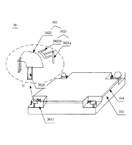
[00731
FIG. 3-1 is a schematic structural diagram of a wireless transceiver apparatus
30
according to an embodiment of the present invention. As shown in FIG. 3-1, the
wireless
transceiver apparatus 30 may include a metal carrier 301 and at least one
antenna unit 302.
[0074] A
groove 3011 is disposed on the metal carrier 301. The groove 3011 may be
disposed
on an edge of the metal carrier 301. Optionally, the groove 3011 may be
located on a corner of the
metal carrier 301, or on a side of the metal carrier 301. The antenna unit 302
is disposed in the
groove 3011 (In this embodiment of the present invention, that the antenna
unit is disposed in the
groove means that all or a part of the antenna unit is disposed in the groove,
and generally, an
orthographic projection of the antenna unit on a bottom surface of the groove
is located in the
8
CA 3031998 2019-04-03
groove). As shown in a dashed box U in FIG. 3-1, in the dashed box U, there is
an enlarged view of
an antenna unit 302 disposed on an edge of the metal carrier 301. The antenna
unit 302 includes a
feeding structure 3021 and a radiation patch 3022. The radiation patch 3022 is
fed by using the
feeding structure 3021, and the radiation patch 3022 is grounded. It should be
noted that the metal
carrier in this embodiment of the present invention may have multiple
structures. The metal carrier
can be used as a reference ground of the antenna unit, and the metal carrier
may be a metal housing
of the wireless transceiver apparatus, a circuit board (for example, a
dielectric substrate), a heat sink,
or the like.
[0075] In actual application, electromagnetic oscillation (also referred
to as resonance) can be
generated between the radiation patch 3022 and a bottom surface of the groove.
Generally, a
capacitance and an inductance are generated between the radiation patch and
the bottom surface of
the groove, and electromagnetic oscillation is excited by the capacitance and
the inductance.
[0076] Optionally, at least one groove 3011 is disposed on the metal
carrier, and one antenna
unit 302 is disposed in each groove 3011. That is, grooves and antenna units
may be disposed in a
one-to-one correspondence, and a quantity of the grooves is equal to a
quantity of the antenna units.
As shown in FIG. 3-1, four grooves 3011 are disposed in FIG. 3-1.
Correspondingly, one antenna
unit 302 is disposed in each groove 3011; that is, there are four antenna
units 302. When at least two
grooves are disposed on the metal carrier, structures of antenna units
disposed in the at least two
grooves may be the same, or may be different. This is not limited in this
embodiment of the present
invention.
00771 According to the wireless transceiver apparatus provided in this
embodiment of the
present invention, an antenna unit is disposed in a groove of a metal carrier,
so that a total thickness
of the wireless transceiver apparatus is reduced, and a total volume is
reduced, thereby reducing
space occupied by the wireless transceiver apparatus.
100781 Further, as shown in FIG. 3-2, the antenna unit 302 may further
include a dielectric
substrate 3023. FIG. 3-2 may be considered as a schematic structural diagram
obtained after a
dielectric substrate is added to the antenna unit that is shown in the dashed
box U in FIG 3-1.
Optionally, the dielectric substrate may be an epoxy resin plate FR-4, and a
dielectric constant of
the epoxy resin plate FR-4 is 4.2; or the dielectric substrate may be made
from another material.
100791 The dielectric substrate 3023 is disposed in the groove 3011, and is
configured to bear
the radiation patch 3022 and the feeding structure 3021; that is, the
radiation patch 3022 is disposed
on the dielectric substrate 3023. Electromagnetic oscillation can be generated
between the radiation
patch 3022 and a bottom surface of the groove 3011. In actual application, the
radiation patch 3022
is laminated on a surface W of the dielectric substrate 3023 (that is, either
of two surfaces of the
9
CA 3031998 2019-04-03
dielectric substrate 3023 that have the largest surface area). A surface of
the radiation patch is
parallel to a surface Q on which the antenna unit 302 is disposed, and a
capacitance may be
generated between the two parallel surfaces. All or a part of the feeding
structure 3021 may be
disposed on the dielectric substrate 3023.
[0080] Optionally, a dielectric substrate (also referred to as a radio
frequency board) 303 may
be further disposed on the metal carrier 301, and the dielectric substrate
3023 of the antenna unit
302 and the dielectric substrate 303 on the metal carrier 301 may be an
integrated structure.
[0081] It may be learned from the foregoing that, according to the
wireless transceiver
apparatus provided in this embodiment of the present invention, a radiation
patch is fed by using a
feeding structure of an antenna unit to implement a feature of the antenna
unit, and the radiation
patch and the feeding structure are further disposed on a dielectric
substrate. When the dielectric
substrate and a dielectric substrate on a metal carrier are an integrated
structure, the antenna unit
does not need to be separately processed or installed, so that complexity of a
manufacturing process
of the wireless transceiver apparatus is reduced, and assembly costs are
reduced. Further, the
.. radiation patch and the feeding structure of the antenna unit are similar
to a planar structure.
Therefore, compared with a three-dimensional structure in the related art, a
total volume of the
antenna unit is reduced, thereby reducing space occupied by the wireless
transceiver apparatus.
[0082] In actual application, the feeding structure may feed the
radiation patch in multiple
manners, such as direct-connection feeding or coupling feeding. When the
feeding structure is in
direct contact with the radiation patch, the feeding structure performs direct-
connection feeding on
the radiation patch. In this feeding manner, an antenna unit can obtain a
relatively low standing
wave bandwidth, and an implementation is simple. However, a bandwidth of the
antenna unit can
be extended by means of coupling feeding.
[0083] For a conventional omnidirectional antenna unit, for example, the
omnidirectional
antenna unit 10 shown in FIG. 1, because of a structure of the omnidirectional
antenna unit, when
multiple antenna units are arranged on the wireless transceiver apparatus, or
when the metal carrier
is asymmetric, relatively high antenna pattern roundness can be maintained in
only a narrowband
range, and relatively low antenna pattern roundness is maintained in a
wideband range. A directivity
pattern is short for an antenna unit directivity pattern, and refers to a
pattern that shows how relative
field strengths (normalized modulus values) in a radiation field change with
directions at a distance
from the antenna unit. Changes of the radiation field are usually represented
by using directivity
patterns of two mutually perpendicular planes in a direction that has highest
radiation power and
that is of the antenna unit. The antenna unit directivity pattern is an
important pattern for measuring
performance of the antenna unit, and parameters of the antenna unit may be
observed from the
CA 3031998 2019-04-03
antenna unit directivity pattern. The antenna pattern roundness (antenna
pattern roundness) is also
referred to as antenna pattern non-roundness, and refers to a difference
between a maximum value
and a minimum value of levels (unit: dB) in each direction of the antenna unit
in a horizontal
directivity pattern.
[0084] To enable the antenna unit 302 to obtain a relatively high standing
wave bandwidth, in
this embodiment of the present invention, as shown in FIG. 4-1, a slot m may
exist between the
feeding structure 3021 and the radiation patch 3022. For example, a slot m may
exist between an
orthographic projection of the feeding structure 3021 on a surface of the
radiation patch 3022 and
the radiation patch 3022, or an overlapping region may exist between an
orthographic projection of
the feeding structure 3021 on a surface of the radiation patch 3022 and the
radiation patch 3022, but
the feeding structure 3021 and the radiation patch 3022 are not coplanar or
laminated together, so
that a slot m is generated. The feeding structure 3021 performs coupling
feeding on the radiation
patch 3022 by using the slot m. Further, as shown in FIG. 4-2, the antenna
unit 302 may further
include:
a parasitic structure 3024, where the parasitic structure 3024 is located on a
surface
parallel to a bottom surface of the groove. For example, the parasitic
structure 3024 may be
supported by some support structures, and be disposed on the surface parallel
to the bottom surface
of the groove; or may be directly disposed on a surface of the dielectric
substrate 3023, and the
dielectric substrate is parallel to the bottom surface of the groove. The
parasitic structure 3024 is
grounded. A slot n exists between the radiation patch 3022 and the parasitic
structure 3024, so that
the radiation patch 3022 can perform coupling feeding on the parasitic
structure 3024. When the
parasitic structure performs coupling feeding on the radiation patch,
electromagnetic oscillation
may be generated between the parasitic structure and the bottom surface of the
groove. The parasitic
structure is added to the antenna unit based on the radiation patch.
Electromagnetic oscillation can
be generated between the parasitic structure and the bottom surface of the
groove, and between the
radiation patch and the bottom surface of the groove. An overall resonance
area of the antenna unit
is in positive correlation with a bandwidth of the antenna unit. Therefore,
when the parasitic
structure performs coupling feeding on the radiation patch, a bandwidth of the
antenna unit can be
further extended while ensuring a relatively small volume of the antenna unit.
[0085] Optionally, as shown in FIG. 4-2 or FIG. 5, the antenna unit 302 may
further include:
a first ground pin 3025, where one end of the first ground pin 3025 is
connected to the
parasitic structure 3024, the other end of the first ground pin 3025 is
connected to the metal carrier
301, the first ground pin 3025 is perpendicular to the bottom, surface Q of
the groove, and the
parasitic structure 3024 is grounded by using the metal carrier 301. The
parasitic structure may be
11
CA 3031998 2019-04-03
disposed parallel to the bottom surface of the groove, so that a capacitance
is generated between the
parasitic structure and the bottom surface of the groove; and then the first
ground pin is disposed, so
that an inductance is generated between the parasitic structure and the bottom
surface of the groove,
and then electromagnetic oscillation is excited. In addition, the first ground
pin not only enables the
__ parasitic structure to be electrically connected to the metal carrier
across a relatively short path, but
also can support the dielectric substrate to avoid deformation of the
dielectric substrate. A
manufacturing technology of the first ground pin is relatively simple.
[0086] In this embodiment of the present invention, the parasitic
structure may feed the
radiation patch in multiple manners, such as direct-connection feeding or
coupling feeding. A
bandwidth of the antenna unit can be extended in the two feeding manners. As
shown in FIG. 5, in
HG. 5, the radiation patch 3022 is in direct contact with the parasitic
structure 3024, and the
radiation patch 3022 performs direct-connection feeding on the parasitic
structure 3024. Optionally,
when the radiation patch 3002 is fed in this manner, a ground cable on a side
is not required, and the
radiation patch 3002 is directly grounded by using the first ground pin 3025
that is connected to the
parasitic structure. In addition, by using the first ground pin, a relatively
strong inductance may be
generated between the radiation patch and the bottom surface of the groove, so
as to ensure that
electromagnetic oscillation is generated between the radiation patch and the
bottom surface of the
groove.
[0087] As shown in FIG. 4-2, a slot n may exist between the parasitic
structure 3024 and the
radiation patch 3022. For example, a slot n exists between an orthographic
projection of the
parasitic structure 3024 on a surface of the radiation patch 3022 and the
radiation patch 3022, or an
overlapping region may exist between an orthographic projection of the
parasitic structure 3024 on
a surface of the radiation patch 3022 and the radiation patch 3022, but the
parasitic structure 3024
and the radiation patch 3022 are not coplanar or laminated together, so that a
slot n is generated.
The parasitic structure 3024 performs coupling feeding on the radiation patch
3022 by using the slot
n. In the coupling feeding manner, the antenna unit 302 may obtain a
relatively high standing wave
bandwidth. It should be noted that when the parasitic structure 3024 performs
coupling feeding on
the radiation patch 3022, the parasitic structure 3024 and the radiation patch
3022 are not in contact
with each other. Therefore, the radiation patch 3022 cannot be grounded by
using the parasitic
structure 3024, and needs to be grounded by using a ground cable or a ground
pin.
[0088] It should be noted that because of performance of the parasitic
structure, for the parasitic
structure, an area required in direct-connection feeding manner is greater
than an area required in a
coupling feeding manner. To reduce a total volume of the antenna unit, the
parasitic structure and
the radiation patch are usually fed in a coupling feeding manner.
12
CA 3031998 2019-04-03
[0089] Further, shapes of the parasitic structure 3024 and the radiation
patch 3022 may match
each other, so as to ensure that the parasitic structure 3024 effectively
feeds the radiation patch 3022.
For example, in the antenna unit 302, when the parasitic structure 3024 feeds
the radiation patch
3022 in a coupling feeding manner, the parasitic structure 3024 and the
radiation patch 3022 may
match each other, so as to ensure that an appropriate slot exists between the
parasitic structure 3024
and the radiation patch 3022. For example, as shown in FIG. 4-2, the parasitic
structure 3024 is a
sector structure, the radiation patch 3022 is a semi-annular structure, and a
center of the radiation
patch 3022 and a center of the parasitic structure 3024 are located on a same
side of the radiation
patch 3022. Optionally, the two centers are close to a corner on which the
antenna unit is disposed,
so that an overall size of the antenna unit can be reduced. It should be noted
that a radiation patch in
an antenna unit on which no parasitic structure is disposed may also be a semi-
annular structure or
another non-centrosymmetric structure. This is not limited in this embodiment
of the present
invention. As shown in FIG. 6, the parasitic structure 3024 is a triangular
structure, the radiation
patch 3022 is a polygonal structure, and two sides that are of the radiation
patch 3022 and the
parasitic structure 3024 and that are close to each other are parallel. For
another example, in the
antenna unit 302, when the parasitic structure 3024 feeds the radiation patch
3022 in a
direct-connection feeding manner, shapes of the parasitic structure 3024 and
the radiation patch
3022 may match each other, so as to ensure an effective connection between the
parasitic structure
3024 and the radiation patch 3022. For example, as shown in FIG 5, the
parasitic structure 3024 is a
sector structure, the radiation patch 3022 is a semi-annular structure, and a
center of the radiation
patch 3022 and a center of the parasitic structure 3024 are located on a same
side of the radiation
patch 3022. An outer edge of the sector structure overlaps an inner edge of
the semi-annular
structure. In FIG 5, the parasitic structure 3024 and the radiation patch 3022
may be located on a
same surface of the dielectric substrate; the parasitic structure 3024
partially overlaps the radiation
patch 3022; and the parasitic structure 3024 and the radiation patch 3022 are
electrically connected
based on contact of the overlapping part. For example, the parasitic structure
3024 and the radiation
patch 3022 may be located on a lower surface of the dielectric substrate, and
an upper surface of the
parasitic structure 3024 partially overlaps a lower surface of the radiation
patch 3022.
[0090] It should be noted that, for the shapes of the parasitic structure
3024 and the radiation
patch 3022, there may be another matching situation. This embodiment of the
present invention is
used only as an example for description. Any modification, equivalent
replacement, or improvement
made based on the matching situation provided in the present invention shall
fall within the
protection scope of the present invention. Therefore, details are not
described in this embodiment of
the present invention.
13
CA 3031998 2019-04-03
[0091] Further, the shapes of the feeding structure 3021 and the
radiation patch 3022 may match
each other, so as to ensure that the feeding structure 3021 effectively feeds
the radiation patch 3022.
In this embodiment of the present invention, the following three possible
implementations are used
as examples for description.
[0092] In a first possible implementation, as shown in any one of FIG. 4-1
to FIG. 5, the feeding
structure 3021 is an E-shaped structure, the E-shaped structure is formed by
one first vertical strip
structure and three first horizontal strip structures whose ends on one side
are disposed on the first
vertical strip structure at intervals, an opening of the E-shaped structure is
disposed opposite to the
radiation patch, a length of a first horizontal strip structure located in the
middle of the E-shaped
structure is greater than a length of each of the other two first horizontal
strip structures, the other
end of the first horizontal strip structure located in the middle of the E-
shaped structure is connected
to a feed of the metal carrier, and the slot is formed between the first
vertical strip structure and the
radiation patch 3022.
[0093] In a second possible implementation, as shown in FIG. 6, the
feeding structure 3021 is a
T-shaped structure, the T-shaped structure is formed by a second vertical
strip structure and one
second horizontal strip structure whose one end extends from a middle part of
the second vertical
strip structure, the other end of the second horizontal strip structure is
connected to a feed of the
metal carrier, and the slot is formed between the second vertical strip
structure and the radiation
patch 3022.
[0094] In a third possible implementation, alternatively, as shown in FIG.
7, the feeding
structure 3021 may be an integrated structure formed by an arc-shaped
structure 30211 and a strip
structure 30212, one end of the strip structure 30212 is connected to a feed
of the metal carrier, and
the other end of the strip structure 30212 is connected to the arc-shaped
structure 30211, an
arc-shaped opening is disposed on a side that is of the radiation patch 3022
and that is close to the
feeding structure 3021, the arc-shaped structure 30211 matches the arc-shaped
opening, the
arc-shaped structure 30211 is located in the arc-shaped opening, and the slot
used for coupling
feeding is formed between the arc-shaped structure 30211 and the arc-shaped
opening.
[0095] It should be noted that, for the shapes of the feeding structure
3021 and the radiation
patch 3022, there may be another matching situation. This embodiment of the
present invention is
used only as an example for description. Any modification, equivalent
replacement, or improvement
made based on the matching situation provided in the present invention shall
fall within the
protection scope of the present invention. Therefore, details are not
described in this embodiment of
the present invention.
[0096] Generally, for a structure of the wireless transceiver apparatus,
three types of symmetry
14
CA 3031998 2019-04-03
relate to roundness: symmetry of an antenna unit, symmetry of an installation
position, and
symmetry of a metal carrier. If the three types of symmetry are all met, that
is, a centrosymmetric
omnidirectional antenna unit is centrosymmetrically disposed on a
centrosymmetric metal carrier,
roundness of the wireless transceiver apparatus is generally relatively high.
If one of the three types
of symmetry is destroyed, roundness generally becomes lower.
[0097] If an omnidirectional antenna unit is installed on a conventional
wireless transceiver
apparatus, generally, the omnidirectional antenna unit is disposed on a
central position of a metal
carrier (the metal carrier is equivalent to a reference ground, that is, a
ground shown in FIG. 8). For
example, the omnidirectional antenna unit is centrosymmetrically disposed on a
shielding cover of
the wireless transceiver apparatus, and a radiation patch or a radiator of the
antenna unit is designed
as a centrosymmetric (also referred to as rotationally symmetric) structure.
In addition, the antenna
unit with a centrosymmetric structure further needs to be placed in the middle
of the metal carrier
(for example, a ground shown in FIG. 8), so that the antenna unit has similar
radiation features on a
cross section parallel to the shielding cover based on structure symmetry,
thereby achieving high
roundness performance. A schematic diagram of corresponding current
distribution is shown in FIG
8. Ground currents of the antenna unit are centrosymmetrically distributed.
However, to implement
multiband coverage and multichannel signal transmission, generally, at least
two omnidirectional
antenna units need to be installed on the wireless transceiver apparatus. In
this case, when there are
multiple antenna units, because it cannot be ensured that a metal carrier is
symmetric relative to
each antenna unit, non-centrosymmetric distribution of ground currents is
inevitably caused, and
antenna pattern roundness becomes lower. In actual application, because of
processing convenience,
the metal carrier is a centrosymmetric structure, for example, a square
structure or a circular
structure, and a shielding cover buckled on the metal carrier is also a
centrosymmetric structure.
Optionally, the metal carrier may be a centrosymmetric prismatic structure.
For beauty, an edge of
the metal carrier may be rounded or beveled.
[0098] FIG. 9 is a schematic diagram of current distribution of an
antenna unit in a scenario that
is shown in FIG. 2 and in which omnidirectional antenna units are disposed on
four corners of a
shielding cover. A metal carrier is used as a reference ground (a ground shown
in FIG. 9) of the
antenna unit, and the metal carrier is not centrosymmetric relative to each
antenna unit, and
consequently, ground currents of each antenna unit are non-centrosymmetrically
distributed.
Correspondingly, an emulation diagram of a directivity pattern of the antenna
unit may be shown in
FIG. 10. Antenna pattern roundness corresponding to different frequencies in
FIG. 10 is shown in
Table 1. A cross section of a three-dimension directivity pattern at an angle
Theta in a horizontal
plane direction is obtained. A value range of Theta is usually 0 to 180 , and
a frequency value
CA 3031998 2019-04-03
recorded in Table 1 is a frequency value corresponding to a frequency required
when the antenna
unit is normally working. Theta cross section roundness represents a
difference between a
maximum value and a minimum value of levels (unit: dB) in a directivity
pattern obtained when an
angle is Theta. In addition, for the sake of a coverage area, a cross section
of Theta=80 is usually
considered. Theta=80 represents that an included angle between a radiation
direction and a vertical
direction in a polar coordinate system is 800. It may be learned from the
emulation diagram shown
in FIG. 10 and Table 1, when conventional wideband monopole antenna units are
arranged on four
corners of a metal carrier, because an antenna unit is non-centrosymmetrically
distributed for the
metal carrier, and consequently, ground currents of the metal carrier are non-
centrosymmetrically
distributed. Therefore, a relatively deep pit of a directivity pattern is
formed in an opposite angle
direction of the metal carrier, antenna pattern roundness becomes extremely
low, and the lowest
roundness in a wideband range of 1.7 GHz to 2.7 GHz (GHz) is 10.9 dB (dB). A
fluctuation degree
of the directivity pattern far exceeds a fluctuation range that is acceptable
to a communications
operator. A huge fluctuation in a horizontal cross section directivity pattern
will lead to a
communications dead zone, and consequently, a coverage area is reduced, and a
communication
capability is reduced.
Table 1
Frequency (GHz) Cross section roundness (dB) when Theta=80
1.7 4.2
1.9 5.8
2.1 7.6
2.3 9.7
2.5 10.9
2.7 8.9
[0099] In this embodiment of the present invention, to implement
multiband coverage and
multichannel signal transmission, generally, at least two omnidirectional
antenna units need to be
installed on the wireless transceiver apparatus. As shown in any one of FIG 3-
1 to FIG. 7, the
radiation patch 3022 and the feeding structure 3021 in each antenna unit on
the wireless transceiver
apparatus in this embodiment of the present invention may be non-
centrosymmetric structures. The
radiation patch 3022 and the feeding structure 3021 in each antenna unit in
this embodiment of the
present invention may be non-centrosymmetric structures, the metal carrier is
used as a reference
ground of the antenna unit, and the metal carrier is non-centrosymmetric
relative to each antenna
16
CA 3031998 2019-04-03
unit. Therefore, for each antenna unit, ground currents generated by a non-
centrosymmetric
radiation patch and a non-centrosymmetric reference ground may be relatively
centrosymmetrically
distributed. Compared with the omnidirectional antenna unit in the
conventional wireless
transceiver apparatus, each antenna unit in the wireless transceiver apparatus
provided in this
embodiment of the present invention has relatively high roundness in a
wideband range. In addition,
the parasitic structure may be a non-centrosymmetric structure, so as to
further ensure antenna
pattern roundness of the antenna unit.
[0100] In actual application, relative positions of the radiation patch,
the feeding structure, and
the parasitic structure on the dielectric substrate may be determined
according to a specific situation.
Two of the radiation patch, the feeding structure, and the parasitic structure
may be located on one
side of the dielectric substrate, and one of the radiation patch, the feeding
structure, and the parasitic
structure may be located on the other side of the dielectric substrate; or the
radiation patch, the
feeding structure, and the parasitic structure are located on a same side of
the dielectric substrate. As
shown in FIG. 4-2, FIG 6, or FIG. 7, the radiation patch 3022 and the feeding
structure 3021 are
located on one side of the dielectric substrate, and the parasitic structure
3024 is located on the other
side of the dielectric substrate. As shown in FIG. 5 or FIG. 11, the radiation
patch 3022 and the
parasitic structure 3024 are located on one side of the dielectric substrate
3023, and the feeding
structure 3021 is located on the other side of the dielectric substrate 3023.
For example, the
radiation patch and the parasitic structure are located on a lower surface of
the dielectric substrate,
and the feeding structure is located on an upper surface of the dielectric
substrate.
[0101] Certainly, when no parasitic structure is disposed on the wireless
transceiver apparatus,
relative positions of the radiation patch 3022 and the feeding structure 3021
on the dielectric
substrate may be determined according to a specific situation. The radiation
patch 3022 and the
feeding structure 3021 may be respectively located on two sides of the
dielectric substrate 3023, or
the radiation patch 3022 and the feeding structure 3021 may be located on a
same side of the
dielectric substrate 3023. As shown in FIG. 3-2, the radiation patch 3022 and
the feeding structure
3021 are located on a same side of the dielectric substrate 3023. As shown in
FIG. 12, the radiation
patch and the feeding structure are respectively located on two sides of the
dielectric substrate.
[0102] In FIG 12, the radiation patch 3022 is located on a lower surface
of the dielectric
substrate 3023. The antenna unit 302 may further include: a second ground pin
3026 disposed on at
least one side of the radiation patch 3022. The second ground pin 3026 may be
made of metal. One
end of the second ground pin 3026 is connected to the radiation patch 3022,
and the other end of the
second ground pin 3026 is connected to the metal carrier 301. The second
ground pin 3026 is
perpendicular to a surface of the dielectric substrate 3023, and the radiation
patch 3022 is grounded
17
CA 3031998 2019-04-03
by using the metal carrier 301. For example, in FIG 12, two second ground pins
3026 are disposed
in the antenna unit 302. The two second ground pins 3026 are symmetrically
disposed on two sides
of the radiation patch 3022. Based on the second ground pin 3026, the
radiation patch may be
disposed parallel to a bottom surface of the groove, so that a capacitance is
generated between the
radiation patch and the bottom surface of the groove; and then the second
ground pin is disposed, so
that an inductance is generated between the radiation patch and the bottom
surface of the groove,
and then electromagnetic oscillation is excited. In addition, the second
ground pin not only enables
the radiation patch to be electrically connected to the metal carrier across a
relatively short path, but
also can support the dielectric substrate to avoid deformation of the
dielectric substrate. A
manufacturing technology of the second ground pin is relatively simple. In
addition, two second
ground pins 3026 are symmetrically disposed on two sides of the radiation
patch 3022, so that a size
of the antenna unit can be effectively reduced, and a bandwidth is extended.
[0103] As shown in any one of FIG 4-1 to FIG. 7, or as shown in FIG. 11
or FIG 12, the
wireless transceiver apparatus 30 may further include a shielding cover 304.
The shielding cover
.. 304 is buckled on the dielectric substrate 303 of the metal carrier 301,
and is configured to shield
interference between a radio frequency circuit and an external environment and
interference
between the radio frequency circuit and an antenna unit. It should be noted
that a shape of the
shielding cover may be adaptively adjusted according to positions of grooves
on the metal carrier.
For example, when the grooves are located on four corners of the metal
carrier, grooves that match
the grooves are also disposed on four corners of the shielding cover, so that
the grooves of the
shielding cover and the metal carrier are connected, and the shielding cover
and the metal carrier
are effectively buckled.
[0104] In actual application, alternatively, the wireless transceiver
apparatus 30 may be shown
in FIG. 13, and does not include the shielding cover. The dielectric substrate
is directly buckled on
.. the metal carrier (in actual application, the dielectric substrate may also
be disposed inside the metal
carrier, and FIG. 13 is used only as an example for description). Optionally,
for a component that is
inside the metal carrier and for which a shielding structure needs to be
disposed, a small shielding
cover may be buckled outside the component to avoid interference between the
component and an
external environment. As shown in FIG. 13, no shielding cover is disposed on
the wireless
.. transceiver apparatus 30, so that a total thickness of the wireless
transceiver apparatus may be
reduced, and correspondingly, a volume of the wireless transceiver apparatus
is reduced.
[0105] It should be noted that, alternatively, the radiation patch 3022
may be grounded in
another manner in addition to using the ground pin. Optionally, as shown in
FIG. 4-1 or FIG. 4-2,
the antenna unit 302 may further include:
18
CA 3031998 2019-04-03
a ground cable 3027, where the ground cable 3027 is made of metal, one end of
the
ground cable 3027 is connected to the radiation patch 3022, and the other end
of the ground cable
3027 is connected to a metal ground cable (not shown in the figure) of the
dielectric substrate 3023,
so that the radiation patch 3022 is grounded by using the metal ground cable
(not shown in the
figure). For an antenna unit on which the ground cable is disposed, a weak
inductance may be
generated between the radiation patch and a bottom surface of the groove, so
that electromagnetic
oscillation is generated between the radiation patch and the bottom surface of
the groove. In this
embodiment of the present invention, to ensure that a relatively strong
inductance is generated
between the radiation patch and the bottom surface of the groove, when the
radiation patch is
grounded by using the ground cable, a ground pin perpendicular to the bottom
surface of the groove
may be added below the radiation patch; or when the radiation patch is
grounded by using the
ground cable, a parasitic structure may be added, and a ground pin
perpendicular to the bottom
surface of the groove may be added below the parasitic structure. In this way,
a relatively strong
inductance is generated. In actual application, alternatively, the inductance
may be increased in
another manner. This is not limited in this embodiment of the present
invention.
[0106] A quantity of ground cables 3027 in the antenna unit 302 may be
determined according
to an actual situation. For example, as shown in FIG. 6, the ground cable 3027
is disposed on a side
of the radiation patch 3022, and the feeding structure 3021 is disposed on
another side of the
radiation patch.
[0107] For another example, as shown in FIG. 4-1, there are two ground
cables 3027 in total.
The two ground cables 3027 are symmetrically disposed on two sides of the
radiation patch 3022,
and are separately connected to the metal ground cable of the dielectric
substrate 3023. The feeding
structure 3021 is an axisymmetric structure, and a symmetry axis of the
feeding structure 3021 is
the same as a symmetry axis of the two ground cables 3027. In this way,
antenna pattern roundness
may be relatively easily controlled.
[0108] Further, as shown in any one of FIG. 3-1 to FIG. 7 or FIG. 11 to
FIG. 13, an opening may
exist on a side wall of the groove, that is, the side wall of the groove is
non-closed. In FIG. 3-1 to
FIG. 7, the groove is disposed on a corner of the metal carrier, and an
opening of the two adjacent
side walls of the groove. When the groove is disposed on a side of the metal
carrier, an opening may
exist on a side wall. In this way, effective feeding and energy radiation of
the antenna unit can be
ensured. In addition, a half-open groove can be easily processed,
manufactured, and assembled.
[0109] Optionally, a heat sink fin may be further disposed on a bottom of
the metal carrier. The
heat sink fin is configured to dissipate heat for the metal carrier.
[0110] For the omnidirectional antenna unit in the wireless transceiver
apparatus in any one of
19
CA 3031998 2019-04-03
FIG. 3-1 to FIG. 7 or FIG. 11 to FIG. 13 in the present invention, a voltage
standing wave ratio
(English: Voltage Standing Wave Ratio, VSWR for short) may be less than 2.5,
and a standing wave
bandwidth may be greater than 45%.
[0111] For the wireless transceiver apparatus 30 shown in FIG. 4-2, a
left view and a top view
of the wireless transceiver apparatus 30 are respectively shown in FIG. 14 and
FIG. 15. FIG. 14 and
FIG. 15 show structure parameters of the wireless transceiver apparatus 30. As
shown in FIG. 14, a
thickness of the wireless transceiver apparatus 30 is hO, that is, a total
thickness of the metal carrier
301, the dielectric substrate 3023 (or the dielectric substrate 303), and the
shielding cover 304 that
are sequentially superposed from bottom to top is h0. A depth of the groove
3011 is hl¨h3, and h3
is a thickness of the shielding cover. A distance from a lower surface of the
dielectric substrate 3023
to a bottom surface of the groove 3011 is h. A height of the first ground pin
3025 is h2. The
dielectric substrate 303 and the groove 3011 have a same shape, and may have a
same size or
different sizes. Generally, a size of the dielectric substrate 303 is less
than a size of the groove 3011.
As shown in FIG. 15, a top view of the groove 3011 is a square that has a
corner from which an
isosceles right triangle is cut off. A side length of the square is cO, and a
side length of the isosceles
right triangle is c0¨c1. Distances from a center of a sector (which may also
be considered as a
quarter of a circle) parasitic structure 3024 to two sides of the groove 3011
are both rO, a radius of
the sector is rl, and a central angle corresponding to the sector is 90 . For
a semi-annular (which
may also be considered as a quarter of a ring) radiation patch 3022, an inner
diameter is r2, an outer
diameter is r3, and a central angle is 900. A center of the radiation patch
coincides with the center of
the sector parasitic structure. The radiation patch 3022 is an E-shaped
structure, and a first vertical
strip structure of the radiation patch 3022 is a semi-annular structure. For
the semi-annular structure,
an inner diameter is r4, an outer diameter is r5, and a central angle is a. A
first horizontal strip
structure located on an external edge of the E-shaped structure has a length
of la and a width of wa.
A first horizontal strip structure located in the middle of the E-shaped
structure has a length of If
and a width of wf. There are two ground cables 3027. The two ground cables
3027 are
symmetrically disposed on two sides of the radiation patch 3022, and are
separately connected to
the metal ground cable of the dielectric substrate 3023. Each ground cable
3027 is a strip structure,
and has a length of ws and a width of Is.
[0112] For example, values of structure parameters of the antenna unit in
the wireless
transceiver apparatus 30 shown in FIG 4-2 are shown in Table 2. kl is a
wavelength corresponding
to a lowest operating frequency of the antenna unit in the wireless
transceiver apparatus 30, and r0
(0.05104k1, 0.07656k1) represents that 1.0 is in a range of 0.051042J to
0.07656k1.
CA 3031998 2019-04-03
Table 2
Structure parameter Value Structure parameter Value
0.0593X1 r4 (0.1216X1, 0.1824X1)
h0 0.1712J r5 (0.1336M, 0.2004M)
hl 0.12021 wa 0.0126X1
h2 0.0483M ws 0.0105X1
c0 0.251X1 wf 0.0188X1
cl 0.145X1 la 0.0436X1
r0 (0.05104M, 0.07656M) ls 0.039121
rl (0.05472M, 0.08208X1) If 0.0377X1
r2 (0.0848k1, 0.1776X1) a 25.7
r3 (0.1184M. 0.1776k1)
[0113] When the values of the structure parameters of the antenna unit in
the wireless
transceiver apparatus 30 in FIG. 4-2 are shown in Table 2, for an antenna unit
designed according to
the structure parameters in Table 2, an emulation diagram of a directivity
pattern of the antenna unit
obtained by means of emulation may be shown in FIG. 16. When Theta=80 ,
antenna pattern
roundness corresponding to different frequencies in FIG. 16 is shown in Table
3. It can be learned
from the emulation diagram shown in FIG. 16 and Table 3 that the antenna unit
with this structure
form in the wireless transceiver apparatus 30 shown in FIG 4-2 has a lowest
roundness of 3.3 dB in
a frequency band range of 1.7 GHz to 2.7 GHz. The directivity pattern has a
relatively low
fluctuation, so that a relatively large coverage area can be provided, and a
communications
capability is improved.
Table 3
Frequency (GHz) Cross section roundness (dB) when Theta=80
1.7 3.3
1.9 3.3
2.1 2.3
2.3 2.5
2.5 2.6
2.7 3.1
[0114] For the wireless transceiver apparatus 30 shown in FIG. 13, a left
view and a top view of
21
CA 3031998 2019-04-03
the wireless transceiver apparatus 30 are respectively shown in FIG. 17 and
FIG. 18. FIG. 17 and
FIG. 18 show structure parameters of the wireless transceiver apparatus 30. As
shown in FIG. 17, a
thickness of the wireless transceiver apparatus 30 is hO, that is, a total
thickness of the metal carrier
301 and the dielectric substrate 3023 (or the dielectric substrate 303) that
are sequentially
superposed from bottom to top is h0. A depth of the groove 3011 is hi. A
distance from a lower
surface of the dielectric substrate 3023 to a bottom surface of the groove
3011 is h. A height of the
first ground pin 3025 is h2. As shown in FIG. 18, a top view of the groove
3011 (The dielectric
substrate and the groove have a same shape) is a square that has a corner from
which an isosceles
right triangle is cut off. A side length of the square is cO, and a side
length of the isosceles right
triangle is c0¨el. Distances from a center of a sector (which may also be
considered as a quarter of
a circle) parasitic structure 3024 to two sides of the groove 3011 are both
rO, a radius of the sector is
rl, and a central angle is 90 . A center of the radiation patch coincides with
the center of the sector
parasitic structure. The radiation patch 3022 is an E-shaped structure, and a
first vertical strip
structure of the radiation patch 3022 is a semi-annular structure. For the
semi-annular structure, an
inner diameter is r4, an outer diameter is r5, and a central angle is a. A
first horizontal strip structure
located on an external edge of the E-shaped structure has a length of la and a
width of wa. A first
horizontal strip structure located in the middle of the E-shaped structure has
a length of If and a
width of wf. There are two ground cables 3027. The two ground cables 3027 are
symmetrically
disposed on two sides of the radiation patch 3022, and are separately
connected to the metal ground
cable of the dielectric substrate 3023. Each ground cable 3027 is a strip
structure, and has a length
of ws and a width of Is.
[0115] Values of structure parameters of the antenna unit in the wireless
transceiver apparatus
shown in FIG. 13 are shown in Table 4. XI is a wavelength corresponding to a
lowest operating
frequency of the antenna unit in the wireless transceiver apparatus 30, and r0
(0.0328k1, 0.0492k1)
25 represents that r0 is in a range of 0.0328k1 to 0.0492k1.
Table 4
Structure parameter Value Structure parameter Value
0.0593k1 r4 (0.1272k1, 0.1908k1)
h0 0.120k1 r5 (0.1376k1, 0.2064k1)
h2 0.0483k1 wa 0.008X1
c0 0.274k1 ws 0.008X1
e 1 0.188k1 wf 0.0148X1
r0 (0.0328k1, 0.0492X1) la 0.0444k1
22
CA 3031998 2019-04-03
rl (0.06211, 0.09311) Is 0.0313k1
r2 (0.0962.1, 0.1442.1) If 0.0319k1
r3 (0.12484 0.18722.1) a 26.89'
101161 When the values of the structure parameters of the antenna unit in
the wireless
transceiver apparatus 30 in FIG. 13 are shown in Table 4, an emulation diagram
of a directivity
pattern of the antenna unit may be shown in FIG. 19. When Theta=80 , antenna
pattern roundness
corresponding to different frequencies in FIG 19 is shown in Table 5. It can
be learned from the
emulation diagram shown in FIG 19 and Table 5 that the antenna unit in the
wireless transceiver
apparatus 30 shown in FIG. 13 has a lowest roundness of 5.4 dB in a frequency
band range of 1.7
GHz to 2.7 GHz. The directivity pattern has a relatively low fluctuation, so
that a relatively large
coverage area can be provided, and a communications capability is improved.
Table 5
Frequency (GHz) Cross section roundness (dB) when Theta=80
1.7 5.1
1.9 5.4
2.1 4.4
2.3 3.2
2.5 3.4
2.7 3.2
10117] For the wireless transceiver apparatus 30 shown in FIG. 11, a left
view and a top view of
the wireless transceiver apparatus 30 are respectively basically the same as
the left view and the top
view of the wireless transceiver apparatus 30 in FIG. 13, but the radiation
patch 3022 cannot be
directly seen from the top view of the wireless transceiver apparatus 30 in
FIG. 11. For a left view
and a top view of the wireless transceiver apparatus 30 shown in FIG. 11,
refer to FIG. 17 and FIG.
18. As shown in FIG. 17, a thickness of the wireless transceiver apparatus 30
is hO, that is, a total
thickness of the metal carrier 301 and the dielectric substrate 3023 (or the
dielectric substrate 303)
that are sequentially superposed from bottom to top is h0. A depth of the
groove 3011 is hl. A
distance from a lower surface of the dielectric substrate 3023 to a bottom
surface of the groove 3011
is h. A height of the first ground pin 3025 is h2. As shown in FIG. 18, a top
view of the groove 3011
(The dielectric substrate and the groove have a same shape) is a square that
has a corner from which
an isosceles right triangle is cut off. A side length of the square is cO, and
a side length of the
23
CA 3031998 2019-04-03
isosceles right triangle is c0¨el. Distances from a center of a sector (which
may also be considered
as a quarter of a circle) parasitic structure 3024 to two sides of the groove
3011 are both 1.0, a radius
of the sector is rl, and a central angle is 900. For a semi-annular (which may
also be considered as a
quarter of a ring) radiation patch 3022, an inner diameter is r2, an outer
diameter is r3, and a central
angle is 90 . A center of the radiation patch coincides with the center of the
sector parasitic structure.
The radiation patch 3022 is an E-shaped structure, and a first vertical strip
structure of the radiation
patch 3022 is a semi-annular structure. For the semi-annular structure, an
inner diameter is r4, an
outer diameter is r5, and a central angle is a. A first horizontal strip
structure located on an external
edge of the E-shaped structure has a length of la and a width of wa. A first
horizontal strip structure
located in the middle of the E-shaped structure has a length of lf and a width
of wf. There are two
ground cables 3027. The two ground cables 3027 are symmetrically disposed on
two sides of the
radiation patch 3022, and are separately connected to the metal ground cable
of the dielectric
substrate 3023. Each ground cable 3027 is a strip structure, and has a length
of ws and a width of is.
[0118] Values of structure parameters of the antenna unit in the wireless
transceiver apparatus
30 shown in FIG. 11 are shown in Table 6. X1 is a wavelength corresponding to
a lowest operating
frequency of the antenna unit in the wireless transceiver apparatus 30, and r0
(0.05104X1, 0.07656M)
represents that r0 is in a range of 0.05104k1 to 0.07656k1.
Table 6
Structure parameter Value Structure parameter Value
0.0593M r4 (0.12X1, 0.18X1)
h0 0.171X1 r5 (0.1304M, 0.1956X1)
hl 0.120k1 wa 0.0122X1
h2 0.0483M ws 0.009k1
c0 0.251X1 wf 0.02X1
cl 0.145M la 0.045k1
r0 (0.05104M, 0.07656X1) Is 0.0407X1
rl (0.05576M, 0.08364X1) If 0.0414X1
r2 (0.08642J, 0.1296X1) a 28.56deg
r3 (0.1176M. 0.1764k1)
[0119] When the values of the structure parameters of the antenna unit in
the wireless
transceiver apparatus 30 in FIG. 11 are shown in Table 6, an emulation diagram
of a directivity
pattern of the antenna unit may be shown in FIG. 20. When Theta=80 , antenna
pattern roundness
24
CA 3031998 2019-04-03
corresponding to different frequencies in FIG 20 is shown in Table 7. It can
be learned from the
emulation diagram shown in FIG. 20 and Table 7 that the antenna unit in the
wireless transceiver
apparatus 30 shown in FIG. 11 has a lowest roundness of 3.6 dB in a frequency
band range of 1.7
GHz to 2.7 GHz. The directivity pattern has a relatively low fluctuation, so
that a relatively large
coverage area can be provided, and a communications capability is improved.
Table 7
Frequency (GHz) Cross section roundness (dB) when Theta=80
1.7 3.4
1.9 3.6
2.1 2.5
2.3 2.6
2.5 2.9
2.7 3.6
[0120] For the wireless transceiver apparatus 30 shown in FIG. 12, a left
view and a top view of
the wireless transceiver apparatus 30 are respectively shown in FIG. 21 and
FIG. 22. FIG. 21 and
FIG. 22 show structure parameters of the antenna unit in the wireless
transceiver apparatus 30. As
shown in FIG 21, a thickness of the wireless transceiver apparatus 30 is hO,
that is, a total thickness
of the metal carrier 301 and the dielectric substrate 3023 (or the dielectric
substrate 303) that are
sequentially superposed from bottom to top is h0. A depth of the groove 3011
is hl¨h3, and h3 is a
thickness of the shielding cover. A distance from a lower surface of the
dielectric substrate 3023 to a
bottom surface of the groove 3011 is equal to a height of a second ground pin
3026, and is h. A
projection distance from the second ground pin 3026 to the center of the
radiation patch 3022 is ps.
A width of each second ground pin 3026 is ws. As shown in FIG. 22, atop view
of the groove 3011
(The dielectric substrate and the groove have a same shape) is a square that
has a corner from which
an isosceles right triangle is cut off. A side length of the square is cO, and
a side length of the
isosceles right triangle is c0¨cl. For a semi-annular (which may also be
considered as a quarter of a
ring) radiation patch 3022, an inner diameter is rl, an outer diameter is r2,
and a central angle is 90 .
Distances from a center of the semi-annular (which may also be considered as a
quarter of a ring)
radiation patch 3022 to two sides of the groove 3011 are both r0. The
radiation patch 3022 is an
E-shaped structure, and a first vertical strip structure of the radiation
patch 3022 is a semi-annular
structure. For the semi-annular structure, an inner diameter is r4, an outer
diameter is r5, and a
central angle is a. A first horizontal strip structure located on an external
edge of the E-shaped
CA 3031998 2019-04-03
structure has a length of la and a width of wa. A first horizontal strip
structure located in the middle
of the E-shaped structure has a length of If and a width of wf.
[0121] Values of structure parameters of the antenna unit in the wireless
transceiver apparatus
30 shown in FIG. 12 are shown in Table 8. X1 is a wavelength corresponding to
a lowest operating
frequency of the antenna unit in the wireless transceiver apparatus 30, and r0
(0.03736X1, 0.05604X1)
represents that r0 is in a range of 0.03736X1 to 0.05604X1.
Table 8
Structure parameter Value Structure parameter Value
0.0593X1 r4 (0.14X1, 0.122J)
h0 0.171X1 wa 0.0134X1
hl 0.120M ws 0.0378X1
c0 0.262X1 wf 0.0313X1
cl 0.177X1 la 0.0509X1
r0 (0.03736M, 0.05604XI) ps 0.0413X1
rl (0.03688M, 0.055322d) If 0.0704X1
r2 (0.11682J, 0.175221) a 23.4deg
r3 (0.12564 0.1884M)
[0122] When the values of the structure parameters of the antenna unit in
the wireless
transceiver apparatus 30 in FIG. 12 are shown in Table 8, an emulation diagram
of a directivity
pattern of the antenna unit may be shown in FIG. 23. When Theta=80 , antenna
pattern roundness
corresponding to different frequencies in FIG. 23 is shown in Table 9. It can
be learned from the
emulation diagram shown in FIG. 23 and Table 9 that the antenna unit in the
wireless transceiver
apparatus 30 shown in FIG 13 has a lowest roundness of 5.8 dB in a frequency
band range of 1.7
GHz to 2.7 GHz. The directivity pattern has a relatively low fluctuation, so
that a relatively large
coverage area can be provided, and a communications capability is improved.
Table 9
Frequency (GHz) Cross section roundness (dB) when Theta=80
1.7 2.6
1.9 3.1
2.1 4.0
26
CA 3031998 2019-04-03
2.3 4.1
2.5 5.1
2.7 5.8
[0123] For the wireless transceiver apparatus 30 shown in FIG 7, a left
view of the wireless
transceiver apparatus 30 is the same as that shown in FIG. 17. For a top view
of the wireless
transceiver apparatus 30, refer to FIG. 24. As shown in FIG. 17, a thickness
of the wireless
transceiver apparatus 30 is hO, that is, a total thickness of the metal
carrier 301 and the dielectric
substrate 3023 (or the dielectric substrate 303) that are sequentially
superposed from bottom to top
is h0. A depth of the groove 3011 is hl. A distance from a lower surface of
the dielectric substrate
3023 to a bottom surface of the groove 3011 is h. A height of the first ground
pin 3025 is h2. As
shown in FIG. 24, a top view of the groove 3011 (The dielectric substrate and
the groove have a
same shape) is a square that has a corner from which an isosceles right
triangle is cut off. A side
length of the square is cO, and a side length of the isosceles right triangle
is c0¨cl. Distances from a
center of a sector (which may also be considered as a quarter of a circle)
parasitic structure 3024 to
two sides of the groove 3011 are both rO, a radius of the sector is r 1, and a
central angle is 90 . For a
semi-annular (which may also be considered as a quarter of a ring) radiation
patch 3022, an inner
diameter is r2, an outer diameter is r3, and a central angle is 90 . An arc-
shaped opening is disposed
on a side that is of the radiation patch 3022 and that is close to the feeding
structure 3021, and a
radius of the arc-shaped opening is r5. A center of the radiation patch
coincides with the center of
the sector parasitic structure. The feeding structure 3021 is an integrated
structure formed by an
arc-shaped structure 30211 and a strip structure 30212. The strip structure
has a length of wf and a
width of lf. The arc-shaped structure 30211 has a radius r4, and is concentric
with the arc-shaped
opening. There are two ground cables 3027. The two ground cables 3027 are
symmetrically
disposed on two sides of the radiation patch 3022, and are separately
connected to the metal ground
cable of the dielectric substrate 3023. Each ground cable 3027 is a strip
structure, and has a length
of ws and a width of Is.
[0124] Values of structure parameters of the antenna unit in the wireless
transceiver apparatus
shown in FIG. 7 are shown in Table 10. X1 is a wavelength corresponding to a
lowest operating
frequency of the antenna unit in the wireless transceiver apparatus 30, and r0
(0.04564 0.0648k1)
represents that r0 is in a range of 0.0456X1 to 0.0648X1.
Table 10
Structure parameter Value Structure parameter j Value
27
CA 3031998 2019-04-03
0.05932d r2 (0.0896X1, 0.13442J)
h0 0.171X1 r3 (0.1424X1, 0.2136X1)
hl 0.120X1 r4 (0.03128M, 0.04692M)
h2 0.0483X1 r5 (0.04562d, 0.06842])
c0 0.257k1 wf 0.01452.1
cl 0.171X1 ws 0.00312.1
rO (0.04564 0.06482.1) If 0.04312.1
rl (0.054242.1, 0.081362.1) Is 0.02082.1
[0125] When the values of the structure parameters of the antenna unit in
the wireless
transceiver apparatus 30 in FIG 7 are shown in Table 10, an emulation diagram
of a directivity
pattern of the antenna unit may be shown in FIG. 25. When Theta=80 , antenna
pattern roundness
corresponding to different frequencies in FIG 25 is shown in Table 11. It can
be learned from the
emulation diagram shown in FIG. 25 and Table 11 that the antenna unit in the
wireless transceiver
apparatus 30 shown in FIG. 7 has a lowest roundness of 4.6 dB in a frequency
band range of 1.7
GElz to 2.7 GHz. The directivity pattern has a relatively low fluctuation, so
that a relatively large
coverage area can be provided, and a communications capability is improved.
Table!!
Frequency (GHz) Cross section roundness (dB) when Theta=80
1.7 4.1
1.9 4.6
2.1 3.7
2.3 3.2
2.5 3.4
2.7 3.6
[0126] For the wireless transceiver apparatus 30 shown in FIG. 6, a left
view of the wireless
transceiver apparatus 30 is the same as that shown in FIG. 17. For a top view
of the wireless
transceiver apparatus 30, refer to FIG. 26. As shown in FIG. 17, a thickness
of the wireless
transceiver apparatus 30 is hO, that is, a total thickness of the metal
carrier 301 and the dielectric
substrate 3023 (or the dielectric substrate 303) that are sequentially
superposed from bottom to top
is h0. A depth of the groove 3011 is hl. A distance from a lower surface of
the dielectric substrate
3023 to a bottom surface of the groove 3011 is h. A height of the first ground
pin 3025 is h2. As
28
CA 3031998 2019-04-03
shown in FIG. 26, a top view of the groove 3011 (The dielectric substrate and
the groove have a
same shape) is a square that has a corner from which an isosceles right
triangle is cut off. A side
length of the square is cO, and a side length of the isosceles right triangle
is c0¨cl. Distances from a
vertex of an isosceles right triangle parasitic structure 3024 to two sides of
the groove 3011 are both
1-0, and a side length is al. A top view of the radiation patch 3022 is a
square that has two corners
from which isosceles right triangles are respectively cut off. The two corners
are respectively a
corner that is close to the parasitic structure 3024 and a corner that is
close to an end, with a corner
cut off, of the groove. A side that is of the radiation patch 3022 and that is
close to the parasitic
structure 3024 is parallel to a bottom of the parasitic structure 3024. The
remaining sides of the
radiation patch 3022 are parallel to corresponding sides in the top view of
the groove 3011. A side
length of one side of the cut isosceles right triangle is a3, and a side
length of another side of the cut
isosceles right triangle is a4. The feeding structure 3021 is a T-shaped
structure, and a length of a
second vertical strip structure of the feeding structure 3021 is w2. A long
side is parallel to a side
that is of the radiation patch and that has a width of a4, and a distance
between each other is wl. A
second horizontal strip structure of the feeding structure 3021 has a length
of If and a width of wf.
There is one ground cable 3027, and the ground cable 3027 and the feeding
structure 3021 are
located on different sides of the radiation patch 3022. The ground cable 3027
is connected to the
metal ground cable of the dielectric substrate 3023. The ground cable 3027 is
a strip structure, and
has a length of ws and a width of Is.
[0127] Values of structure parameters of the antenna unit in the wireless
transceiver apparatus
shown in FIG. 6 are shown in Table 12. kl is a wavelength corresponding to a
lowest operating
frequency of the antenna unit in the wireless transceiver apparatus 30, and 1-
0 (0.0644k1, 0.0966k1)
represents that r0 is in a range of 0.0644k1 to 0.0966k1.
Table 12
Structure parameter Value Structure parameter Value
0.0793k1 a3 0.0794k1
h0 0.181k1 a4 0.138k1
hl 0.13k1 wl 0.0007k1
h2 0.0593k1 w2 0.0085k1
c0 0 .3 kl wf 0.0226k1
c 1 0.215k1 vs 0.0237k1
rO (0.0644)1 0.0966k1) 11 0.0397AA
al 0.0476k1 If 0.0475k1
29
CA 3031998 2019-04-03
a2 0.0309k1 Is 0.05672J
101281 When the values of the structure parameters of the antenna unit in
the wireless
transceiver apparatus 30 in FIG. 6 are shown in Table 12, an emulation diagram
of a directivity
pattern of the antenna unit may be shown in FIG. 27. When Theta=80 , antenna
pattern roundness
corresponding to different frequencies in FIG 27 is shown in Table 13. It can
be learned from the
emulation diagram shown in FIG. 27 and Table 13 that the antenna unit in the
wireless transceiver
apparatus 30 shown in FIG. 6 has a lowest roundness of 4.4 dB in a frequency
band range of 1.7
GHz to 2.7 GHz. The directivity pattern has a relatively low fluctuation, so
that a relatively large
coverage area can be provided, and a communications capability is improved.
Table 13
Frequency (GHz) Cross section roundness (dB) when Theta=80
1.7 3.2
1.9 3.5
2.1 3.9
2.3 4.3
2.5 4.4
2.7 4.4
[0129] Optionally, alternatively, the antenna unit 30 in the groove 3011
may be shown in FIG.
3-1 or FIG. 3-2. In FIG. 3-2, the feeding structure 3021 is formed by two
feeding sub-structures. A
part is a first feeding sub-structure 3021a that is perpendicular to a bottom
surface of the groove
3011 and that is configured to be connected to a feed on the metal carrier,
and the other part is a
second feeding sub-structure 3021b parallel to the bottom surface of the
groove 3011. In FIG. 3-2,
an example in which the second feeding sub-structure 3021b is printed on an
upper surface of the
dielectric substrate 3023 is used for description. The radiation patch 3022 is
also printed on the
upper surface of the dielectric substrate 3023. A feed signal (which may also
be considered as
energy) is fed from the feeding structure 3021, and is coupled to the
radiation patch 3022 in a
coupling manner by using a slot. In addition, second ground pins 3026 are
disposed on two sides of
the radiation patch 3022. The radiation patch 3022 is connected to the metal
carrier 301 by using the
second ground pins 3026. An overall structure of the antenna unit is
relatively independent of the
metal carrier. Sizes of parts are adjusted, so that the antenna unit can
obtain a standing wave
bandwidth greater than 45% (VSWR<2.5). In addition, in this frequency band
range, a directivity
CA 3031998 2019-04-03
pattern of the antenna unit may have relatively high roundness.
[0130] For the wireless transceiver apparatus 30 shown in FIG. 3-2, a
left view and a top view
of the wireless transceiver apparatus 30 are respectively shown in FIG. 28 and
FIG. 29. FIG. 28 and
FIG. 29 show structure parameters of the antenna unit in the wireless
transceiver apparatus 30. As
shown in FIG. 28, a distance from an upper surface of the dielectric substrate
3023 to a bottom
surface of the groove 3011 is h. A projection distance from the second ground
pin 3026 to the center
of the radiation patch 3022 is ps. A width of each second ground pin 3026 is
ws. A distance from the
second ground pin 3026 to the second feeding sub-structure 302 lb is pf. As
shown in FIG. 29, a top
view of the groove 3011 (The dielectric substrate and the groove have a same
shape) is a square that
has a corner from which an isosceles right triangle is cut off. A side length
of the square is cO, and a
side length of the isosceles right triangle is c0¨c1. For a semi-annular
(which may also be
considered as a quarter of a ring) radiation patch 3022, an inner diameter is
rl, an outer diameter is
r2, and a central angle is 90 . Distances from a center of the semi-annular
(which may also be
considered as a quarter of a ring) radiation patch 3022 to two sides of the
groove 3011 are both r0.
The radiation patch 3022 is an E-shaped structure, and a first vertical strip
structure of the radiation
patch 3022 is a semi-annular structure. For the semi-annular structure, an
inner diameter is r4, an
outer diameter is r5, and a central angle is a. A first horizontal strip
structure located on an external
edge of the E-shaped structure has a length of la and a width of wa. A first
horizontal strip structure
located in the middle of the E-shaped structure has a length of If and a width
of wf.
L01311 Values of structure parameters of the antenna unit in the wireless
transceiver apparatus
shown in FIG. 3-2 are shown in Table 14. kl is a wavelength corresponding to a
lowest operating
frequency of the antenna unit in the wireless transceiver apparatus 30, and rl
(0.073X1, 0.109X1)
represents that rl is in a range of 0.073k1 to 0.109k1.
Table 14
Structure parameter Value Structure parameter Value
0.057X1 Pf 0.0285X1
c0 0.217X1 wa 0.0132k1
cl 0.162kI ws 0.0227X1
rO 0.0171X1 wf 0.0160k1
rl 0.073-0.109k1 la 0.0456X1
r2 0.127-0.191k1 ps 0.0413k1
r3 0.141-0.211k1 If 0.0233X1
r4 0.15-0.2262d a 15.3deg
31
CA 3031998 2019-04-03
[0132] It should be noted that the structures of the foregoing wireless
transceiver apparatus 30
in the embodiments of the present invention are used as examples for
description. In actual
application, components in the wireless transceiver apparatus 30 in FIG. 3-1
to FIG. 7 or FIG. 11 to
FIG. 13 may be mutually referenced, combined, or replaced. For example, for a
specific shape of a
second feeding sub-structure 3021b in FIG. 3-1 and FIG. 3-2, refer to FIG. 4-1
to FIG. 7, and the
second feeding sub-structure 3021 b may be a T-shaped structure, an E-shaped
structure, or an
integrated structure formed by an arc-shaped structure and a strip structure.
A difference is that the
second feeding sub-structure 302 lb may be connected to a feed by using a
first feeding
sub-structure 3021a. Any modification, equivalent replacement, and improvement
made without
departing from the spirit and principle of the present invention shall fall
within the protection scope
of the present invention. Details are not described in the present invention.
[0133] It should be noted that the sizes of the wireless transceiver
apparatus provided in the
embodiments of the present invention are used only as examples for
description, and are mainly
used to ensure that an antenna unit obtains a standing wave bandwidth greater
than 45%
(VSWR<2.5). In actual application, the size of the wireless transceiver
apparatus may be adjusted
according to a specific scenario. This is not limited in the embodiments of
the present invention.
[0134] The wireless transceiver apparatus provided in the embodiments of
the present invention
has a simple structure, and can be easily assembled. A radiation patch, a
feeding structure, a ground
cable, and the like may be integrated on a dielectric substrate, and then is
installed on a groove of a
metal carrier. A shielding cover may be buckled on the metal carrier after the
dielectric substrate is
installed, or may be buckled on the metal carrier before the dielectric
substrate is installed. A ground
pin may be disposed after the dielectric substrate is installed. Because the
radiation patch, the
feeding structure, the ground cable, and the like may be integrated on the
dielectric substrate, and
are not a separately formed three-dimensional structure, a structure is
simple, thereby facilitating
assembly. If the wireless transceiver apparatus includes a shielding cover,
the shielding cover may
be buckled on the metal carrier after the dielectric substrate is installed. A
ground pin may be
disposed after the dielectric substrate is installed. Because the radiation
patch, the feeding structure,
the ground cable, and the like may be integrated on the dielectric substrate,
and are not a separately
formed three-dimensional structure, a structure is simple, thereby
facilitating assembly.
[0135] It should be noted that, in the wireless transceiver apparatus
provided in the foregoing
embodiments of the present invention, the antenna unit may include a
dielectric substrate, or may
not include a dielectric substrate. The dielectric substrate is configured to
bear the radiation patch
and the feeding structure, and a shape of the dielectric substrate may be the
same as or different
32
CA 3031998 2019-04-03
from that of a groove. In the figure, that a shape of the dielectric substrate
is the same as a shape of
the groove, and an area of the dielectric substrate is less than an area of
the groove is used as an
example. When the antenna unit includes the dielectric substrate,
electromagnetic oscillation may
be generated between the radiation patch and a bottom surface of the groove by
using the dielectric
substrate. When the antenna unit does not include the dielectric substrate,
electromagnetic
oscillation may be generated between the radiation patch and a bottom surface
of the groove in
another manner. For example, as shown in FIG. 3-1, the wireless transceiver
apparatus may further
include a second ground pin 3026 disposed on at least one side of the
radiation patch. One end of
the second ground pin 3026 is connected to the radiation patch 3022, and the
other end of the
.. second ground pin is connected to the metal carrier 301. The second ground
pin 3026 is
perpendicular to a bottom surface of the groove 3011, and the radiation patch
3022 is grounded by
using the metal carrier 301. The radiation patch 3022 may be supported by the
second ground pin
3026, and the second feeding sub-structure 3021b may be supported by the first
feeding
sub-structure 3021a, so as to ensure that electromagnetic oscillation is
generated between the
radiation patch 3022 and the bottom surface of the groove. Optionally, the
radiation patch and/or the
feeding structure may be supported by a plastic structure, so that
electromagnetic oscillation is
generated between the radiation patch 3022 and a surface on which the antenna
unit is disposed. A
structure of the wireless transceiver apparatus in another embodiment may be
adaptively modified
with reference to FIG. 3-1. This is not limited in the embodiments of the
present invention.
Likewise, when the antenna unit includes the dielectric substrate,
electromagnetic oscillation may
be generated between a parasitic structure and a bottom surface of the groove
by using the dielectric
substrate. When the antenna unit does not include the dielectric substrate,
electromagnetic
oscillation may be generated between a parasitic structure and a bottom
surface of the groove in
another manner. For example, a ground pin that supports the parasitic
structure is disposed or a
plastic structure that supports the parasitic structure is used. Details are
not described in the
embodiments of the present invention again.
[0136] According to the wireless transceiver apparatus provided in this
embodiment of the
present invention, an antenna unit is disposed in a groove of a metal carrier,
so that a total thickness
of the wireless transceiver apparatus is reduced, and a total volume is
reduced, thereby reducing
space occupied by the wireless transceiver apparatus. In addition, according
to the wideband
omnidirectional antenna unit in the wireless transceiver apparatus provided in
this embodiment of
the present invention, a radiation patch and a feeding structure may be
further disposed on a
dielectric substrate, and an antenna unit does not need to be separately
processed or installed, so that
complexity of a manufacturing process of the wireless transceiver apparatus is
reduced, and
33
CA 3031998 2019-04-03
assembly costs are reduced. Further, the radiation patch and the feeding
structure of the antenna unit
are similar to a planar structure. Therefore, compared with a three-
dimensional structure in the
related art, a total volume of the antenna unit is reduced, thereby reducing
space occupied by the
wireless transceiver apparatus.
[0137] An embodiment of the present invention provides a base station. The
base station may
include at least one wireless transceiver apparatus module provided in the
embodiments of the
present invention. When the base station includes at least two wireless
transceiver apparatus
modules, each wireless transceiver apparatus module may be any wireless
transceiver apparatus in
the foregoing embodiments provided in the present invention. The base station
is usually an indoor
base station. A base station that uses the wireless transceiver apparatus 30
in the embodiments of the
present invention has a wide operating frequency band and desirable
omnidirectional performance.
The base station may be installed in a stadium or a shopping place, and is
configured to provide
omnidirectional coverage of radio signals in an indoor area.
[0138] Persons of ordinary skill in the art may understand that all or
some of the steps of the
embodiments may be implemented by hardware or a program instructing related
hardware. The
program may be stored in a computer-readable storage medium. The storage
medium may include:
a read-only memory, a magnetic disk, or an optical disc.
[0139] The foregoing descriptions are merely embodiments of the present
invention, but are not
intended to limit the present invention. Any modification, equivalent
replacement, and improvement
made without departing from the spirit and principle of the present invention
shall fall within the
protection scope of the present invention.
34
CA 3031998 2019-04-03