Note: Descriptions are shown in the official language in which they were submitted.
1
319629-2
POWER SUPPLY CONTROL APPARATUS
This invention relates to a power supply control apparatus.
It is known to use a power sequencer to control the supply of power to an
electronic
device having multiple electrical inputs.
According to an aspect of the invention, there is provided a power supply
control
apparatus for connection to a plurality of electrical inputs of an electronic
device
wherein each electrical input is operatively connected to a power source,
wherein
the power supply control apparatus comprises a power supply sequencer circuit
and a power supply control element, the power supply sequencer circuit
including
at least one power supply sequencer stage,
wherein the power supply sequencer circuit is configured to selectively
receive an indication signal, the power supply sequencer circuit configured to
selectively receive a positive indication signal indicative of a voltage
supplied to a
first of the electrical inputs reaching or passing a predefined voltage
threshold, and
the power supply sequencer circuit is configured to selectively provide a
control
signal to the power supply control element, the power supply control element
configured to be triggerable by a positive control signal so that the power
supply
control element forms an electrical connection for connecting a second of the
electrical inputs to the power source so as to permit supply of power from the
power
source to the second electrical input, and
wherein the or each power supply sequencer stage includes first and
second circuit elements, the first circuit element is configured to
selectively receive
an input signal, the first circuit element is configured to selectively
provide an
intermediate signal to the second circuit element, the second circuit element
is
configured to selectively provide an output signal, the first circuit element
is
configured to be triggerable by a positive input signal so that the first
circuit element
1
1
CA 3032135 2019-01-31
319629-2
provides a negative intermediate signal to the second circuit element, and the
second circuit element is configured to be triggerable by the negative
intermediate
signal so that the second circuit element provides a positive output signal.
The power supply control apparatus of the invention may be used to control the
supply of power to a wide range of electronic devices, including integrated
circuits
such as field programmable gate array (FPGA) devices, system-on-a-chip devices
and processors.
It will be understood that, for the purposes of this specification, a positive
signal is
representative of a high signal or a logical one, and a negative signal is
representative of a low signal or a logical zero.
The configuration of the power supply sequencer circuit in the power supply
control
apparatus of the invention permits the provision of a stable and customisable
delay
between the supply of power to different electrical inputs (e.g. voltage
rails) of the
electronic device, thus improving the reliability and efficiency of the power
sequencing procedure. Such a delay is independent of the voltage ramp rate of
the power supplied by the power source. The delay may, preferably, be
configured
to introduce a "soft-start" to the supply of power to a given electrical input
to avoid
the problem of inrush current.
The inclusion of the or each power supply sequencer stage in the power supply
sequencer circuit enables the generation of a negative intermediate signal in
response to the positive indication signal and in turn enables the generation
of a
positive control signal in response to the negative intermediate signal. This
signal
generation sequence permits a simpler and more cost-effective design of the
power supply sequencer circuit by allowing the use of components capable of
generating a positive signal in response to a negative signal and vice versa.
In
addition, this signal generation sequence obviates the need for costlier power
good
pins, and thereby permits the use of the invention with low cost voltage
regulators
without power good pins, such as dc-dc converters and low-dropout regulators.
2
CA 3032135 2019-01-31
319629-2
Furthermore, the above signal generation sequence results in a safer power
sequencing procedure, as the design of the power supply sequencer circuit to
provide a positive control signal to trigger the power supply control element
prevents accidental triggering of the power supply control element when the
power
supply control apparatus is not working properly.
It will be appreciated that the power supply control apparatus may include a
further
power supply sequencer circuit and a further power supply control element. The
further power supply sequencer circuit is similar in structure and operation
to the
power sequencer circuit, and the further power supply control element is
similar in
structure and power supply control element. The further power supply sequencer
circuit may be configured to selectively receive a positive indication signal
indicative of a voltage supplied to the second electrical input reaching or
passing
a predefined voltage threshold, which enables the further power supply
sequencer
circuit to provide a positive control signal to trigger the further power
supply control
element so that the further power supply control element forms an electrical
connection for connecting a third of the electrical inputs to the power source
so as
to permit supply of power from the power source to the third electrical input.
Additional power supply sequencer circuits and power supply control elements
may be incorporated in the power supply control apparatus depending on the
number of electrical inputs of the associated electronic device.
In embodiments of the invention, the power supply sequencer circuit may
include
first and second power supply sequencer stages, the second circuit element of
the
first power supply sequencer stage configured to provide the output signal to
the
first circuit element of the second power supply sequencer stage. In further
embodiments of the invention, the power supply sequencer circuit may further
include an additional power supply sequencer stage, the second circuit element
of
the second power supply sequencer stage configured to provide the output
signal
to the first circuit element of the additional power supply sequencer stage.
It will
3
CA 3032135 2019-01-31
319629-2
be appreciated that the power supply sequencer circuit may include any number
of power supply sequencer stages.
The configuration of the invention permits a cascade arrangement of a
plurality of
power supply sequencer stages to allow for further customisation of the delay
between the supply of power to different electrical inputs of the electronic
device.
The amount of delay may depend on the number of power supply sequencer
stages.
In still further embodiments of the invention, the or each power supply
sequencer
stage may include an electronic filter. In such embodiments, the electronic
filter
may be or may include a resistor-capacitor filter.
The inclusion of the electronic filter in the or each power supply sequencer
stage
provides a further option for customising the delay between the supply of
power to
different electrical inputs of the electronic device.
The configuration of each circuit element may vary so long as the first
circuit
element is configured to selectively receive an input signal, the first
circuit element
is configured to selectively provide an intermediate signal to the second
circuit
element, the second circuit element is configured to selectively provide an
output
signal, the first circuit element is configured to be triggerable by a
positive input
signal so that the first circuit element provides a negative intermediate
signal to the
second circuit element, and the second circuit element is configured to be
triggerable by the negative intermediate signal so that the second circuit
element
provides a positive output signal.
Each circuit element may be or may include a logic or comparator element.
Each circuit element may be or may include a switching element. In such
embodiments, each circuit element may be or may include a transistor.
Optionally
4
CA 3032135 2019-01-31
319629-2
the transistor of each circuit element may be an insulated gate bipolar
transistor
(IGBT).
The configuration of the power supply control element may vary so long as it
is
capable of forming an electrical connection for connecting a second of the
electrical
inputs to the power source so as to permit supply of power from the power
source
to the second electrical input.
The power supply control element may be or may include a switching element. In
such embodiments, the switching element of the power supply control element
may be or may include a transistor. Optionally the transistor of the power
supply
control element may be a n-channel MOSFET.
It will be appreciated that the use of the terms "first" and "second", and the
like, in
this patent specification is merely intended to help distinguish between
similar
features (e.g. the first and second circuit elements, the first and second
power
supply sequencer stages), and is not intended to indicate the relative
importance
of one feature over another feature, unless otherwise specified.
Preferred embodiments of the invention will now be described, by way of non-
limiting examples, with reference to the accompanying drawings in which:
Figures 1 and 2 show schematically a power supply control apparatus
according to a first embodiment of the invention;
Figures 3 and 4 illustrate operations of the power supply control apparatus
of Figure 1 to control the supply of power to a FPGA device; and
Figure 5 shows schematically a power supply control apparatus according
to a second embodiment of the invention.
CA 3032135 2019-01-31
1
319629-2
The figures are not necessarily to scale, and certain features and certain
views of
the figures may be shown exaggerated in scale or in schematic form in the
interests
of clarity and conciseness.
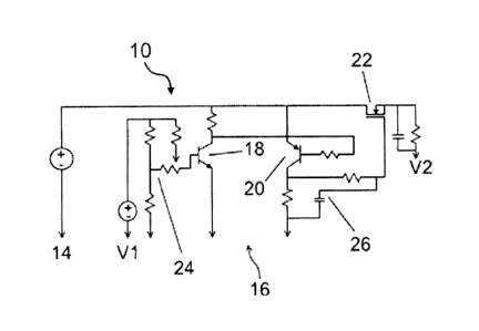
A power supply control apparatus according to a first embodiment of the
invention
is shown in Figure 1 and is designated generally by the reference numeral 10.
This
embodiment is described with reference to its use to control the supply of
power to
a FPGA device 12, but it will be appreciated that this embodiment can also be
used
to control the supply of power to other types of electronic devices.
In use, the power supply control apparatus 10 interconnects a power source 14
and a plurality of electrical inputs of the FPGA device 12 so that the power
supply
control apparatus 10 is operable to permit the supply of power from the power
source 14 to each electrical input. In the embodiment shown, each electrical
input
of the FPGA device is in the form of a voltage rail V1, V2, V3, Vn.
The power supply control apparatus 10 comprises a power supply sequencer
circuit and a power supply control element. The power supply sequencer circuit
includes a power supply sequencer stage 16, which includes first and second
circuit elements in the form of first and second IGBTs 18, 20. The power
supply
control element is in the form of a n-channel MOSFET 22 configured to function
as
a load switch.
A first V1 of the voltage rails of the FPGA device 12 is operatively connected
to the
gate of the first IGBT 18 via a voltage divider 24. The values of the
resistors of the
voltage divider 24 are configured so that a positive (or high) indication
signal is
provided as an input signal to the gate of the first IGBT 18 to turn it on
when a
voltage of the first voltage rail V1 reaches or passes a predefined voltage
threshold, and so that a negative (or low) indication signal is provided as an
input
signal to the gate of the first IGBT 18 to turn it off for all other values of
the voltage
of the first voltage rail V1.
6
1 CA 3032135 2019-01-31
319629-2
The power source 14 is connected, in use, to a drain of the n-channel MOSFET
22. A second V2 of the voltage rails of the FPGA device 12 is operatively
connected to a source of the n-channel MOSFET 22. This configuration of the n-
channel MOSFET 22 enables the connection of the power source 14 to the second
voltage rail V2 when the n-channel MOSFET 22 is turned on, and the
disconnection of the power source 14 from the second voltage rail V2 when the
n-
channel MOSFET 22 is turned off.
The collector of the first IGBT 18 is connected in shunt with the first
voltage rail V1,
and is also operatively connected to the gate of the second IGBT 20. This
configuration of the collector of the first IGBT 18 means that:
= when the first IGBT 18 is turned off, the voltage at the collector of the
first
IGBT 18 is sufficiently large to provide a positive intermediate signal to the
gate of the second IGBT 20 to turn it on; and
= when the first IGBT 18 is turned on, the voltage at the collector of the
first
IGBT 18 is sufficiently low to provide a negative intermediate signal to the
gate of the second IGBT 18 to turn it off.
The emitter of the second IGBT 20 is connected in shunt with the first voltage
rail
V1. The collector of the second IGBT 20 is operatively connected to the gate
of
the n-channel MOSFET 22 via a resistor-capacitor filter 26. This configuration
of
the second IGBT 20 means that:
= when the second IGBT 20 is turned off, the voltage at the collector of
the
second IGBT 20 is sufficiently large to provide a positive control signal to
the gate of the n-channel MOSFET 22 to turn it on; and
= when the second IGBT 20 is turned on, the voltage at the collector of the
second IGBT 20 is sufficiently large to provide a negative control signal to
the gate of the n-channel MOSFET 22 to turn it off.
7
CA 3032135 2019-01-31
319629-2
It is envisaged that, in other embodiments of the invention, each IGBT 18, 20
may
be replaced by another type of switching element, a logic element, or a
comparator
element. It is also envisaged that, in still other embodiments of the
invention, the
n-channel MOSFET 22 may be replaced by another type of switching element. It
will be appreciated that the resistor-capacitor filter 26 is an optional
feature of the
embodiment, and may be omitted or replaced by another type of electronic
filter.
A power sequencing procedure of the power supply control apparatus 10 of
Figure
1 is described as follows with reference to Figures 3 and 4.
Initially, before the first voltage rail V1 is connected to the power source
14, the
first voltage rail V1 is at a voltage level which has not reached or passed
the
predefined voltage threshold. At this stage the negative indication signal is
provided as the input signal to the gate of the first IGBT 18 to turn it off,
which
results in the provision of a positive intermediate signal to the gate of the
second
IGBT 20 and therefore the turn-on of the second IGBT 20. As a result, the
negative
control signal is provided to the gate of the n-channel MOSFET 22 to trigger
its
turn-off, thus disconnecting the power source 14 from the second voltage rail
V2.
When power is supplied from the power source 14 to the first voltage rail V1,
the
voltage 28 of the first voltage rail V1 climbs until it reaches the predefined
voltage
threshold, as shown in Figure 3. This results in the generation of the
positive
indication signal, which turns on the first IGBT 18 and thereby causes the
voltage
of the collector of the first IGBT 18 to drop to a value sufficiently low to
provide a
negative intermediate signal to the gate of the second IGBT 20. This in turn
triggers the turn-off of the second IGBT 20 to cause the voltage of the
collector of
the second IGBT 20 to rise to a level which provides a positive control signal
to the
gate of the n-channel MOSFET 22. This triggers the turn-on of the n-channel
MOSFET 22 so that the power source 14 is now connected to the second voltage
rail V2, thus permitting the supply of power to the second voltage rail V2.
This
8
CA 3032135 2019-01-31
319629-2
results in an increase in voltage 30 of the second voltage rail V2, as shown
in
Figure 3.
The above power sequencing procedure is described with reference to supply of
power to the first and second voltage rails V1, V2, but it will be appreciated
that
the above power sequencing procedure is applicable to any two of the voltage
rails
V1, V2, V3, Vn of the FPGA device 12.
The arrangement of the first and second IGBTs 18,20 in the power sequencer
stage 16 provides a delay, typically in the range of milliseconds, between the
voltage 28 of the first voltage rail V1 reaching or passing the predefined
voltage
threshold and the turn-on of the n-channel MOSFET 22, thus providing a delay
between the supply of power between the first and second voltage rails V1, V2.
Furthermore, the values of the resistor and capacitor in the resistor-
capacitor filter
26 may be configured to further modify the amount of delay, typically in the
range
of milliseconds, between the supply of power between the first and second
voltage
rails V1, V2. Such a delay not only is independent of the voltage ramp rate of
the
power supplied by the power source 14, but also can be configured to introduce
a
"soft-start" 32 to the supply of power to the second voltage rail V2 to avoid
the
problem of inrush current, as shown in Figure 4.
The reliability and efficiency of the power sequencing procedure is therefore
enhanced by the configuration of the power supply sequencer circuit in the
power
supply control apparatus 10 of Figure 1 which permits the provision of a
stable and
customisable delay between the supply of power to the voltage rails V1, V2,
V3,
Vn of the FPGA device 12.
The signal generation sequence of the power supply sequencer stage 16 permits
a simpler and more cost-effective design of the power supply sequencer circuit
by
allowing the use of the IGBTs 18,20, and removes the requirements for costlier
power good pins. Also, the removal of the need for power good pins permits the
9
CA 3032135 2019-01-31
319629-2
use of the invention with low cost voltage regulators without power good pins,
such
as dc-dc converters and low-dropout regulators.
In addition, the above-described signal generation sequence of the power
supply
sequencer stage 16 results in a safer power sequencing procedure. If the power
supply sequencer circuit is instead designed to provide a negative control
signal to
trigger the n-channel MOSFET 22, the power supply sequencer circuit will
continue
to provide the negative control signal even when the power supply control
apparatus 10 is not working properly, thus resulting in accidental triggering
of the
n-channel MOSFET 22. On the other hand, designing the power supply sequencer
circuit to provide a positive control signal to trigger the n-channel MOSFET
22
means that the power supply sequencer circuit would not accidentally trigger
the
n-channel MOSFET 22 due to the output of the power supply sequencer circuit
reverting to a negative signal when the power supply control apparatus 10 is
not
working properly.
Moreover, using the n-channel MOSFET 22 as the load switch is more reliable,
cheaper and consume less power than using a p-channel MOSFET 22 as the load
switch.
A power supply control apparatus according to a second embodiment of the
invention is shown in Figure 5 and is designated generally by the reference
numeral 110. The power supply control apparatus 110 of Figure 5 is similar in
structure and operation to the power supply control apparatus 10 of Figure 1
and
like features share the same reference numerals.
The power supply control apparatus 110 of Figure 5 differs from the power
supply
control apparatus 10 of Figure 1 in that, in the power supply control
apparatus 110
of Figure 5, the power supply sequencer circuit includes first and second
power
supply sequencer stages 116, 216, instead of the single power supply sequencer
stage 16 shown in Figure 1.
CA 3032135 2019-01-31
319629-2
The first power supply sequencer stage 116 in Figure 5 is similar in structure
to the
power supply sequencer stage in Figure 1, and the second power supply
sequencer stage 216 is arranged between the first power supply sequencer stage
116 and the gate of the n-channel MOSFET 22. The second power supply
sequencer stage 216 includes first and second IGBTs 118, 120, with a collector
of
the first IGBT 118 connected to the gate of the second IGBT1 20 and with the
collector of the second IGBT 120 connected to the gate of the n-channel MOSFET
22. The collector of the second IGBT 20 of the first power supply sequencer
stage
116 is connected to a gate of the first IGBT 118 of the second power supply
sequencer stage 216. A DC voltage source 34 is connected to the collector of
the
first IGBT 118 of the second power supply sequencer stage 216, and is
connected
across the second IGBT 120 of the second power supply sequencer stage 216.
The configuration of the second power supply sequencer stage 216 means that:
= when the second IGBT 20 of the first power supply sequencer stage 116 is
turned off, the voltage at the collector of the second IGBT 20 of the first
power supply sequencer stage 116 is sufficiently large to provide a positive
input signal to the gate of the first IGBT 118 of the second power supply
sequencer stage 216 to turn it on;
= when the second IGBT 20 of the first power supply sequencer stage 116 is
turned on, the voltage at the collector of the second IGBT 20 of the first
power supply sequencer stage 116 is sufficiently low to provide a negative
input signal to the gate of the first IGBT 118 of the second power supply
sequencer stage 216 to turn it off;
= when the first IGBT 118 of the second power supply sequencer stage 216
is turned off, the voltage at the collector of the first IGBT 118 of the
second
power supply sequencer stage 216 is sufficiently large to provide a positive
intermediate signal to the gate of the second IGBT 120 of the second power
supply sequencer stage 216 to turn it on;
11
CA 3032135 2019-01-31
319629-2
= when the first IGBT 118 of the second power supply sequencer stage 216
is turned on, the voltage at the collector of the first IGBT 118 of the second
power supply sequencer stage 216 is sufficiently low to provide a negative
intermediate signal to the gate of the second IGBT 120 to turn it off;
= when the second IGBT 120 of the second power supply sequencer stage
216 is turned off, the voltage at the collector of the second IGBT 120 of the
second power supply sequencer stage 216 is sufficiently large to provide a
positive control signal to the gate of the n-channel MOSFET 22 to turn it on;
and
= when the second IGBT 120 of the second power supply sequencer stage
216 is turned on, the voltage at the collector of the second IGBT 120 of the
second power supply sequencer stage 216 is sufficiently large to provide a
negative control signal to the gate of the n-channel MOSFET 22 to turn it
off.
A power sequencing procedure for the power supply control apparatus 110 of
Figure 5 is described as follows.
Initially, before the first voltage rail V1 is connected to the power source
14, the
first voltage rail V1 is at a voltage level which has not reached or passed
the
predefined voltage threshold. At this stage the negative indication signal is
provided as the input signal to the gate of the first IGBT 18 of the first
power supply
sequencer stage 116 to turn it off, which results in the provision of a
positive
intermediate signal to the gate of the second IGBT 20 of the first power
supply
sequencer stage 116 and therefore the turn-on of the second IGBT 20 of the
first
power supply sequencer stage 116. In turn, this triggers the turn-off of the
first
IGBT 18 and the turn-on of the second IGBT 20 of the second power supply
sequencer stage 216. As a result, the negative control signal is provided to
the
gate of the n-channel MOSFET 22 to trigger its turn-off, thus disconnecting
the
power source 14 from the second voltage rail V2.
12
CA 3032135 2019-01-31
1
319629-2
When power is supplied from the power source 14 to the first voltage rail V1,
the
voltage of the first voltage rail V1 climbs until it reaches the predefined
voltage
threshold. This results in the generation of the positive indication signal,
which
turns on the first IGBT 18 of the first power supply sequencer stage 116 and
thereby causes the voltage of the collector of the first IGBT 18 of the first
power
supply sequencer stage 116 to drop to a value sufficiently low to provide a
negative
intermediate signal to the gate of the second IGBT 20 of the first power
supply
sequencer stage 116. This in turn triggers the turn-off of the second IGBT 20
of
the first power supply sequencer stage 116 to cause the voltage of the
collector of
the second IGBT 20 of the first power supply sequencer stage 116 to rise to a
level
which provides a positive input signal to turn on the first IGBT 118 of the
second
power supply sequencer stage 216. This subsequently leads to the provision of
a
negative intermediate signal to the second IGBT 120 of the second power supply
sequencer stage 216 to turn it off, thus providing a positive control signal
to the
gate of the n-channel MOSFET 22. This triggers the turn-on of the n-channel
MOSFET 22 so that the power source 14 is now connected to the second voltage
rail V2, thus permitting the supply of power to the second voltage rail V2.
This
results in an increase in voltage of the second voltage rail V2.
The addition of the second power supply sequencer stage 216 adds a further
delay
to the overall delay between the supply of power to different voltage rails
V1, V2 of
the FPGA device 12. The cascade arrangement of the first and second power
supply sequencer stages 116, 216 therefore allows for further customisation of
the
delay between the supply of power to different voltage rails V1, V2 of the
FPGA
device 12. More particularly, the amount of delay can be increased by further
increasing the number of power supply sequencer stages in the cascade
arrangement.
13
I CA 3032135 2019-01-31