Note: Descriptions are shown in the official language in which they were submitted.
CA 03032224 2019-01-28
WO 2018/018161 PCT/CA2017/050914
METHODS OF ELECTROCHEMICAL DEPOSITION
Reference to Related Applications
[0001] This application claims priority from U.S. Patent Application Ser. No.
62/368292,
entitled METHOD OF ELECTROCHEMICAL DEPOSITION, filed July 29, 2016 which is
hereby incorporated herein by this reference in its entirety for all purposes.
For purposes of
the United States of America this application claims the benefit of U.S.
Patent Application
Ser. No. 62/368292, entitled METHOD OF ELECTROCHEMICAL DEPOSITION, filed July
29, 2016.
Technical Field
[0002] This application relates to textured layers of metallic materials,
textured
nanocrystals, core-shell nanoparticles having a textured shell., and methods
of
electrochemical deposition for producing textured layers of metallic
materials, textured
nanocrystals, and core-shell nanoparticles having a textured shell.
Background
[0003] The controlled formation of nanostructures and the deposition of
metals, metal
alloys, and metal-containing compounds represents an important aspect of many
modern
day technologies, including, without limitation, semiconductor fabrication
(e.g. forming metal
interconnects), use of planar and nanostructured metal films in plasmonic,
nanophotonic,
and meta-material applications, deposition of patterned, high aspect ratio
metal structures
for X-ray optics, production of energy conversion technologies and sensors,
use of metals,
metal alloys, and metal nanostructures for catalyzing chemical reactions, use
of magnetic
alloy materials for magnetic storage applications, etc. For these and related
technologies,
such as those requiring metal nanowires, there may be a desire for patterning
of metallic
materials at smaller size scales than those that are currently employed.
Improved methods
for their controlled formation will may also be desirable.
[0004] Metal nanoparticles play important roles in many different
technological and
commercial applications. For example, metal nanoparticles serve as a model
system to
experimentally probe the effects of quantum-confinement on electronic,
magnetic, and other
related properties. They have also been widely exploited for use in
photography, catalysis,
biological labeling, photonics, optoelectronics, information storage, surface-
enhanced
1
CA 03032224 2019-01-28
WO 2018/018161 PCT/CA2017/050914
Raman scattering (SERS), and formulation of magnetic ferrofluids. The
intrinsic properties
of metal nanoparticles may be related to a number of parameters which include,
without
limitation, their size, shape, composition, crystallinity, and structure.
These parameters can
be used to control the properties of the nanoparticles. For example, the
plasmon resonance
features of gold or silver nanorods have been shown to have a strong
dependence on the
aspect-ratios of these nanostructures. The sensitivity of SERS has also been
demonstrated
to depend on the morphology of a silver nanoparticle. Silver nanoparticles are
also subject
to oxidation, which limits their stability and utility in many different
environments. One
strategy that has been proposed to circumvent this shortcoming is to
encapsulate the silver
nanoparticle with a thin layer of gold, since gold is significantly more
resistant to oxidation
than silver. However, attempts to reduce gold onto silver nanoparticles are
limited by so-
called galvanic replacement, where gold ion (Au3 ) reduction comes at the
expense of silver
(Ag) oxidation, resulting in porous, mixed composition structures with
undesirable SERS
response. United States patent No. 9,394,168 entitled "Methods of
nanostructure formation
.. and shape selection" describes methods to take advantage of porous
nanostructures
formed in this manner, due to their relatively lower density and higher
surface area than
their solid counterparts. However, the ability to make Au/Ag core-shell
nanoparticles
without compromising the integrity of the silver core would extend the SERS
activity and
stability of these structures, as well as offer new plasmonic applications.
Thus, there
.. remains a desire to develop new methods of metal reduction that mitigate
the effects of
galvanic replacement.
[0005] The electrochemical deposition of metals, metal alloys, and metal-
containing
compounds is widely used in many industries and represents a versatile and
inexpensive
deposition method. However, in many cases, the quality of electrochemical
deposition is
subject to kinetic and thermodynamic factors that limit the fidelity and
crystallinity of the
resulting deposited material. For example, the rates of nucleation and growth
in
conventional electrodeposition and electroless deposition of metallic
materials often result in
polycrystalline deposition characterized by voids, defects, and grain
boundaries that can
limit performance in certain applications. Due to losses at grain boundaries
and defects,
such materials typically have poor performance characteristics and compromised
thermal
and mechanical stabilities. For example, the resistivity of a material
increases as a result of
imperfections, such as defects, impurities, grain boundaries, and dislocations
(see Ziman,
2
CA 03032224 2019-01-28
WO 2018/018161 PCT/CA2017/050914
J.M. "Electrons and Phonons", Clarendon Press, Oxford, 1960). Conventional
attempts to
improve the quality of the materials resulting from electrochemical deposition
rely on the
use of additives and stabilizers in the electrochemical bath. United States
patent No.
4,525,390 entitled "Deposition of Copper From Electroless Plating
Compositions" describes
electrochemical bath compositions and methods to reduce the number of voids
and nodules
encountered during copper deposition into printed circuit board interconnects.
These voids
may lead to unreliable electrical connections and cracking in printed circuit
boards, while
nodules may result in unwanted short circuits between printed circuit board
elements.
[0006] The ability to form nanocrystals and core-shell nanoparticles and to
deposit
crystalline metallic materials using electrochemical reduction methods is
anticipated to
provide opportunities for improved performance of existing technologies as
well as the
development of new technologies. There are some known methods for depositing
crystalline metallic materials. However, most of these known methods use high
vacuum or
ultrahigh vacuum methods (such as molecular beam epitaxy, vapor phase epitaxy,
and
.. atomic layer epitaxy) or high temperature furnaces (such as in liquid phase
epitaxy). As a
result, these methods are costly and time consuming. United States patent No.
6,670,308
entitled "Method of Depositing Epitaxial Layers on a Substrate" describes
electrochemical
deposition methods to produce substantially single orientation epitaxial
layers. Sodium
borohydride and sodium hypophosphate are used as reducing agents for
electrochemical
deposition. Such reducing agents oxidize substrates susceptible to galvanic
replacement in
the presence of a metal salt (e.g. silver (Ag)).
[0007] Improved control over metallic material deposition remains a
significant challenge
for many technologies and new methods that achieve crystalline material
deposition
electrochemically are extremely desirable. Therefore, there is a desire for
improved
.. methods for forming textured nanocrystals and core-shell nanoparticles
having a textured
shell, and for the electrochemical deposition of textured layers of metallic
materials on
substrates including, but not limited to, single-crystal substrates, patterned
substrates, and
articles formed on a substrate.
[0008] The foregoing examples of the related art and limitations related
thereto are intended
to be illustrative and not exclusive. Other limitations of the related art
will become apparent
to those of skill in the art upon a reading of the specification and a study
of the drawings.
3
CA 03032224 2019-01-28
WO 2018/018161 PCT/CA2017/050914
Summary
[0009] The following embodiments and aspects thereof are described and
illustrated in
conjunction with systems, tools and methods which are meant to be exemplary
and
illustrative, not limiting in scope. In various embodiments, one or more of
the above-
described problems have been reduced or eliminated, while other embodiments
are
directed to other improvements.
[0010] One aspect of the invention provides a method of electrochemical
deposition of a
metallic material onto a substrate. The method includes providing an alkaline
solution of
hydroxide ions, immersing a metallic material precursor and the substrate into
the alkaline
.. solution to form an electrochemical bath, and electrochemically depositing
a textured layer
of the metallic material onto the substrate.
[0011] Another aspect of the invention provides a method electrochemical
deposition of a
textured nanoparticle. The method includes providing an alkaline solution of
hydroxide ions,
immersing the metallic material into the alkaline solution to form an
electrochemical bath,
and precipitating the textured nanoparticles from the electrochemical bath.
[0012] Another aspect of the invention provides a method of electrochemical
deposition of a
metallic material onto a nanoparticle. The method includes providing an
alkaline solution of
hydroxide ions, immersing the metallic material and the nanoparticle into the
alkaline
solution to form an electrochemical bath, and depositing a textured layer of
the metallic
material onto the nanoparticle.
[0013] Further aspects of the invention are described in the claims.
[0014] In addition to the exemplary aspects and embodiments described above,
further
aspects and embodiments will become apparent by reference to the drawings and
by study
of the following detailed descriptions.
Brief Description of the Drawings
[0015] Exemplary embodiments are illustrated in referenced figures of the
drawings. It is
intended that the embodiments and figures disclosed herein are to be
considered illustrative
rather than restrictive.
4
CA 03032224 2019-01-28
WO 2018/018161 PCT/CA2017/050914
[0016] Figure 1 is a flow chart which illustrates methods for electrochemical
deposition of a
textured layer of a metallic material on a substrate according to an example
embodiment of
the present invention.
[0017] Figure 2A is a schematic illustration of an epitaxial layer of a
metallic material
deposited on a single-crystal substrate according to an example embodiment of
the present
invention.
[0018] Figure 2B is a schematic illustration of a single-crystal substrate
coated with two
epitaxial layers of metallic materials according to an example embodiment of
the present
invention.
[0019] Figure 2C is a schematic illustration of a single-crystal substrate
upon which is
deposited a metal alloy according to an example embodiment of the present
invention.
[0020] Figure 3A is a schematic illustration of a substantially crystalline
substrate upon
which is deposited a locally resonant surface plasmons (LRSP) active element
according to
an example embodiment of the present invention.
[0021] Figure 3B is a schematic illustration of a substantially crystalline
substrate upon
which is deposited LRSP-mediated reduction on LRSP active elements according
to an
example embodiment of the present invention.
[0022] Figure 4A is a schematic illustration of a variety of shaped
crystallites supported by a
substantially crystalline substrate according to an example embodiment of the
present
invention.
[0023] Figure 4B is a schematic illustration of an epitaxial layer of a
metallic material
deposited on the variety of shaped crystallites and substrate of FIG. 4A
substrate according
to an example embodiment of the present invention.
[0024] Figure 5A is a schematic illustration of a epitaxial deposition of
metallic material in
the presence of one or more shape-control agents (i.e. shape-controlled
epitaxy)
demonstrating homoepitaxial deposition of square pyramidal crystallites onto a
patterned
substrate (i.e. additive deposition) according to an example embodiment of the
present
invention.
5
CA 03032224 2019-01-28
WO 2018/018161
PCT/CA2017/050914
[0025] Figure 5B is a schematic illustration of a shape-controlled epitaxy
demonstrating
heteroepitaxial deposition of cuboid crystallites onto a patterned substrate
according to an
example embodiment of the present invention.
[0026] Figure 6A is a flow chart which illustrates methods for forming
textured nanoparticles
and core-shell nanoparticles having a textured shell according to example
embodiments of
the present invention.
[0027] Figure 6B is a flow chart which illustrates methods for forming core-
shell
nanoparticles having a textured shell according to an example embodiment of
the present
invention.
[0028] Figure 7 is a two-dimensional X-ray diffraction (2D-XRD) pattern of a
polycrystalline
gold layer deposited on a single-crystal Ag(100) substrate under conditions
that lead to
surface oxidation by galvanic replacement.
[0029] Figure 8 is a 2D-XRD pattern of an epitaxial, single-crystal gold layer
deposited on a
single-crystal Ag(100) substrate according to the methods described in Example
1.
[0030] Figure 9 is a cross-sectional scanning electron microscopy (SEM) image
of an
epitaxial, single-crystal gold layer deposited on a single-crystal Ag(100)
substrate prepared
according to the methods described in Example 1.
[0031] Figure 10A is a high resolution cross-sectional transmission electron
microscopy
(TEM) image (scale bar 200 nm) of an epitaxial, single-crystal gold layer
deposited on a
single-crystal Ag(100) substrate according to the methods described in Example
1.
[0032] Figure 10B is a high resolution cross-sectional TEM image (scale bar 20
nm) of the
plated substrate highlighted region shown in Figure 10A, with higher
resolution.
[0033] Figure 10C is an expanded high resolution cross-sectional TEM image of
the plated
substrate highlighted region shown in Figure 10B, demonstrating the alignment
and
registration of metal atoms across the interface.
[0034] Figure 10D is a cross-sectional selected area electron diffraction
pattern of the
highlighted region of the plated substrate shown in Figure 10C.
[0035] Figure 11A is a top view SEM image (scale bar 500 nm)of an epitaxial,
single-crystal
gold layer deposited on a single-crystal Ag(100) substrate according to the
methods
described in Example 1.
6
CA 03032224 2019-01-28
WO 2018/018161 PCT/CA2017/050914
[0036] Figure 11B is an atomic force microscopy (AFM) image (2 x 2 pm2) of the
plated
substrate shown in Figure 11A.
[0037] Figure 11C is a top view SEM image (scale bar 500 nm)of a physical
vapor
deposition (PVD) deposited gold film on a single-crystal Si(100) substrate
containing a5 nm
thick Cr adhesion layer..
[0038] Figure 11D is an AFM image (2 x 2 1im2) of the plated substrate shown
in Figure
11C.
[0039] Figure 12A is a schematic illustration of a substantially crystalline
substrate coated
with a sacrificial resist containing pores according to an example embodiment
of the present
invention.
[0040] Figure 12B is a schematic illustration of patterned epitaxial surface
features
deposited in the pores of the patterned substrate depicted in Figure 13A,
following removal
of the sacrificial resist, according to an example embodiment of the present
invention.
[0041] Figure 12C is a schematic illustration of a substantially crystalline
substrate
containing pores and a sacrificial layer according to an example embodiment of
the present
invention.
[0042] Figure 12D is a schematic illustration of patterned epitaxial surface
features
deposited into the pores on the substrate shown in FIG. 13C following removal
of the
sacrificial layer.
[0043] Figure 13A is a top view SEM image (2 pm scale bar) of two rings
patterned by FIB-
milled in a PVD-deposited polycrystalline gold layer deposited on a single-
crystal Si(100)
substrate (left) and the same two features FIB-patterned in an epitaxial gold
layer deposited
on a single-crystal Ag(100) substrate (right) according to the methods
described in Example
1.
[0044] Figure 13B is a top view SEM image (500 nm scale bar) of a series of
holes FIB-
milled in the PVD-deposited polycrystalline gold layer (left) and in an
epitaxial Au(100) layer
(right) according to the methods described in Example 1.
[0045] Figure 13C is a top view SEM image (2 pm scale bar) of a series of
lines FIB-milled
in the PVD-deposited polycrystalline gold layer (left) and in an epitaxial
Au(100) layer (right)
according to the methods described in Example 1.
7
CA 03032224 2019-01-28
WO 2018/018161
PCT/CA2017/050914
[0046] Figure 13D is a top view SEM image (2 pm scale bar) of a series of FIB-
milled
windows in the PVD-deposited polycrystalline gold layer (left) and in an
epitaxial Au(100)
layer (right) according to the methods described in Example 1.
[0047] Figure 13E is a top view SEM image (1 pm scale bar) of a bow-tie
antenna FIB-
milled in the PVD-deposited polycrystalline gold layer (left) and in an
epitaxial Au(100) layer
(right) according to the methods described in Example 1.
[0048] Figure 14A is a schematic illustration of patterned pillars deposited
on a substantially
crystalline substrate according to an example embodiment of the present
invention.
[0049] Figure 14B is a schematic illustration of the FIG. 15A patterned
pillars coated with an
epitaxial layer of a metallic material according to an example embodiment of
the present
invention.
[0050] Figure 15A shows a top view SEM image (5 pm scale bar) of a gold-coated
silver
nanopillar array with 550 nm pillar periodicity according to the methods
described in
Example 3.
[0051] Figure 15B shows a confocal microscope image (2 pm scale bar) of two-
photon
photoluminescence (2PPL) emanating from the gold-coated silver pillar array
shown in FIG.
16A, following excitation with a pulsed laser centered at 735 nm wavelength.
[0052] Figure 15C shows an enlarged image of the confocal microscope image of
2PPL
shown in FIG. 15B.
[0053] Figure 16A is a top view SEM image (5 pm scale bar) of an epitaxial,
crystalline
silver nanopillar array formed on a Ag(100) single-crystal substrate using
electron beam
lithography patterning, as illustrated in FIGS. 11A and 11B, according to the
methods
described in Example 3.
[0054] Figure 16B is a tilt view SEM image (300 nm scale bar) of an individual
pillar shown
.. in FIG. 16A. The pillar demonstrates faceting expected from a feature
deposited epitaxially
on the Ag(100) substrate.
[0055] Figure 16C is a top view SEM image (200 nm scale bar) of an individual
pillar shown
in FIG. 16A. The top view image shows the presence of crystal facets.
[0056] Figure 16D is a top view SEM image of the pillar shown in FIG. 16C
coated with a
.. thin -10 nm layer of gold according to an example embodiment of the present
invention.
8
CA 03032224 2019-01-28
WO 2018/018161 PCT/CA2017/050914
The coated pillar retains its facted characteristics, implying that the
deposited gold overlayer
is heteroepitaxial.
[0057] Figure 17 shows a top view SEM image (300 pm scale bar) of a portion of
a
rectangle-based nanowire structure patterned by electron beam lithography
(EBL). High
.. aspect ratio crystalline gold nanowires displaying narrow widths over long
distances) have
been deposited on a single crystal Ag(100) substrate according to an example
embodiment
of the present invention. Inset (left) (300 nm scale bar) demonstrates
nanowire widths of
about 40 nm Inset (lower) (500 nm scale bar) demonstrates continuous
crystalline wire
characteristics.
[0058] Figure 18 shows a top view SEM image (500 nm scale bar) of nanometer-
scale gold
square pyramids deposited on a single crystal Ag(100) substrate according to
an example
embodiment of the present invention. Gold deposition in the presence of the
shape control
agent Na2SO4 yields a textured gold film characterized by oriented square
pyramids
registered with the underlying substrate. Inset (right) shows an expanded view
of the
highlighted area showing smoothly-faceted oriented square pyramids.
[0059] Figure 19 shows a top view SEM image (5 pm scale bar) of gold square
pyramids
containing corkscrew defects deposited on a single crystal Ag(100) substrate
according to
an example embodiment of the present invention. Gold deposition in the
presence of the
shape control agent NaCI yields a textured gold film characterized by oriented
square
pyramids comprising corkscrew defects registered with the underlying
substrate. Inset (let)
shows an expanded view of a single pyramid highlighting the non-uniform facet
morphology
of the oriented square pyramids.
[0060] Figure 20 shows a top view SEM image (200 nm scale bar) of nanometer-
scale
copper square pyramids deposited in the presence of the shape control agent
Na2SO4 on a
.. single crystal Au(100) substrate patterned by electron beam lithography
according to an
example embodiment of the present invention. Deposition is seen to occur only
in the pores
and yields smoothly faceted square pyramids with orientations registered with
the
underlying substrate.
[0061] Figure 21 shows a top view SEM image (2 pm scale bar) of nanometer-
scale gold
square pyramids deposited on a single crystal Ag(100) substrate according to
an example
embodiment of the present invention. Gold deposition in the presence of the
shape control
9
CA 03032224 2019-01-28
WO 2018/018161
PCT/CA2017/050914
agent S042- from the metal material precursor yields a textured gold film
characterized by
smoothly faceted oriented square pyramids registered with the underlying
substrate.
[0062] Figure 22A shows a high-angle annular dark-field (HAADF) transmission
electron
microscopy image (90 nm scale bar) of a silicon-supported single crystal
silver Ag(100)
.. substrate deposited sequentially with gold (Au) and platinum (Pt) to yield
a film containing a
mixture of metals according to an example embodiment of the present invention.
[0063] Figure 22B shows an expanded TEM image (70 nm scale bar) of the region
highlighted in Figure 22A with elemental mapping contrast. The image
highlights the
location of silicon in the multilayer structure.
[0064] Figure 22C shows an expanded TEM image (70 nm scale bar) of the region
highlighted in Figure 22A with elemental mapping contrast. The image
highlights the
location of silver in the multilayer structure.
[0065] Figure 22D shows an expanded TEM image (70 nm scale bar) of the region
highlighted in Figure 22A with elemental mapping contrast. The image
highlights the
.. location of gold in the multilayer structure.
[0066] Figure 22E shows an expanded TEM image (70 nm scale bar) of the region
highlighted in Figure 22A with elemental mapping contrast. The image
highlights the
location of platinum in the multilayer structure.
[0067] Figure 23 shows a two-dimensional X-ray diffraction (2D-XRD) pattern of
single-
crystal Pt(100) deposited on single-crystal Ag(100) as evidenced by the highly
localized
Pt(200) diffraction intensity distribution.
[0068] Figure 24A shows a one-dimensional X-ray diffraction (1D-XRD) pattern
of single-
crystal Pt(100) on single crystal Ag(100) according to an example embodiment
of the
present invention.
.. [0069] Figure 24B shows a one-dimensional X-ray diffraction (1D-XRD)
pattern of a single-
crystal PtAu(100) alloy formed from a 1:1 molar ratio of Pt- and Au-containing
metal salts in
the electrochemical bath deposited on single crystal Ag(100) according to an
example
embodiment of the present invention.
[0070] Figure 24C shows a one-dimensional X-ray diffraction (1D-XRD) pattern
of a single-
crystal PtAg(100) alloy formed from a 1:1 molar ratio of Pt- and Ag-containing
metal salts in
CA 03032224 2019-01-28
WO 2018/018161 PCT/CA2017/050914
the electrochemical bath deposited on single crystal Ag(100) according to an
example
embodiment of the present invention.
[0071] Figure 25 shows an X-ray photoelectron spectroscopy (XPS) graph showing
the
XPS energies of Pt and PtAu (1:1) and PtAg (1:1) alloys deposited according to
an example
embodiment of the present invention.
[0072] Figure 26A shows a graph of linear sweep voltammograms performed in 1.0
M
NaOH to assess the catalytic activities of a series of PtxAgyalloy catalysts
according to an
example embodiment of the present invention.
[0073] Figure 26B shows a graph of linear sweep voltammograms performed in 1.0
M
NaOH to assess the catalytic activities of a series of PtxAuy alloy catalysts
according to an
example embodiment of the present invention.
[0074] Figure 27A shows a top view SEM image (500 nm scale bar) of a single
crystal
platinum Pt(100) film deposited on single crystal Ag(100) according to an
example
embodiment of the present invention. The morphology of the resulting film is
substantially
flat and smooth.
[0075] Figure 27B shows a top view SEM image (1 pm scale bar) of a platinum Pt
film
deposited on single crystal Au(100) according to an example embodiment of the
present
invention. The morphology of the resulting film is significantly different
from that obtained
by deposition on single crystal Ag(100), demonstrating the substrate dependent
nature of
the deposition.
Description
[0076] Throughout the following description specific details are set forth in
order to provide
a more thorough understanding to persons skilled in the art. However, well
known elements
may not have been shown or described in detail to avoid unnecessarily
obscuring the
disclosure. Accordingly, the description and drawings are to be regarded in an
illustrative,
rather than a restrictive, sense.
[0077] Unless context dictates otherwise, "metallic material" (as used herein)
refers to a
metal, a metal alloy, a metal containing compound, a metallic material
precursor, and
mixtures thereof.
11
CA 03032224 2019-01-28
WO 2018/018161 PCT/CA2017/050914
[0078] Unless context dictates otherwise, "metallic material precursor" (as
used herein)
refers to a solid anode comprising a metal, a metal alloy, a metal containing
compound, and
mixtures thereof and/or a salt of a metal, a metal alloy, a metal containing
compound, or
mixtures thereof.
[0079] Unless context dictates otherwise, "metal alloy" (as used herein)
refers to a
homogenous mixture of two or more metals.
[0080] Unless context dictates otherwise, "non-metal" (as used herein) refers
to elements of
the periodic table that are not a metal, chemical species that do not contain
a metal, and
mixtures thereof.
[0081] Unless context dictates otherwise, "metal-containing compound" (as used
herein)
refers to a compound that contains one or more metals. A metal-containing
compound
includes, but is not limited to, a coordination complex comprising a central
metal atom or
metal ion (i.e. the coordination centre) and a surrounding array of bound
molecules or ions
(i.e. the ligands or chemical species that contains one or more metallic
elements. Examples
include, but are not limited to, aluminum oxide (A1203), copper oxide (Cu2O),
zinc oxide
(Zn0), cobalt monoxide (Co0), etc.
[0082] Unless context dictates otherwise, "uniform alloy composition" (as used
herein)
refers to the alloy composition of a deposition layer, wherein the
distribution of the different
metals is consistent throughout the thickness of the layer.
[0083] Unless context dictates otherwise, "substrate" (as used herein) refers
to a catalytic or
non-catalytic solid material capable of supporting a layer of metallic
material deposited via
electrochemical deposition. The solid material is non-soluble under basic
conditions.
[0084] Unless context dictates otherwise, "polymeric material" (as used
herein) refers to a
large molecule, or macromolecule, formed by the polymerization of many smaller
molecules, called monomers, in a form that often, but not always, comprises a
repeating
structure.
[0085] Unless context dictates otherwise "substantially crystalline substrate"
(as used
herein) refers to a material that is formed by one or more of physical vapor
deposition,
chemical vapor deposition, molecular beam epitaxy, atomic layer deposition,
electrodeposition, electroless deposition, precipitation, diffusion, chemical
reaction, and
12
CA 03032224 2019-01-28
WO 2018/018161 PCT/CA2017/050914
combinations thereof. Substantially crystalline substrates also include
materials which have
grown in crystalline form from a melted material or using other conventional
methods that
can nucleate material for producing crystalline materials.
[0086] Unless context dictates otherwise, "epitaxial" (as used herein) refers
to an orientation
of a layer of a material deposited on the surface of a substrate, wherein the
layer mimics or
is registered with respect to the orientation of the surface of the underlying
substrate. The
two-dimensional X-ray diffraction (2D-XRD) pattern of an epitaxial layer
deposited on a
substrate via electrochemical deposition aligns with the 2D-XRD patterns of
the underlying
substrate. At least some of the atomic planes of the epitaxial layer and the
underlying
.. substrate, which may be observed via transmission electron microscopy, are
aligned.
[0087] Unless context dictates otherwise, "heteroepitaxy" and
"heteroepitaxial" (as used
herein) refer to the electrochemical deposition of a crystalline epitaxial
layer on a substrate
of a different kind of material.
[0088] Unless context dictates otherwise, "homoepitaxy" and "homoepitaxial"
(as used
herein) refer to the electrochemical deposition of a crystalline epitaxial
layer on a substrate
of the same kind of material.
[0089] Unless context dictates otherwise, "single-crystal" (as used herein)
refers to a
crystalline material in which the crystal lattice of the material is
continuous and unbroken to
the edges of the material, with no grain boundaries.
[0090] Unless context dictates otherwise, "crystalline" (as used herein)
refers to a chemical
material having a regular and periodic arrangement of atoms.
[0091] Unless context dictates otherwise, "polycrystalline" (as used herein)
refers to an
orientation of a layer of a material deposited on the surface of a substrate,
wherein the layer
comprises many crystallites of varying size and orientation with respect to
the orientation of
the surface of the underlying substrate. The two-dimensional X-ray diffraction
(2D-XRD)
pattern of a polycrystalline layer deposited on a substrate via
electrochemical deposition
does not align with the 2D-XRD patterns of the underlying substrate. The
atomic planes of
the polycrystalline layer and the underlying substrate, which may be observed
via
transmission electron microscopy, are not aligned.
13
CA 03032224 2019-01-28
WO 2018/018161 PCT/CA2017/050914
[0092] Unless context dictates otherwise, "textured" (as used herein) refers
to the
distribution of crystallographic orientations between fully polycrystalline
(e.g. powder) and
single-crystal.
[0093] Unless context dictates otherwise, "amorphous" (as used herein) refers
to a non-
crystalline material that is not textured.
[0094] Unless context dictates otherwise, "X-ray diffraction pattern" (as used
herein) refers
to the angle(s) at which X-rays are scattered by the atoms of a crystal.
[0095] Unless context dictates otherwise, "crystal" (as used herein) refers to
a material in
which the atoms are arranged in a rigid geometrical structure marked by
symmetry.
[0096] Unless context dictates otherwise, "electrochemical deposition" (as
used herein)
refers to electrodeposition, electroless deposition, and photoelectrochemical
deposition.
[0097] Unless context dictates otherwise, "electrodeposition" (as used herein)
refers to a
process that uses an externally supplied electric potential or electric
current to deposit a
layer of a metallic material on a substrate. The cathode substrate, a metallic
material
precursor, and an anode are immersed in an electrochemical bath. In some
embodiments,
electric potential or electric current is supplied to an anode comprising a
metallic material to
oxidize the metallic material and thereby produce a dissolved metallic
material precursor. In
some embodiments, the electrochemical bath comprising an oxidized form of the
metallic
material precursor dissolved in a liquid is supplied independently (e.g. in
the form of a
dissolved metal salt). The oxidized metallic material precursor is then
reduced at the
interface between the electrochemical bath and the cathode substrate and the
metallic
material is thereby deposited onto the surface of the substrate.
[0098] Unless context dictates otherwise, "electroless deposition" (as used
herein) refers to
a non-galvanic plating method in which a metallic material precursor and a
substrate are
contained in an electrochemical bath and used to deposit a layer of a metallic
material on a
substrate without the use of external electric potential or electric current.
[0099] Unless context dictates otherwise, "photoelectrochemical deposition"
(as used
herein) refers to a process to deposit a layer of a metallic material on a
substrate via
electrodeposition or electroless deposition in the presence of electromagnetic
radiation. In
14
CA 03032224 2019-01-28
WO 2018/018161 PCT/CA2017/050914
some embodiments, incident radiation induces redox reactions or produces
chemical
species that are capable of participating in redox reactions to thereby induce
deposition.
[0100] Unless context dictates otherwise, "electrochemical bath" (as used
herein) refers to a
mixture comprising a reducing agent and metallic material in a liquid.
[0101] Unless context dictates otherwise, "reducing agent" (as used herein)
refers to a
chemical species that loses (i.e. donates) an electron to another chemical
species in a
redox reaction.
[0102] Unless context dictates otherwise, "chemical species" (as used herein)
refers to an
element, molecule, molecular fragment, or ion.
[0103] Unless context dictates otherwise, "redox reaction" (as used herein)
refers to an
oxidation-reduction reaction that involves a transfer of electrons in that the
oxidation number
of an atom, ion, or molecule changes by gaining or losing an electron.
[0104] Unless context dictates otherwise, "galvanic replacement" (as used
herein) refers to
an electrochemical process in which a surface layer of a metal (M1) is
replaced by another
metal (M2) according to the general replacement reaction: nMi + mM2n nMim+
+ mM2.
The reaction is driven by the difference in the equilibrium potential of the
two metal/metal
ion redox couples.
[0105] Unless context dictates otherwise, "liquid" (as used herein) refers to
water, deionized
water, an alcohol, an aqueous electrolyte (e.g. an ionic aqueous solvent), a
non-aqueous
electrolyte (e.g. an ionic non-aqueous solvent), and mixtures thereof.
[0106] Unless context dictates otherwise, "alcohol" (as used herein) refers to
an organic
solvent with a hydroxyl functional group bound to a saturated carbon atom.
Examples
include, but are not limited to, methanol, ethanol, isopropyl alcohol, etc.
[0107] Unless context dictates otherwise, "nanocrystal" (as used herein)
refers to a material
particle having at least one dimension smaller than 100 nanometers and
comprising atoms
in either a single-crystal or a polycrystalline arrangement.
[0108] Unless context dictates otherwise, "core-shell nanoparticle" (as used
herein) refers
to a nanocrystal (made in situ or otherwise formed) that is deposited with a
textured layer of
metallic material by electrochemical deposition.
CA 03032224 2019-01-28
WO 2018/018161
PCT/CA2017/050914
[0109] Unless context dictates otherwise, "shape control agent" (as used
herein) refers to a
chemical species that is capable of interacting with one or more of a cathode
substrate, a
layer of a metallic material being deposited on the substrate via
electrochemical deposition,
a complex comprising an oxidized form of a metallic material precursor, and
other chemical
species present in an electrochemical bath to alter the geometry and/or
morphology and/or
crystalline composition of the deposited material and/or the rate of metallic
material
deposition. In some embodiments, a shape control agent interacts with the
different facets
of a substrate to impart differential growth kinetics during electrochemical
deposition,
resulting in crystalline deposits or nanocrystals with desired shapes and
textures.
Examples of shape control agents include, but are not limited to, malachite
green chloride,
polyvinylpyrrolidone (PVP), cetyltrimethylammonium bromide (CTAB), sodium
chloride
(NaCI), sodium sulphate (Na2SO4), sodium nitrate (NaNO3), and other organic,
polymeric,
and ionic materials conventionally known.
[0110] Unless context dictates otherwise, "about" (as used herein) means near
the stated
value (i.e. within 5% of the stated value, within 1 pH unit of the stated
pH value, within
5 of the stated X-ray diffraction angle as context dictates, or within 30
minutes of the stated
time value).
[0111] Some embodiments of the present invention provide methods of
electrochemical
deposition of a textured layer of a metallic material on the surface of a
substrate. The
methods include providing an alkaline solution of hydroxide, immersing a
metallic material
precursor and a substrate in the solution, and depositing a textured layer of
the metallic
material onto the surface of the substrate. The textured layer of the metallic
material may
be deposited via electrodeposition, electroless deposition, or
photoelectrochemical
deposition.
[0112] Some embodiments of the present invention provide single-crystal
nanocrystals,
core-shell nanoparticles, and substrate surfaces coated with a textured layer
of a metallic
material, all formed via electrochemical deposition in an alkaline
electrochemical bath
comprising hydroxide.
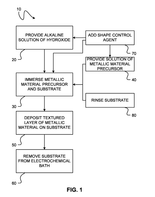
[0113] FIG. 1 shows a method 10 of electrochemical deposition of a textured
layer of a
metallic material on the surface of a substrate. The method involves immersing
a metallic
material precursor and the substrate in an alkaline solution of hydroxide and
depositing a
16
CA 03032224 2019-01-28
WO 2018/018161
PCT/CA2017/050914
textured layer of the metallic material on the surface of the substrate. In
block 20 an
alkaline solution of hydroxide is provided. The solution may be prepared by
dissolving a
hydroxide salt (e.g. sodium hydroxide (NaOH), potassium hydroxide (KOH),
ammonium
hydroxide (NH4OH), etc.) in a liquid. In some embodiments, one or more other
chemical
species may also be dissolved in the liquid. For example, a shape control
agent could be
added to the alkaline solution in optional block 70. To alter the
electrochemical deposition
reaction mechanism and/or the rate of metallic material deposition, one or
more additives
may also be added to the liquid. The additives may interact with one or more
of a cathode
substrate, a layer of a metallic material being deposited on the substrate,
and a complex
comprising an oxidized form of the metallic material precursor. In some
embodiments, the
morphology of the deposited material is influenced by the additive(s).
Examples of
additives include, without limitation, smoothing agents, polishing agents,
etc.
[0114] In some embodiments, the alkaline solution comprises hydroxide and one
or more
other reducing agents. In some embodiments, the concentration of hydroxide
ions in the
.. alkaline solution is greater than about 0.0001 M. In some embodiments, the
concentration
of hydroxide ions in the alkaline solution is between about 0.0001 M and about
10 M. In
some embodiments, the pH of the alkaline solution is greater than about 10. In
some
embodiments, the pH of the alkaline solution is in the range of about 10 to
about 15.
[0115] In block 30 a metallic material precursor and a substrate are immersed
in the
alkaline solution. In some embodiments, the substrate is immersed with the
metallic
material precursor in the alkaline solution. In some embodiments, the
substrate is
immersed before the metallic material precursor is immersed in the alkaline
solution. In
some embodiments, the metallic material precursor is added to the alkaline
solution
continually and/or periodically to maintain the concentration of the metallic
material
.. precursor within a desired range. In some embodiments, immersing the
metallic material
precursor in the alkaline solution before the substrate is immersed may cause
the metallic
material to nucleate, aggregate, agglomerate, precipitate, or otherwise
combine with the
hydroxide and/or the reducing agent to form nanoparticles in the alkaline
solution. Such
nanoparticles can become incorporated into the layer during deposition of the
metallic
.. material onto the substrate, thereby altering the resulting quality and/or
texture of the layer.
However, where the textured layer of the metallic material is deposited on the
surface of the
substrate using electric potential or electric current and the metallic
material precursor is
17
CA 03032224 2019-01-28
WO 2018/018161 PCT/CA2017/050914
provided as a solid anode, the metallic material precursor may be immersed in
the alkaline
solution before, at the same time as, or after the substrate is immersed in
the solution
provided the electrical current is not supplied to the metallic material
precursor until both the
metallic material precursor and the substrate are immersed in the solution. In
some
.. embodiments, immersing the metallic material and the substrate in the
alkaline solution
comprises mixing, agitating, or otherwise stirring the mixture.
[0116] In some embodiments, the substrate comprises a material that is
susceptible to
galvanic replacement in the presence of a metal salt. In some embodiments, the
substrate
need not necessarily be considered to be catalytic for electroless deposition
and may still
.. have a textured layer of the metallic material deposited thereon. In some
embodiments, this
is achieved by rendering the substrate catalytic according to conventional
methods, or by
electroless reduction under conditions that permit galvanic replacement of
substrate surface
atoms, or by other methods that render the substrate suitable for subsequent
electrochemical reduction. Methods of making substrates catalytic are
described in United
.. States patent No. 4,904,506 entitled "Copper Deposition from Electroless
Plating Bath". By
using such methods, electroless deposition onto a range of non-catalytic
substrates may be
accomplished. For example, in some embodiments, the substrate may comprise a
semiconductor (e.g. silicon), an insulator, a polymeric material, etc.
Electrochemical
deposition according to embodiments of the present invention has been observed
using the
.. following substrates: silicon (Si), silver (Ag), gold (Au), platinum (Pt),
palladium (Pd), iridium
(Ir), ruthenium (Ru), copper (Cu), cobalt (Co), steel:copper:nickel alloys,
tin-doped indium
oxide (ITO), glass, polyethylene terephthalate (PET), polyimide (Kapton),
poly(methyl
methacrylate) (PMMA), silicon nitride (Si3N4), silicon oxide (5i02), stannous
chloride
(SnCl2), and palladium chloride (PdC12). Other examples of suitable substrates
include, but
are not limited to, nanoparticles, a suspension of seed nanocrystals, a single-
crystal
substrate, a substantially crystalline substrate, sub-micron apertures formed
on a
substantially crystalline substrate, crystallites formed on a substrate, a
crystalline noble
metal, a crystalline semi-noble metal, etc.
[0117] In some embodiments, the substrate is patterned using a lithographic
process and/or
one or more other patterning methods conventionally known (e.g. wet etching,
dry etching,
etc.). In some embodiments, one or more of subtractive and additive methods
conventionally known are employed to pattern the substrate. Examples of
additive methods
18
CA 03032224 2019-01-28
WO 2018/018161 PCT/CA2017/050914
include, without limitation, electroless deposition, electrodeposition,
physical vapor
deposition, chemical deposition, and atomic layer deposition. Persons skilled
in the art will
recognize that different permutations of the different patterning methods may
be employed
to achieve a desired effect.
[0118] In some embodiments, the metallic material precursor is immersed as a
salt of the
metallic material in block 30. In optional block 40 a solution of the metallic
material
precursor is provided. The solution is prepared by dissolving the metallic
material precursor
(e.g. a metallic material salt) in a liquid. In some embodiments, one or more
other chemical
species may be dissolved in the liquid of the block 40 metallic material
precursor solution.
For example, a shape control agent could be added to the metallic material
solution in
optional block 70. Electrochemical deposition according to embodiments of the
present
invention has been observed using the following metals: gold (Au), silver
(Ag), platinum (Pt),
palladium (Pd), iridium (Ir), rhodium (Rh), copper (Cu), and cobalt (Co).
Other examples of
suitable metals include metals that may have similar chemical properties, but
this is not
necessary.
[0119] The mixture of the alkaline solution and the metallic material
precursor forms an
electrochemical bath. In some embodiments, the concentration of metal ions
dissolved in
the electrochemical bath may be between about 1 x 10⁻⁷ M and about 1 M, or the
maximum
allowable concentration dictated by metallic material precursor solubility. A
person skilled in
the art would understand that the concentration of the metallic material
precursor and the
reducing agent (i.e. hydroxide with or without other reducing agents) in the
electrochemical
bath depends on: (i) the concentration of the reducing agent in the alkaline
solution; (ii) the
concentration of the metallic material precursor in the metallic material
solution; (iii) the
volume of the alkaline solution; and (iv) the volume of the metallic material
solution added to
the alkaline solution. In some embodiments, the concentration of hydroxide
ions in the
electrochemical bath is between about 0.0001 M and about 15 M. In some
embodiments,
the pH of the electrochemical bath is greater than about 10. In some
embodiments, the pH
of the electrochemical bath in the range of about 10 to about 15. In some
embodiments, the
pH of the electrochemical bath is about 10. In some embodiments, the pH of the
electrochemical bath is about 11. In some embodiments, the pH of the
electrochemical
bath is about 12. In some embodiments, the pH of the electrochemical bath is
about 13. In
19
CA 03032224 2019-01-28
WO 2018/018161
PCT/CA2017/050914
some embodiments, the pH of the electrochemical bath is about 14. In some
embodiments,
the pH of the electrochemical bath is about 15.
[0120] For example, to deposit a textured layer of the metallic material on a
single-crystal
silver substrate (e.g. Ag (100)) having a surface area of about 1 cm2 (i.e.
about 1 cm by
about 1 cm), the electrochemical bath may comprise the following
concentrations of metal
ions and hydroxide ions:
Metal ion concentration (M) Hydroxide ion concentration (M)
about 10-5 M - about 10-1 M about 0.1 M - about 10 M
about 10-4 M - about 7.5 x 10⁻² M about 0.5 M ¨ about 8.0 M
about 10-3 M - about 5 x 10⁻² M about 0.5 M - about 4.0 M
[0121] In some embodiments, the ratio of hydroxide ion concentration:metal ion
concentration in the electrochemical bath is greater than about 400:1 when the
substrate is
susceptible to galvanic replacement in the presence of the metallic material
precursor. In
some embodiments, the ratio of the concentration of the hydroxide ions to the
concentration
of the metallic material precursor in the electrochemical bath is in the range
of about 50:1 to
about 400:1 when the substrate is not susceptible to galvanic replacement in
the presence
of the metallic material precursor. In some embodiments, the ratio of the
concentration of
the hydroxide ions to the concentration of the metallic material precursor in
the
electrochemical bath is greater than about 50:1 when the substrate is not
susceptible to
oxidation in the presence of the metallic material precursor.
[0122] In block 50 a textured layer of the metallic material is deposited on
the surface of the
substrate via electrochemical deposition. In some embodiments, it is desirable
to maintain
uniform kinetics of deposition. To do so, the concentration of one or more of
the metal ion
and the hydroxide ion may be monitored during the deposition period, or a
portion thereof.
Information regarding the rate of deposition may be monitored through optical
absorption
properties of the electrochemical bath when the metal ions in the bath have
spectral
characteristics that allow them to be detected using conventional methods
(e.g. optical
absorbance at characteristic wavelengths). The kinetics of deposition may be
estimated
based on the rate at which the metal ions leave the electrochemical bath (i.e.
are deposited
on the substrate). In some embodiments, a syringe pump may be used to add one
or more
CA 03032224 2019-01-28
WO 2018/018161 PCT/CA2017/050914
of the metal ion and the hydroxide ion at a continual rate or periodically to
maintain uniform
kinetics of deposition.
[0123] In some embodiments, the textured layer is a metal alloy.
Electrochemical
deposition according to some embodiments of the present invention has been
observed
using the following metal alloys: gold (Au) and silver (Ag), platinum (Pt) and
silver (Ag),
platinum (Pt) and gold (Au), palladium (Pd) and silver (Ag), palladium (Pd)
and gold (Au),
cobalt (Co) and gold (Au), cobalt (Co) and copper (Cu), copper (Cu) and gold
(Au), copper
(Cu) and platinum (Pt), and a four member alloy consisting of copper (Cu),
gold (Au), silver
(Ag), and cobalt (Co). Other examples of suitable metal alloys may have
similar chemical
properties, but this is not necessary. FIG. 2C is a schematic illustration of
a single-crystal
substrate 110 upon which a metal alloy 140 has been deposited. Film colour was
considered evidence of alloying. Also, scanning electron microscopy (SEM) was
used to
show surface morphology of the deposited layers and to distinguish between
uniform
deposition from electrochemical baths containing mixtures of metallic material
precursors
and metallic phase separation. X-ray diffraction (XRD) and X-ray photoelectron
spectroscopy (XPS) were used to confirm the electrochemical deposition of the
following
alloys: Au:Ag, Pt:Ag, and Pt:Au.
[0124] In block 40 two or more metallic material precursors may be dissolved
in the liquid.
For example, to deposit a platinum-silver alloy layer, a platinum salt and a
silver salt are
.. dissolved in the liquid. To deposit a platinum-gold alloy, a platinum salt
and a gold salt (e.g.
HAuC14) are dissolved in the liquid. To deposit a platinum-palladium alloy, a
platinum salt
and a palladium salt are dissolved in the liquid. Due to such factors as
different reduction
potentials, the number of electrons required for reduction, different
concentrations, etc., the
concentrations of the different metal salts in the metallic material solution
(and in the
electrochemical bath) may not accurately reflect the alloy composition of the
layer that is
eventually deposited. The composition of the deposited layer may be analyzed
using
conventional analytical methods. Information regarding the relative rates of
deposition of
the different metal ions may also be monitored through optical absorption
properties of the
electrochemical bath when the metal ions in the bath have spectral
characteristics that allow
them to be detected using conventional methods (e.g. optical absorbance at
characteristic
wavelengths). The kinetics of deposition and alloy composition may be
estimated based on
the rate at which the metal ions leave the electrochemical bath (i.e. are
deposited on the
21
CA 03032224 2019-01-28
WO 2018/018161
PCT/CA2017/050914
substrate). Where the kinetics of deposition of the different metal ions
differ significantly, to
maintain uniform alloy composition throughout the deposited layer, the
concentration of
each metal ion may be maintained within the ranges outlined elsewhere herein
during the
deposition period.
[0125] In some embodiments, the textured layer deposited in block 50 is a
metal-containing
compound. Electrochemical deposition according to embodiments of the present
invention
has been observed to deposit copper oxide (Cu2O) and cobalt monoxide (Co0).
Other
examples of suitable metal-containing compounds may have similar chemical
properties,
but this is not necessary. For example, the textured layer may comprise
aluminum oxide
(A1203), zinc oxide (Zn0), etc.
[0126] In some embodiments, to deposit the metallic material on the substrate
via
electrodeposition, an external electric potential or electric current is
supplied to the
electrochemical bath in block 50. In some embodiments, the metallic material
is deposited
on the surface of the substrate in a non-galvanic process, without the use of
external
electric potential or electric current (i.e. via electroless deposition). In
some embodiments,
electromagnetic radiation is used in block 50 to deposit the metallic material
on the
substrate via photoelectrochemical deposition. In some embodiments, the
wavelengths of
the electromagnetic radiation correspond with those capable of forming an
excitation. Such
excitation may include, but are not limited to, one or more of excitons,
polarons, bipolarons,
polaritons, plasmons, surface plasmon polaritons (SPPs), locally resonant
surface
plasmons (LRSPs), photothermal excitations, and/or other excitations,
including those that
lead to electron generation directly, or that can lead to direct or indirect
reduction of ionic
species. By way of non-limiting example, FIG. 3A shows a schematic
illustration of a
substantially crystalline substrate 310 upon which a LRSP active element 320
is deposited.
Electromagnetic radiation 325 is radiated onto the surface of substrate 310.
By way of non-
limiting example, FIG. 3B shows a schematic illustration of a substantially
crystalline
substrate 330 upon which LRSP-mediated reduction on LRSP active elements 340
and
LRSP active elements 350 are deposited.
[0127] In some embodiments, the wavelengths of the electromagnetic radiation
are
between Angstroms and meters. The electromagnetic radiation may induce
excitations and
ultimately result in reduction through interaction of the electromagnetic
radiation with one or
22
CA 03032224 2019-01-28
WO 2018/018161 PCT/CA2017/050914
more of the substrate, chemical species supported on the substrate (e.g. shape
control
agent(s), etc.), and components of the electrochemical bath.
[0128] Without being bound by theory, the inventors consider that the
concentration of
hydroxide and/or the alkaline pH of the reducing agent solution facilitates
electrochemical
reduction of the metallic material precursor while preventing galvanic
replacement or other
deleterious oxidation processes that can occur to the substrate in less
alkaline
environments and/or environments with lower concentrations of hydroxide. In
some
embodiments, the concentration of hydroxide in the electrochemical bath is
sufficient so that
hydroxide acts as the reducing agent. In some embodiments, the electrochemical
bath
comprises one or more other reducing agents in addition to hydroxide.
[0129] Electrochemical deposition may be achieved at room temperature. In some
embodiments, the temperature of the electrochemical bath is controlled in
block 50. For
example, temperature may be maintained in the range of about 5 C to about 90
C. In some
embodiments, the temperature is maintained in the range of about 50 C to about
80 C. In
some embodiments, the temperature is maintained at about 70 C. In some
embodiments,
the temperature is varied in block 50. In some embodiments, the temperature of
the
alkaline solution and/or the metallic metal solution is controlled. In some
embodiments, the
electrochemical bath is formed at room temperature and then heated to achieve
a desired
temperature. In some embodiments, the electrochemical bath is formed at the
desired
temperature. The temperature may be controlled using any means conventionally
known.
[0130] After a time sufficient to achieve the desired thickness of metallic
material deposited
on the surface of the substrate, the substrate is removed from the
electrochemical bath in
block 60. Depending on the desired thickness, the deposition is carried out
for a period of
time between minutes to hours. For example, in some embodiments, to achieve a
deposited textured layer thickness of about 70 to about 100 nm, about 0.5
hours to about 5
hours of deposition may be required. In some embodiments, a similar thickness
may be
achieved in about 1 hour or less. Once removed, the substrate may be rinsed
with a liquid
to cease electrochemical deposition. In some embodiments, deposition may be
reduced or
terminated in block 60 by removing the current and/or electromagnetic
radiation supplied to
the metallic material precursor. Layer thickness and/or quality may be
optimized by varying
one or more of the following: (i) deposition time; (ii) temperature; (iii)
concentration of the
metallic material precursor in the electrochemical bath; (iv) concentration of
the hydroxide
23
CA 03032224 2019-01-28
WO 2018/018161
PCT/CA2017/050914
ions in the electrochemical bath; (v) surface area of the substrate; (vi) type
of substrate (for
example, without limitation, the relative reduction potential of the
substrate); (vii) type of
metallic material (for example, without limitation, the required number of
electrons for
reduction of a particular ionic species, the relative reduction potential,
etc.); and (viii)
concentration of reducing agent(s) other than hydroxide in the electrochemical
bath.
[0131] In some embodiments, to achieve the deposit of a textured layer of
metallic material
on the substrate, the concentration of the metallic material precursor in the
electrochemical
bath must be maintained at desired levels, wherein these concentration levels
typically
depend on the specific application. For example, to form a textured layer of a
metallic
material on a substantially crystalline substrate (e.g. a Ag(100) single-
crystal surface), the
concentration of metal ions in the electrochemical bath may be maintained at a
sufficiently
low concentration to avoid substrate oxidation (if the substrate is capable of
oxidizing)
and/or to avoid excessive formation of nanocrystals. Such nanocrystals can
aggregate,
agglomerate, precipitate, or otherwise become incorporated into the layer
during deposition
and alter the quality of the layer. If the concentration of the metallic
material precursor is
too high and excessive formation of nanocrystals results, the deposited layer
may become
polycrystalline and/or porous. However, in some applications, a
polycrystalline and/or
porous deposited layer is desirable. Accordingly, method 10 may be optimized
to yield a
desired morphology of the deposited layer of a metallic material. In some
embodiments, it
is desirable to form nanocrystals. To do so, the concentration of the metal
ions in the
electrochemical bath may be maintained at a sufficiently high concentration to
induce
formation of nanocrystals.
[0132] In some embodiments, to achieve the deposit of a textured layer of
metallic material
on the substrate, the concentration of the hydroxide ions in the
electrochemical bath is
maintained at desired levels, wherein these concentration levels depend on the
specific
application. Other conventional electroless deposition processes employ
specific reducing
agents in less alkaline environments. However, many of these methods are
unable to
prevent unwanted oxidative processes from compromising the integrity of the
substrate
and/or are unable to achieve the deposit of an epitaxial layer of a metallic
material on a
substrate. For example, the electroless deposition of gold (Au) onto silver
(Ag) is well
known. Due to the higher reduction potential of Au3+ ions compared to Ag+
ions, gold is
reduced at the expense of silver oxidation. This results in a highly porous Au
or Au/Ag
24
CA 03032224 2019-01-28
WO 2018/018161 PCT/CA2017/050914
composite deposition layer. As a result, many commercially significant gold
plating
applications are carried out using electrodeposition processes.
[0133] The inventors have found that depositing gold onto silver according to
some
embodiments of the present invention avoids deleterious silver oxidation.
Without being
bound by theory, the inventors consider that at appropriately high hydroxide
ion
concentrations and/or alkaline pH, gold ions form complexes with hydroxide
ions and that
the kinetic rate of gold ion reduction by the hydroxide ions is greater than
the kinetic rate of
gold ion reduction by silver oxidation. The concentration of hydroxide and/or
the alkaline pH
of the electrochemical bath may facilitate electrochemical reduction of the
metallic material
precursor while preventing galvanic replacement or other deleterious oxidation
processes
that can occur to the substrate in less alkaline environments and/or
environments with lower
concentrations of hydroxide. The inventors have found that depositing gold
onto silver
according to some embodiments of the present invention avoids deleterious
silver oxidation
and produces a textured layer of gold deposited onto the silver. Sufficiently
high
concentrations of hydroxide (as described elsewhere herein) and/or alkaline pH
may also
be beneficial for the deposition of other metallic materials that are not
capable of
undergoing galvanic replacement and/or for the deposition of metallic
materials on
substrates that are not capable of undergoing galvanic replacement.
[0134] In some embodiments, the rate of electrochemical deposition is
controlled. For
.. example, in optional block 80 the rate may be enhanced by rinsing the
substrate with a
liquid before immersing the substrate in the alkaline solution. In some
embodiments, the
substrate is rinsed with an alcohol. In some embodiments, the substrate is
rinsed with
isopropyl alcohol. In some embodiments, the substrate is rinsed with a
solution of water
and an alcohol. To deposit a layer of metallic material having a desired
thickness, a
deposition period of about 5 minutes to about 10 minutes was observed when the
substrate
was rinsed with isopropyl alcohol before immersing the substrate in the
alkaline solution.
To deposit a layer of metallic material having the same thickness on a
substrate that was
not rinsed prior to being immersed in the alkaline solution, a deposition
period of about 1
hour was required.
[0135] The layer of metallic material deposited according to method 10 may be
textured. In
some embodiments, the textured layer is epitaxial. For example, the
electroless deposition
of a metallic material on a single-crystal silver (Ag(100)) substrate
according to method 10
CA 03032224 2019-01-28
WO 2018/018161 PCT/CA2017/050914
was observed to yield an epitaxial layer of the metallic material deposited on
the surface of
the substrate. FIG. 2A is a schematic illustration of a crystalline epitaxial
layer 100 of
metallic material deposited on a single-crystal Ag substrate 110. The
distribution of
crystallographic orientations of the deposited textured layer of metallic
material may depend
on the geometry and/or texture of the substrate to be plated. In some
embodiments, the
distribution of crystallographic orientations of the deposited textured layer
of metallic
material reflects the geometry and/or texture of the substrate to be plated.
For example, the
electroless deposition of a metallic material on an amorphous substrate
according to
method 10 was observed to yield an amorphous layer of the metallic material
deposited on
the surface of the substrate. The electroless deposition of a metallic
material on a
polycrystalline substrate according to method 10 was observed to yield a
polycrystalline
layer of the metallic material deposited on the surface of the substrate (see
also FIG. 28A
and 28B). In some embodiments, deposition of a metallic material according to
method 10
on a polycrystalline substrate containing voids leads to deposition of a layer
with fewer
voids and a more continuous character, thereby demonstrating film healing
properties.
[0136] To deposit a textured layer of metallic material having a preferred
geometry and/or
morphology and/or crystalline composition, one or more shape control agents
may be used.
In optional block 70 one or more shape control agents are provided. The shape
control
agent(s) may impart differential growth kinetics and, in some embodiments,
result in
crystalline deposits with crystallographic texture and/or well-defined shape
preferences.
Such crystalline qualities cannot typically be achieved using conventional
electroless
deposition without such shape control agents. One or more shape control agents
may be
added to one or more of the alkaline solution (in block 20), the metallic
material solution (in
block 40), and the electrochemical bath (in block 30). By way of non-limiting
example, FIG.
4A shows a schematic illustration of a variety of shaped crystallites 220
supported by a
substantially crystalline substrate 230. By way of non-limiting example, FIG.
4B shows a
schematic illustration of an epitaxial layer 240 of a metallic material
deposited on the FIG.
4A shaped crystallites 220 and substrate 230. By way of non-limiting example,
FIG. 5A
shows a schematic illustration of a shape-controlled epitaxy 250 demonstrating
homoepitaxial deposition of square pyramidal crystallites 260 onto a patterned
substrate
270 (i.e. additive deposition). By way of non-limiting example, FIG. 5B shows
a schematic
26
CA 03032224 2019-01-28
WO 2018/018161
PCT/CA2017/050914
illustration of a shape-controlled epitaxy 280 demonstrating heteroepitaxial
deposition of
cubic crystallites 290 onto a patterned substrate 300.
[0137] In some embodiments, the plated substrate may be further processed by
one or
more of: electrodeposition, chemical vapor deposition, physical vapor
deposition, and
atomic layer deposition. In some embodiments, the plated substrate may be
patterned
using a lithographic process and/or one or more other patterning methods
conventionally
known (e.g. wet etching, dry etching, etc.). In some embodiments, one or more
of
subtractive and additive methods conventionally known are employed to pattern
the plated
substrate. In some embodiments, one or more layers of a metallic material may
be
deposited on a substrate. For example, FIG. 2B is a schematic illustration of
a single-
crystal substrate 110 coated with two crystalline epitaxial layers 120, 130 of
metallic
materials. Persons skilled in the art will recognize that many different
permutations of the
different deposition and/or patterning methods may be employed to achieve a
desired
effect.
[0138] FIG. 6A shows a method 400 of making textured nanoparticles via
electrochemical
deposition. Unlike method 10, method 400 involves forming nanoparticles by
electrochemical deposition and then either depositing the nanoparticles onto a
substrate or
removing the nanoparticles from the solution and optionally depositing a
metallic material
onto the nanoparticles. Method 400 comprises immersing a metallic material
precursor in
an alkaline solution of hydroxide. In block 410 an alkaline solution of
hydroxide is provided.
The block 410 solution may be prepared by using techniques described for block
20. A
shape control agent may be added to the block 410 alkaline solution in
optional block 420
as described for block 70.
[0139] In some embodiments, the alkaline solution comprises hydroxide and one
or more
other reducing agents. In some embodiments, the concentration of hydroxide
ions in the
alkaline solution is greater than about 0.0001 M. In some embodiments, the
concentration
of hydroxide ions in the alkaline solution is between about 0.0001 M and about
15 M. In
some embodiments, the pH of the alkaline solution is greater than about 10. In
some
embodiments, the pH of the alkaline solution is in the range of about 10 to
about 15.
[0140] In block 430 a metallic material precursor is immersed in the alkaline
solution. In
some embodiments, the metallic material precursor may be added to the alkaline
solution
27
CA 03032224 2019-01-28
WO 2018/018161
PCT/CA2017/050914
continually and/or periodically to maintain the concentration of the metallic
material
precursor within a desired range. In some embodiments, the metallic material
precursor is
immersed as a salt of the metallic material in block 430. In optional block
440 a solution of
a salt of the metallic material is provided as described for block 40. A shape
control agent
could be added to the metallic material solution in optional block 420.
[0141] The mixture of the alkaline solution and the metallic material
precursor forms an
electrochemical bath. In some embodiments, the concentration of metal ions
dissolved in
the electrochemical bath may be between about 1 x 10⁻⁷ M and about 1 M, or the
maximum
allowable concentration dictated by metallic material precursor solubility. In
some
embodiments, the concentration of hydroxide ions in the electrochemical bath
is between
about 0.0001 M and about 15 M. In some embodiments, the pH of the
electrochemical bath
is greater than about 10. In some embodiments, the pH of the electrochemical
bath in the
range of about 10 to about 15. In some embodiments, the pH of the
electrochemical bath is
about 10. In some embodiments, the pH of the electrochemical bath is about 11.
In some
embodiments, the pH of the electrochemical bath is about 12. In some
embodiments, the
pH of the electrochemical bath is about 13. In some embodiments, the pH of the
electrochemical bath is about 14. In some embodiments, the pH of the
electrochemical
bath is about 15.
[0142] In some embodiments, the ratio of hydroxide ion concentration:metal ion
concentration in the electrochemical bath is greater than about 400:1 when the
substrate is
susceptible to galvanic replacement in the presence of the metallic material
precursor. In
some embodiments, the ratio of the concentration of the hydroxide ions to the
concentration
of the metallic material precursor in the electrochemical bath is in the range
of about 50:1 to
about 400:1 when the substrate is not susceptible to galvanic replacement in
the presence
of the metallic material precursor. In some embodiments, the ratio of the
concentration of
the hydroxide ions to the concentration of the metallic material precursor in
the
electrochemical bath is greater than about 50:1 when the substrate is not
susceptible to
oxidation in the presence of the metallic material precursor.
[0143] Immersing the metallic material precursor in the alkaline solution in
block 430 may
cause the metallic material to nucleate, aggregate, agglomerate, or otherwise
combine with
the hydroxide and/or the reducing agent to form crystalline nanoparticles in
the alkaline
solution in block 435. The formed nanoparticles may be deposited onto a
substrate by
28
CA 03032224 2019-01-28
WO 2018/018161 PCT/CA2017/050914
following path 445, 455. To deposit the nanoparticles onto a substrate, the
substrate is
immersed in the electrochemical bath in optional block 450. In block 460, the
nanoparticles
are incorporated into a layer of metallic material deposited on a substrate
via
electrochemical deposition to alter the quality and/or texture of the
deposited layer.
[0144] Alternatively, the formed nanoparticles may be removed from solution
and optionally
plated with a metallic material by following path 475. In optional block 470,
the
nanoparticles may be removed from the electrochemical bath. A metallic
material may be
deposited on the nanoparticles via electrochemical deposition in optional
block 480 10 to
produce core-shell nanoparticles having a textured shell. In some embodiments,
the
metallic material is deposited according to method 10 to produce core-shell
nanoparticles
having a textured shell.
[0145] In some embodiments, a layer of a metallic material is deposited on
nanoparticles
formed independently of method 400 to produce core-shell nanoparticles
comprising a
textured shell. For example, FIG. 6B shows a method 500 of making core-shell
nanoparticles having a textured shell via electrochemical deposition. The
method involves
immersing a metallic material precursor in an alkaline solution of hydroxide.
In block 510 an
alkaline solution of hydroxide is provided. The solution is prepared by as
described for
block 20.
[0146] In some embodiments, the alkaline solution comprises hydroxide and one
or more
other reducing agents. In some embodiments, the concentration of hydroxide
ions in the
alkaline solution is greater than about 0.0001 M. In some embodiments, the
concentration
of hydroxide ions in the alkaline solution is between about 0.0001 M and about
15 M. In
some embodiments, the pH of the alkaline solution is greater than about 10. In
some
embodiments, the pH of the alkaline solution is in the range of about 10 to
about 15.
[0147] In block 530 a metallic material is immersed in the alkaline solution.
In some
embodiments, the metallic material precursor is added to the alkaline solution
continually
and/or periodically to maintain the concentration of the metallic material
precursor within a
desired range. In some embodiments, the metallic material precursor is
immersed as a
salt of the metallic material in block 530. In optional block 540 a solution
of a salt of the
.. metallic material is provided as described for block 40.
29
CA 03032224 2019-01-28
WO 2018/018161
PCT/CA2017/050914
[0148] The mixture of the alkaline solution and the metallic material
precursor forms an
electrochemical bath. In some embodiments, the concentration of metal ions
dissolved in
the electrochemical bath may be between about 1 x 10⁻⁷ M and about 1 M, or the
maximum
allowable concentration dictated by metallic material precursor solubility. In
some
embodiments, the concentration of hydroxide ions in the electrochemical bath
is between
about 0.0001 M and about 15 M. In some embodiments, the pH of the
electrochemical bath
is greater than about 10. In some embodiments, the pH of the electrochemical
bath in the
range of about 10 to about 15. In some embodiments, the pH of the
electrochemical bath is
about 10. In some embodiments, the pH of the electrochemical bath is about 11.
In some
embodiments, the pH of the electrochemical bath is about 12. In some
embodiments, the
pH of the electrochemical bath is about 13. In some embodiments, the pH of the
electrochemical bath is about 14. In some embodiments, the pH of the
electrochemical
bath is about 15.
[0149] In some embodiments, the ratio of hydroxide ion concentration:metal ion
concentration in the electrochemical bath is greater than about 400:1 when the
substrate is
susceptible to galvanic replacement in the presence of the metallic material
precursor. In
some embodiments, the ratio of the concentration of the hydroxide ions to the
concentration
of the metallic material precursor in the electrochemical bath is in the range
of about 50:1 to
about 400:1 when the substrate is not susceptible to galvanic replacement in
the presence
of the metallic material precursor. In some embodiments, the ratio of the
concentration of
the hydroxide ions to the concentration of the metallic material precursor in
the
electrochemical bath is greater than about 50:1 when the substrate is not
susceptible to
oxidation in the presence of the metallic material precursor.
[0150] In block 520 nanoparticles are added to one or more of the alkaline
solution, the
metallic material precursor solution, and the electrochemical bath.
[0151] In block 550, a layer of a metallic material is deposited on the
nanoparticles via the
electrochemical deposition method 10 to produce core-shell nanoparticles
having a textured
shell.
[0152] Conventional methods of electrochemical deposition of a metallic
material on a
single-crystal substrate result in polycrystalline or amorphous material
deposition. Because
of losses due to grain boundaries and defects, such materials typically have
poor
CA 03032224 2019-01-28
WO 2018/018161 PCT/CA2017/050914
performance characteristics and compromised thermal and mechanical
stabilities. For
example, the resistivity of a material is known to increase as a result of
imperfections, such
as defects, impurities, grain boundaries, and dislocations (see Ziman, J.M.
"Electrons and
Phonons", Clarendon Press, Oxford, 1960). The increased resistance and thermal
loading
associated with charge transport through polycrystalline material can be
mitigated by
reducing or eliminating the number of grain boundaries within the material.
For example,
single-crystal copper has better conductivity than polycrystalline copper.
Accordingly,
epitaxial metallic material deposition according to some embodiments of the
present
invention may mitigate charge transport loss across interfaces. The absence of
the defects
associated with grain boundaries in thin film and bulk materials may also give
unique
properties, particularly mechanical, optical, electrical and magnetic, which
can also be
anisotropic, depending on the type of crystallographic structure of the
textured metallic
material.
[0153] The use of single-crystal metallic materials to create plasmonic
structures and meta-
materials is anticipated to minimize optical losses originating from grain
boundaries and
surface roughness, demonstrate improved mechanical and thermal stability of
nanostructures, provide enhanced localized surface plasmon resonant (LSPR)
field intensity
of well-faceted nanostructured elements, and generate enhanced plasmonic
coupling
between high definition nanoscale features. For example, single-crystal silver
films sputter
deposited on Si(111) substrates have been patterned by electron beam
lithography and
plasma etching to yield visible frequency hyberbolic metasurfaces that display
the
characteristic properties of metamaterials with device performance greatly
exceeding
previous demonstrations with polycrystalline silver films (see, for example,
Kildishev, A.V.,
Boltasseva, A., Shalaev, V.M. "Planar photonics with metasurfaces", Science,
2013: 339
(1232009); Liu, Y.M., Zhang, X. "Metasurfaces for manipulating surface
plasmons", Appl.
Phys. Lett. 2013: 103 (141101); High, A. A., Devlin, A.A., Dibos, A., Polking,
M., Wild, D.S.,
Perczel, J., de Leon, N.P., Lukin, M.D., Park, H. "Visible-frequency
hyperbolic metasurface",
Nature, 2015(522):192.) Other plasmonic applications as described by Leach et
al. in
United States patent application No. 13/813,143 entitled "Apparatus for
Manipulating
Plasmons" and metamaterial applications (see, for example, Pendry, J.B.
"Negative
refraction makes a perfect lens". Phys. Rev. Lett. 2000(85): 3966) may benefit
from
patterned features which are crystalline and epitaxially deposited.
31
CA 03032224 2019-01-28
WO 2018/018161 PCT/CA2017/050914
[0154] Many beam steering applications in X-ray optics and X-ray microscopy
rely on
optical elements that are based on diffractive effects rather than refractive
effects. The
beam steering and imaging quality of these optical elements are determined by
their
diffraction efficiencies at relevant X-ray wavelengths. They are typically
fabricated from
metals such as gold because of its high electron density and ease of
fabrication (e.g.
electroplating) (see, for example, Anderson, E.H., Olynick, D.L., Harteneck,
B., Veklerov, E.,
Denbeaux, G., Chao, W., Lucero, A., Johnson, L., and Attwood, D.
"Nanofabrication and
diffractive optics for high-resolution x-ray applications", J. Vac. Sci.
Technol. B, 2000(18): 6;
Jefimovs, K., Bunk, 0., Pfeiffer, F., Grolimund, D., van der Veen, J.F. David,
C. "Fabrication
of Fresnel zone plates for hard X-rays", Microelectronic Engineering, 2007
(84): 1467-
1470). However, the optimal thicknesses of metal features in these structures
cannot be
achieved readily and are limited by technical difficulties in attaining high
quality, high aspect
ratio metal deposition. Improving the diffraction efficiency by increasing the
aspect ratio of
lithographed metal features and/or improving the diffraction efficiency of the
deposited
metallic material may lead to improved performance of the optical elements.
Current
fabrication methods that employ electroplating of Au into lithographed
structures such as
zone plates, lead to polycrystalline Au deposition with lower diffraction
efficiencies than
those expected from single-crystal Au deposition. The ability to deposit
highly crystalline
metallic materials into high aspect ratio features may lead to improved
diffraction efficiency
and mitigate the requirement for deposition of even higher aspect ratio
structures
associated with polycrystalline metal deposition.
[0155] The use of metal and metal alloys to catalyze chemical reactions is
well known.
Metal catalyst materials such as platinum (Pt) and Pt alloys, for example, are
known to be
some of the most effective catalyst materials for oxygen reduction reactions
(ORR) and
hydrogen evolution reactions (HER). Such reactions are important to hydrogen
fuel cell
technologies and producing H2 for clean energy applications, respectively.
Improving a
catalyst's activity and/or stability can reduce its loading requirements and
improve the
efficiency of a technology while reducing production costs, particularly when
the catalyst is
an expensive and rare element (e.g. Pt). Metal catalysts can assist in
transferring electrons
to reactants and/or alter their energetics and/or facilitate an intermediate
chemical
transformation. The ability of a catalyst to act in one or more of these ways
is recognized to
be dependent on the crystallinity of the catalyst material, with some crystal
facets leading to
32
CA 03032224 2019-01-28
WO 2018/018161
PCT/CA2017/050914
enhanced catalytic performance over others. The use of catalyst alloys can
alter energetics
and/or bond lengths, leading to improved catalytic activity and/or stability.
The ability to
deposit a catalyst material as an element, compound, or alloy in an epitaxial
manner may
enable the creation of catalysts with preferential faceting and enhanced
catalytic activity.
Epitaxial crystalline deposition of catalyst materials may also enable higher
mechanical
and/or thermal and/or chemical stability, thereby improving catalyst
longevity.
[0156] Other applications where materials are patterned or lithographed may
also benefit
from epitaxial and crystalline deposition. The magnetic properties of metals
and their alloys
are dependent on their crystallinity, grain size, and relative orientation.
The ability to
fabricate higher density magnetic storage media is limited by the magnetic
anisotropy of
single lithographed bits, which typically comprise multiple grains of material
(e.g. PtCo
alloy). While efforts to shrink the bit and grain sizes have led to
significant increases in
storage density, further grain size reduction is anticipated to be limited by
thermal instability,
even at room temperature. The energy required to reverse the magnetization of
a magnetic
region is proportional to the size of the magnetic region and the magnetic
coercivity of the
material. If the grains are very small, there may be enough thermal energy to
reverse the
magnetization in a region of the medium, comprising the stored data.
Increasing the
magnetic anisotropy of the grains would allow for higher thermal stability,
smaller grains,
and higher storage density. Current efforts to overcome these limits include
moving to new
materials with higher coercivity, although this is accompanied by other
technological
challenges. Alternatively, bit patterned media is another strategy to enhance
storage
density in which one can record data in magnetic islands (one bit per island).
The islands
would be patterned from a precursor magnetic film using nanolithography. This
approach
also has several technological hurdles associated with it. It is anticipated
that the ability to
deposit epitaxial, crystalline magnetic films may provide a means to control
the
magnetocrystalline and/or stress and/or shape anisotropies. This may provide
the
opportunity for an increase in the effective magnetic anisotropy and/or
smaller bit size
and/or higher storage density, independent of magnetic storage strategy.
[0157] Another potential application related to some embodiments of the
present invention
includes the formation of optical variable devices (OVD) comprising periodic
and/or
aperiodic arrays of shape-specific structures for security applications. As
described in
United States patent application publication No. 2015/0347887 entitled
"Optically Variable
33
CA 03032224 2019-01-28
WO 2018/018161 PCT/CA2017/050914
Data Storage Device", such structures will have very specific optical
signatures which are
directly related to both the shape and the formation of these structures, as
well as the
orientation of these features with respect to each other. In the case of an
OVD using
plasmonic materials, the opto-plasmonic responses of such an OVD can be
controlled and
defined by the shape of the structures made from one or a combination of
several
plasmonic materials. When the variations in optical or opto-plasmonic response
can be
measured with an appropriate reading device which is capable of detecting the
optical
signatures, such an OVD may be used in applications that involve security and
authentication, and may be used as an overt and covert security device. Such
technology
may benefit from a plurality of physical signatures to enhance the level of
security by
incorporating both optical and other responses (e.g. magnetic response). This
technology
may benefit from the use of high quality crystalline structures and further,
from such
structures that display shape preference to generate more well defined optical
and/or other
physical response.
[0158] Printed electronics refers to the use of printing methods to create
electrical devices
on various substrates. As opposed to conventional electronic devices that are
fabricated
with high integration density on rigid substrates using sophisticated
patterning and
fabrication techniques that are typically high cost, printed electronics
employs simple and
extremely low cost fabrication methods to pattern substrates, including
flexible substrates,
over large area with comparatively low integration density. A key element of
this technology
is the ink which desirably enables electrical conduction. One of the primary
printed
electronics strategies involves the use of inks that contain silver nanowires
or other
conducting elements. However, the resulting printed circuit elements can
possess less-
than-desired conductivity characteristics, including, for example, when their
substrates are
subjected to stress and strain that can accompany flexure, or via oxidation of
the circuit
elements. This printed electronics technology may benefit from embodiments of
the present
invention by improving the quality of conduction of printed circuit elements
through the
deposition of conducting metals that contain fewer voids and grain boundaries
and/or are
less subject to oxidation. Circuit elements comprising continuous metal, as
opposed to inks
containing dispersions of metallic components, may preserve desirable
conduction
characteristics under conditions of more severe mechanical deformation.
34
CA 03032224 2019-01-28
WO 2018/018161 PCT/CA2017/050914
[0159] Another potential area of application of embodiments of the present
invention
involves the fabrication of transparent conducting substrates. Such substrates
are desirable
for many technologies that involve the transmission of light as well as the
conduction of
electric charge. Examples include, without limitation, electrochromic windows
and optical
light emitting diodes (OLEDs). Transparent conducting substrates in current
use typically
comprise glass or other transparent material covered with a polycrystalline
film of doped
oxide (e.g. tin-doped indium oxide or indium tin oxide (ITO)). The high band
gap oxide
results in transparency in the optical region of the spectrum, while doping
imparts limited
conductivity. Improved conductivity comes with increasing film thickness, but
increasing
optical absorbance associated with the dopant induced free charge carriers as
well,
resulting in a trade-off between conductivity and transparency. Embodiments of
the present
invention may allow deposition of highly conductive metals with controlled
thickness. In
cases where the metal deposited does not interfere with the optical properties
of the
resultant device, or where very thin layers that may not adversely affect the
optical
properties of the device, embodiments of the present invention may offer a
method to
provide high conductivity on transparent or partially transparent substrates
with beneficial
conductivity.
Example 1 ¨ Epitaxial Electroless Deposition of Au(100) on Planar Ag(100)
[0160] Electroless deposition was carried out on a single-crystal silver
(Ag(100) substrate of
area 1 cm x 1 cm according to method 10 of FIG. 1. The substrate was immersed
in a 1.0
M aqueous solution of NaOH. 500 pL of 0.0025 M of HAuCI4 salt(ac) was then
added to 10
mL of 1.0M NaOH(ac) and the substrate was immersed in the resulting
electrochemical bath
for 2 hours. The temperature of the electrochemical bath was maintained at 60
C during
the deposition period. The resulting layer of gold deposited on the silver
substrate was
about 70 nm in thickness. The layer was observed to be an epitaxial Au(100)
film (see
FIGS. 8-11). No oxidation of the silver substrate was observed. Accordingly,
these
conditions produced an epitaxial gold layer on the Ag(100) substrate in the
absence of the
deleterious effects of galvanic replacement.
Example 2 ¨ Characterization of Film Quality
[0161] The quality of a metallic material layer deposited according to method
10 of FIG. 1
was assessed using conventional physical characterization methods, including X-
ray
CA 03032224 2019-01-28
WO 2018/018161 PCT/CA2017/050914
diffraction and electron microscopy. To compare the quality of various films,
the metallic
material was deposited on a highly uniform, ultra-flat (i.e. single-crystal)
substrate. The
least crystalline form of a film (i.e. a powder) comprises many randomly
ordered crystallites.
Crystalline order within each tiny crystallite leads to the diffraction of
incident X-rays. The
random arrangement of crystallites in a highly polycrystalline film, such as a
film that has
undergone oxidation via galvanic replacement, leads to an arc of X-ray
diffraction intensity
in a two-dimensional (2D) X-ray diffraction (2D-XRD) experiment (see FIG. 7).
In contrast,
the electrochemical deposition of a metallic material (i.e. Au) on a single-
crystal substrate
Ag(100) according to method 10 of FIG. 1 led to the deposition of a single-
crystal, epitaxial
Au(100) layer that displayed the unique diffraction spot in the 2D-XRD image
shown in FIG.
8. The single spot shown in FIG. 8 is characteristic of the single orientation
of the deposited
epitaxial metallic material. Electroless deposition was carried out under the
conditions
described in Example 1. FIGS 8-11 show the resulting deposited layer.
[0162] FIG. 9 shows a cross-sectional scanning electron microscopy (SEM) image
of the
plated substrate shown in FIG. 8. The deposited Au layer was about 70 nm in
thickness.
[0163] FIGS. 10A-10D show high resolution transmission electron microscopy
(TEM)
images of the plated substrate shown in FIG. 8. The images show alignment of
the atomic
planes of the Au layer with the atomic planes of the single-crystal Ag(100)
substrate at the
Au/Ag interface. Selected-area electron diffraction analysis (see FIG. 10D)
further supports
epitaxial and single-crystal deposition of Au on Ag.
[0164] Further characterization of film quality was provided using SEM and
atomic force
microscopy (AFM). Comparing SEM and AFM images shows that the electroless
deposition of a metallic material on a single-crystal substrate according to
method 10 of
FIG. 1 was able to produce an atomically flat Au film (see FIGS. 11A-11B) with
surface
roughness over the entire area of approximately 10 Angstroms. In contrast, the
surface
quality of the Au film deposited on an atomically flat single-crystal silicon
substrate
containing a 5 nm thick Cr adhesion layer by conventional physical vapor
deposition (PVD)
methods (i.e. evaporation or sputtering) resulted in the production of a
granular,
polycrystalline film with a surface roughness of about 10 nm or more (see
FIGS. 11C-11D).
36
CA 03032224 2019-01-28
WO 2018/018161 PCT/CA2017/050914
Example 3 ¨ Additive and Subtractive Fabrication and Electroless Deposition
[0165] Electron beam lithography was used to pattern a substrate deposited
with a layer of
a metallic material according to method 10 of FIG. 1. A thin electron beam
resist
poly(methyl methacrylate) (PMMA) was cast onto a single-crystal silver Ag(100)
substrate.
The resist was then exposed in selected areas to a focused electron beam to
alter the
solubility of the resist material where illuminated. The resulting resist-
coated substrate
contained a series of patterned pores. FIG. 12A is a schematic illustration of
a substantially
crystalline substrate 150 coated with a resist 160 containing pores 170.
Electroless
deposition was carried out on resulting substrate. The substrate was immersed
in a 1.0 M
aqueous solution of NaOH. 500 pL of 0.0025 M of AgNO3(ac) was then added to 10
mL of
1.0M NaOH(ac) and the substrate was immersed in the resulting electrochemical
bath for
about 10 minutes. The temperature of the electrochemical bath was maintained
at 60 C
during the deposition period. Immersing the patterned-resist covered Ag(100)
substrate into
the electrochemical bath led to inconsistent and/or incomplete deposition of
Ag into the
patterned substrate pores. Rinsing the patterned substrate with isopropyl
alcohol prior to
immersion into the electrochemical bath resulted in complete pore deposition
within 10
minutes. The metallic material was deposited into the pores of the substrate
to yield a
patterned metasurface of nanopillars. FIG. 16A shows the resulting silver
nanopillar array.
A high resolution tilt view scanning electron microscopy (SEM) image of an
individual pillar
shows that the pillar was faceted and therefore single-crystal (see FIG. 16B).
FIG. 16C
shows a top view SEM of a pillar highlighting its facets. FIG. 12B shows a
schematic
illustration of patterned epitaxial surface features 180 deposited on
substrate 150. In some
embodiments, pores 170 may be formed directly in substrate 150. FIG. 12C shows
a
schematic illustration of such a substrate covered with a sacrificial layer
180. FIG. 12D
shows a schematic illustration of patterned epitaxial surface features 185
deposited on
substrate 150 following removal of sacrificial layer 180.
[0166] An additional layer of a second metallic substrate was deposited on the
plated
substrate via electroless deposition according to method 10 of FIG. 1.
Electroless
deposition was carried out on a single-crystal silver (Ag(100) substrate of
area 1 cm x 1 cm
according to method 10 of FIG. 1. The substrate was immersed in a 1.0 M
aqueous
solution of NaOH. 500 pL of 0.0025 M of HAuCI4 salt(ac) was then added to 10
mL of 1.0M
NaOH(ac) and the substrate was immersed in the resulting electrochemical bath
for 10
37
CA 03032224 2019-01-28
WO 2018/018161
PCT/CA2017/050914
minutes. The temperature of the electrochemical bath was maintained at 60 C
during the
deposition period. FIG. 16D shows a top view SEM of a gold-coated silver
pillar, which
retained a faceted character. The thin gold overlayer prevented the underlying
silver
surface from undergoing oxidation. FIG. 14A shows a schematic illustration of
patterned
pillars 190 deposited on a substantially crystalline substrate 200. FIG. 14B
shows a
schematic illustration of patterned pillars 190 coated with an epitaxial layer
210 of a metallic
material.
[0167] The gold-coated silver pillars were imaged with a confocal microscope
equipped with
a laser capable of exciting two-photon photoluminescence in the pillar array.
Photoexcitation of locally resonant surface plasmons is known to induce 2PPL
with
particular spectral signatures according to the size, shape, and periodicity
of the pillars in
the array. FIG. 15A shows a top view SEM image of the gold-coated silver
pillars. FIG.
15B-15C show confocal microscope images of two-photon photoluminescence (2PPL)
from
the gold-coated silver pillars excited with a short pulse laser centered at
735 nm
wavelength, indicating that the gold-coated silver nanopillar array is
plasmonically active.
FIG. 15B shows a high resolution 2PPL image with emission from all
individually resolved
pillars. Other experiments indicated that the emitted light peaked at an
emission
wavelength of 580 nm. FIG. 15C shows an enlarged image of the pillar array
showing
2PPL hot spots from individual pillars.
[0168] Surface quality was further assessed using patterning methods. A
focussed ion
beam (FIB) of gallium ions was used to mill material from the metallic
material layer
produced according to method 10 of FIG. 1 in selected areas to yield patterns
with features
as small as several nanometers in dimension (i.e. subtractive manufacturing).
As seen in
FIGS. 13A-13E, the fidelity of the pattern generation obtained via electroless
deposition of
gold on a single-crystal substrate according to method 10 of FIG. 1 was far
superior to that
obtained with PVD-deposited gold. Polycrystalline gold deposited via PVD
resulted in
anisotropic rates of ion milling in the differently oriented grains and
therefore less uniform
milling rates and poorer pattern transfer quality.
Example 4 ¨ Single-Crystal Gold Nanowires
[0169] Electron beam lithography (EBL) was used to pattern a substrate
deposited with a
layer of a metallic material according to method 10 of FIG. 1. A patterned
structure of
38
CA 03032224 2019-01-28
WO 2018/018161 PCT/CA2017/050914
concentric rectangles was formed using the EBL method described elsewhere
herein (see
FIG. 17). Electroless deposition was carried out under the conditions
described in Example
1, with the exception that the deposition period was 5 minutes. FIG. 17 shows
a top view
SEM image (300 pm scale bar) of a portion of the rectangle-based nanowire
structure.
High aspect ratio crystalline gold nanowires characterized by narrow widths
over long
distances have been deposited on a single-crystal Ag(100) substrate. Inset
(left) (300 nm
scale bar) demonstrates that nanowire widths of about 40 nm are readily
achievable. Inset
(lower) (500 nm scale bar) demonstrate that the nanowires have continuous,
crystalline
characteristics. FIG. 17 shows that such nanowires are capable of extending
over relatively
long distances of hundreds of microns to millimeters, limited by the write
field characteristics
of the electron beam patterning instrument.
Example 5¨ Shape-Controlled Electroless Epitaxial Deposition
[0170] A variety of shape control agents were used to deposit a layer of
metallic material
having a preferred geometry or texture. The shape control agents were observed
to interact
preferentially with the different facets of the substrate over the metallic
material. The shape
control agents were then observed to impart differential growth kinetics and
result in
crystalline deposits with crystallographic texture and/or well-defined shape
preferences.
Stronger interaction of the agent with a particular crystalline facet of the
substrate made the
facet less available for metallic material deposition. This "blocking" effect
slowed the rate of
growth of these facets preferentially and lead to higher relative metallic
material deposition
rates on other facets, with the net effect of imparting specific texture to
the film.
[0171] FIGS. 18-21 show the deposition of square pyramid shape control agents
with
different substrates and/or metallic material affinities. FIG. 18 shows a top
view SEM image
(500 nm scale bar) of nanometer-scale gold square pyramids deposited on a
single crystal
Ag(100) substrate. Gold deposition in the presence of the shape control agent
Na2SO4
yields a textured gold layer characterized by oriented square pyramids
registered with the
underlying substrate. The inset shows an expanded view of the highlighted area
showing
smoothly-faceted oriented square pyramids. Deposition of copper under similar
conditions
but in the absence of this shape control agent, yields smooth single crystal
Cu(100)
surfaces, indicating that this additive is capable of imparting specific
controllable texture to
the deposited film.
39
CA 03032224 2019-01-28
WO 2018/018161 PCT/CA2017/050914
[0172] FIG. 19 shows a top view SEM image (5 pm scale bar) of gold square
pyramids
exhibiting corkscrew defects deposited on a single crystal Ag(100) substrate
in the
presence of the shape control agent NaCI. The resulting textured gold film is
characterized
by oriented square pyramids exhibiting corkscrew defects registered with the
underlying
.. substrate. The inset shows an expanded view of a single pyramid
highlighting the non-
uniform facet morphology of the oriented square pyramids and indicating a
specific form of
texture resulting from this shape control agent.
[0173] FIG. 20 shows a top view SEM image (200 nm scale bar) of nanometer-
scale copper
square pyramids deposited in the presence of the shape control agent Na2SO4 on
a single
crystal Au(100) substrate patterned by electron beam lithography (EBL).
Deposition is seen
to occur only in the pores and yields smoothly faceted square pyramids with
orientations
registered with the underlying substrate. This example demonstrates the
ability to perform
patterned, shape controlled, heteroepitaxy as illustrated schematically in FIG
4B.
[0174] FIG. 21 shows a top view SEM image (2 pm scale bar) of nanometer-scale
copper
square pyramids deposited on a single crystal Ag(100) substrate. Copper
deposition in the
presence of the shape control agent 5042- from the metal material precursor
CuSO4 yields a
textured copper film characterized by smoothly faceted oriented square
pyramids registered
with the underlying substrate.
Example 6 ¨ Metal Composite Films
[0175] Sequential electroless deposition was carried out on a silver-coated
silicon substrate
according to method 10 of FIG. 1 to deposit metals from different metal salts.
Thin layers of
gold (Au) and platinum (Pt) were deposited. The transmission electron
microscopy (TEM)
images shown in FIGS. 22A-22E are high-angle annular dark-field (HAADF)
transmission
electron microscopy images showing elemental mapping within the multilayer
film structure.
.. The presence of thin layers of Au and Pt without any significant
intermixing of the metals
demonstrates the ability to deposit metal composite layers in which the layer
comprises a
mixture of metals.
[0176] Deposition of a metal alloy film was obtained by the simultaneous
deposition of
metals from an electrochemical bath containing two or more metal salts. Alloy
formation
.. was confirmed through X-ray diffraction (XRD) and X-ray photoelectron
spectroscopy
(XPS). Au-Pt and Ag-Pt alloys were deposited from baths containing salts of Au
and Pt and
CA 03032224 2019-01-28
WO 2018/018161
PCT/CA2017/050914
salts of Ag and Pt, respectively. The alloy composition was determined based
on the
relative concentration of each metal salt in the bath. New material alloy
formation (as
opposed to segregation of the metals to make a film mixture) was confirmed
from XRD
(FIGS. 23-24) and XPS data (FIG. 25).
[0177] The two-dimensional XRD (2D-XRD) pattern of single-crystal Pt (FIG. 23)
shows two
distinct spots, one from the single-crystal silver substrate and one from the
single-crystal Pt
film. The one-dimensional XRD (1D-XRD) pattern was obtained by taking a narrow
angular
segment of the 2D-XRD pattern along the 200 direction (FIGS. 24A-24C). Pure Pt
films
showed a diffraction peak at 46.5 (FIG. 24A). Pt-Au (1:1) (FIG. 24B) and Pt-
Ag (1:1) (FIG.
24C) alloy films showed new diffraction peaks (45.5 and 45.6 , respectively)
at unique
angles that differed from those of Pt, Au (44.3 ), and Ag (44.4 ), indicating
the formation of
new alloys. The formation of new alloys is supported by XPS data (FIG. 25),
which shows
that the XPS energies of the alloy films were shifted in energy with respect
to those of pure
Pt films.
Example 7 ¨ Epitaxial Electroless Deposition of Au(100) on Planar Ag(100)
[0178] Electroless deposition was carried out on a single-crystal silver
(Ag(100)) substrate
of area 1 cm x 1 cm according to method 10 of FIG. 1. An alkaline solution was
prepared
by mixing sodium hydroxide (NaOH) in deionized water toa concentration of 1.0
M. A
metallic material precursor solution was prepared by mixing the gold salt
HAuCI4 in
deionized water to form a solution of 0.025 M concentration. The substrate was
immersed
in the alkaline solution. 250 1_ of the metallic material precursor solution
was then added
to 10.0 mL of the alkaline solution. The concentration of hydroxide in the
resulting
electrochemical bath was 0.97 M. The concentration of gold ions (Au3 ) in the
electrochemical bath was 6.1 x 10⁴ M. The temperature of the electrochemical
bath was
controlled and held at about 70 C. The thickness of the deposited layer, as
determined by
cross-sectional scanning electron microscopy (SEM), was about 200 nm after a
deposition
period of about 120 minutes.
[0179] In view of the gold layer deposited according to the conditions
described in Example
1, increasing the metal ion concentration was observed to yield a thicker
deposited layer.
Alternatively, increasing the metal ion concentration may yield a deposited
layer with a
desired thickness within a shorter deposition period.
41
CA 03032224 2019-01-28
WO 2018/018161 PCT/CA2017/050914
[0180] When the concentration of gold-containing ions relative to the
concentration of
hydroxide ions in the electrochemical bath exceeds a desired ratio, the
substrate may
become oxidized (presumably through galvanic replacement) and the quality of
the
deposited layer may be diminished (i.e. less textured). To determine the
threshold
conditions for substrate oxidation, deposition of gold onto Ag(100) was
carried out under
conditions where only the hydroxide ion concentration in the electrochemical
bath was
varied. A 500 x 10-6 L volume of 2.5 x 10⁻³ M HAuCI4(ac) was added to each of
10 mL
volume aqueous solutions containing sodium hydroxide at concentrations of 0.05
M, 0.10
M, 0.30 M., 0.50 M, and 0.80 M respectively. Gold deposition onto 1 cm x 1 cm
area
Ag(100) substrates was carried out at 60 QC for 120 minutes in the resulting
electrochemical
baths.
[0181] The degree of surface oxidation of the resulting films was assessed by
scanning
electron microscopy (S EM). Surface oxidation of the silver substrate was
observed only for
the lowest concentration hydroxide (i.e. 0.05M). In this example, the
concentration of gold
ions in the resulting electrochemical bath was 1.2 x le M and the
concentration of
hydroxide ions in the bath was 4.8 x 10⁻² M. The molar ratio of hydroxide ions
to gold ions
in the bath was about 400. Little, if any, surface oxidation of the substrate
was observed for
deposition samples containing higher hydroxide ion to gold ion molar ratios.
Further, the
gold layers resulting from electrochemical deposition of these samples
possessed a higher
degree of texture and even resulted in an epitaxial layer for some samples.
Persons skilled
in the art will understand that the ratio of metal ion to hydroxide ion may be
less important to
the electrochemical deposition of a metallic material onto a substrate that is
not capable of
oxidizing. However, rates of metal deposition may be affected by decreasing
hydroxide
concentration and/or metallic material precursor concentration.
[0182] The surface area of the substrate was also observed to impact the
quality of the
deposited layer. For example, when the surface area is very large compared to
the number
of hydroxide ions and/or gold ions contained in the electrochemical bath, the
gold ions are
reduced at scattered positions on the substrate surface and the deposited
layer is not
uniform or homogenous. Instead, small islands of reduced gold formed on the
surface of
the substrate.
[0183] Increasing the temperature of the electrochemical bath was observed to
improve and
enhance the rate of metallic material deposition. However, at temperatures in
excess of
42
CA 03032224 2019-01-28
WO 2018/018161
PCT/CA2017/050914
about 80 C, faster gold ion reduction was achieved at the expense of quality
of the
deposited gold layer.
[0184] Metallic material deposition under conditions of high metal ion
concentration and
high hydroxide ion concentrations, or high metal ion concentration and modest
hydroxide
ion and/or reducing agent concentration, may cause gold nanoparticles to form
in the
electrochemical bath. Due to incorporation of the nanocrystals into the
deposited layer, the
surface morphology and the thickness of the gold layer deposited on the
substrate was
negatively impacted.
Example 8 ¨ Epitaxial Eletroless Deposition of Gold onto Lithographically
Patterned
Ag(100) Substrates
[0185] Electroless deposition was carried out on a single-crystal silver
(Ag(100)) substrate
patterned according to a conventional electron beam lithography method to
achieve
nanometer scale features. To pattern the substrate, a positive photoresist
poly(methyl
methacrylate) (PMMA) was spin cast onto the Ag(100) substrate. A uniform layer
having a
50 nm thickness was observed. The PMMA was irradiated with an electron beam
under
conditions of about 0.2 nA beam current, 0.1 dose factor x 0.12 pA-sec dot
dose exposure.
To remove the electron beam-modified resist and expose the Ag(100) surface
under each
region of resist exposure, a developer solution comprised of methyl isobutyl
ketone (MIBK)
and isopropyl alcohol (IPA) prepared in a volume ratio of 3:1 was used. Resist
development provided a patterned surface of 128 nm diameter cylindrical pores
of exposed
Ag(100) formed in a 5 mm x 5 mm square array with a period spacing of 700 nm.
[0186] The electroless deposition procedure and conditions described in
Example 1 were
used to deposit gold onto the PMMA patterned substrate. The total deposition
time was
decreased to 10 minutes to avoid over-deposition in the patterned cylindrical
pores.
Electroless gold deposition was observed on the exposed Ag(100) regions
yielding a
patterned array of crystalline gold (Au) pillars in the pores of the PMMA
patterned substrate.
The PMMA electron beam resist showed little to no gold deposition, indicating
that
deposition on the underlying metal is preferential. Subsequent dissolution of
the PMMA film
in acetone yielded an array of epitaxial Au(100) pillars on the planar silver
substrate. The
silver substrate showed no indication of oxidation. Accordingly, epitaxial
deposition of one
43
CA 03032224 2019-01-28
WO 2018/018161
PCT/CA2017/050914
metal (Au) onto another (Ag) (heteroepitaxy) and the formation of single
crystal Au(100)
nanopillar arrays through electroless deposition was observed.
[0187] Following a similar procedure for electron beam patterning onto a
Au(100) substrate
deposited under the conditions described in Example 1, Au(100) pillars were
deposited onto
Au(100) single-crystal surfaces, demonstrating homoepitaxy. Likewise, Ag(100)
pillars may
be deposited onto Ag(100) single-crystal surfaces using a similarprocedure,
except that
silver nitrate (AgNO3) is employed as the metal salt.
Example 9 ¨ Epitaxial Electroless Deposition of Copper on a Single-crystal
Ag(100)
[0188] To provide a single-crystal Ag(100) substrate with an epitaxial layer
of copper (Cu)
via electroless deposition, a higher concentration of hydroxide ions (i.e.
more alkaline pH)
was used in comparison with that used to observe epitaxial electroless
deposition of more
noble metals deposited on the same substrate. At lower hydroxide ion
concentrations, the
copper ions tend to form insoluble copper hydroxide (Cu(OH)2), thereby
preventing the
deposition of copper. By increasing the hydroxide ion concentration to about
4.0 M, no
such precipitate was formed. 500 pL of a 0.05 M CuSO4(ac) solution was added
to a 10 mL
solution of 4.0 M Na0(ac) containing a 1 cm x 1 cm single crystal Ag(100)
substrate. The
temperature of the resulting electrochemical bath was maintained at about 60 C
for 2 hours.
Epitaxial electroless deposition of Cu was observed. Under these conditions,
the initial
metal salt concentration in the electrochemical bath was 2.38 x 10⁻³ M and the
hydroxide
concentration was 3.81 M. Accordingly, the hydroxide to metal ion
concentration ratio was
about 1600:1.
[0189] Electroless deposition was carried out on a second single-crystal
Ag(100) substrate.
500 pL of a 0.05 M CuSO4(ac) solution was added to 10 mL of a 4.0 M NaOH(ac)
solution.
500 pL of the resulting solution was then added to a solution of 1.0 M NaOH
containing the
1 cm x 1cm Ag(100) substrate. Deposition for a duration of about 2 hours at
about 60 C
yielded an epitaxial Cu(100) layer deposited on the substrate. Under these
deposition
conditions, the concentration of the CuSO4 in the electrochemical bath was
1.13 x 10⁻⁴ M
and the concentration of hydroxide ions was 1.13 M. Thus, the molar ratio of
OH- to Cu2+
ions in the electrochemical bath was about 10,000:1.
[0190] Scanning electron microscopy (SEM) was used to inspect the layers
resulting from
both deposition experiments. No observable oxidation of the substrate was
observed. The
44
CA 03032224 2019-01-28
WO 2018/018161 PCT/CA2017/050914
first set of deposition conditions resulted in the deposition of faceted
square pyramids of Cu
having a base aligned with the underlying Ag(100) substrate. The second set of
deposition
conditions resulted in the deposition of a smoother, shinier, epitaxial layer
of Cu having few
faceted copper crystallites. The faceted nature of the layer deposited under
the first set of
conditions may be attributed to the presence of a higher concentration of
sulphate (S042-)
ions which can act as a shape control agent by interacting with different
facets of the
growing copper crystallites differentially to yield specific shapes and
textures.
Example 10 ¨ Crystalline Platinum Overlayer on Shape Controlled Copper Square
Pyramids
[0191] Square pyramids of copper were deposited on the surface of a 1 cm x 1
cm single-
crystal Au(100) substrate using a conventional copper electrodeposition method
in which
malachite green chloride was used as a shape control agent (Y.J. Han, X.
Zhang, G.W.
Leach, "Shape Control of Electrodeposited Copper Films and Nanostructures
through
Additive Effects", Langmuir, 30(12): 3589=3598 (2014)). An aqueous solution of
0.005 M
malachite green chloride and 0.05 M copper sulphate (CuSO4) was prepared.
Using a
standard three electrode cell with a Pt wire counter electrode and the Au(100)
substrate as
the working electrode, electrodeposition under potentiostatic control at -350
mV with respect
to a Ag/AgCI reference electrode for 5 minutes led to the deposition of square
pyramids of
copper with preferential orientation of pyramid apexes along the surface
normal (i.e.
orthogonal to the substrate plane and directed away from the substrate). The
plated
substrate was then used as a substrate for platinum (Pt) electroless
deposition. A textured
layer of Pt was deposited onto the textured copper substrate. The method and
conditions
used were identical to those used in Example 1, except that the metal salt
employed was
chloroplatinic acid (H2PtC16). Specifically, 500 pL of 2.5 x 10⁻³ M
H2PtC16(ac) was added to
10 mL of a 1 M NaOH(ac) containing the textured copper substrate. Deposition
at 60 C for a
period of 2 hours led to a conformal coating of Pt over the highly textured,
pyramid-
structured, copper layer. Such layers may be useful for catalysis applications
that rely on
expensive catalysts such as Pt with preferential catalytic activity on their
Pt(111) facets, by
producing a supported Pt layer with preferential Pt(111) faceting while
utilizing less
platinum.
CA 03032224 2019-01-28
WO 2018/018161 PCT/CA2017/050914
Example 11 ¨ The Use of Shape Control Agents to Produce Textured Crystalline
Films by Electroless Deposition
[0192] Electroless deposition in the presence of a variety of shape control
agents was
carried out according to method 10 of FIG. 1. The morphology of the resulting
films were
observed to depend on the nature of the shape control agent and the
concentration of the
shape control agent in the electrochemical bath. The following concentrations
of metallic
material (in the electrochemical bath) were studied: 0.25 M, 0.5 M, 0.75 M and
1.0 M. Salts
of the shape control agents were dissolved in 10 mL of 1.0M Na0H(ac). The
deposition of
metal materials in the presence of the shape control agents was carried out at
temperatures
in the range of about 50 C to about 75 C. The following shape control agents
were
observed to affect the morphology of the gold (Au), silver (Ag), and copper
(Cu) layers
deposited on planar Ag(100) and Au(100) substrates via electroless deposition:
malachite
green chloride, polyvinylpyrrolidone (PVP), cetyltrimethylammonium bromide
(CTAB),
chloride ions (Cr), nitrate ions (NO3-), sulphate ions (5042), bromide ions
(Br), and citrate
ions (C6H807 ).
Example 12¨ The Use of Shape Control Agents to Produce Nanopatterned Textured
Crystalline Film by Electroless Deposition
[0193] Single-crystal Au(100) and/or single-crystal Ag(100) substrates were
patterned
using the electron beam lithography method described in Example 2. Electroless
deposition
of silver was carried out on the resulting PMMA-patterned substrate according
to method 10
of FIG. 1 in the presence of the shape control agent nitrate ions (NO3-).
Scanning electron
microscopy (SEM) of the resulting layers showed the formation of highly
faceted silver
nanostructures (nanogems) confined to the pores of the patterned substrates.
The
patterned substrate was immersed in 10 mL of a 1.0 M NaOH(ac) solution. 5001iL
of a
0.0025 M AgNO3(ac) solution was added to the NaOH(ac) solution. The
temperature of the
resulting electrochemical bath was maintained at 60 C during electroless
deposition. The
deposition period was 20 minutes. The substrate was then removed from the
solution,
rinsed in deionized-water for 2 minutes, dried under nitrogen, and the PMMA
film was then
removed from the substrate by immersion in an acetone bath.
46
CA 03032224 2019-01-28
WO 2018/018161
PCT/CA2017/050914
Example 13 ¨ Epitaxial Deposition of Cobalt Monoxide on Single-crystal Ag(100)
Substrates
[0194] A textured layer of copper oxide (Cu2O) was deposited on the surface of
a 1 cm x 1
cm Ag(100) single-crystal substrate according to method 10 of FIG. 1. The
Ag(100)
substrate was immersed in an elelctrochemical bath comprising 10 mL of 4.0 M
NaOH(ac)
and 500 pL of 0.05 M Cu(NO3)2(ac). The temperature of the electrochemical bath
was
maintained at 60 C and deposition occurred over a period of 2 hours. The
substrate was
removed from the electrochemical bath, rinsed thoroughly with deionized water,
and dried
under nitrogen before imaging with a scanning electron microscope (SEM). The
resulting
SEM images were unlike any of those observed for copper deposition under other
conditions, including those resulting from deposition from other copper salts
such as
CuSO4, CuC12, or CuBr2, which yielded comparatively smooth and less structured
epitaxial
copper deposits. In contrast, the morphology of the film was significantly
more
polycrystalline and resembled morphologies characteristic of Cu2O films
deposited by
others (L. Wang, G. Liu, D. Xue, "Effects of supporting electrolyte on
galvanic deposition of
Cu2O crystals", Electrochimica Acta, Vol. 56 (2011) 6277-6283; A. Paracchino,
J. C.
Brauer,J.-E. Moser, E. Thimsen, M. Graetzel, "Synthesis and Characterization
of High-
Photoactivity Electrodeposited Cu2O Solar Absorber by Photoelectrochemistry
and Ultrafast
Spectroscopy", J. Phys. Chem. C (2012), Vol 116, 7341-7350). Accordingly,
these
conditions produced a textured Cu2O layer on the Ag(100) substrate and
demonstrate the
deposition of a metal-containing compound.
Example 14 ¨ Study of Single-crystal Epitaxial Platinum Based Alloys for
Hydrogen
Evolution Reaction (HER) Catalysis
[0195] The catalytic activity of several Pt alloys was evaluated to determine
whether a
binary alloy of Pt with other noble metals such as Au and Ag would yeild a
more active
hydrogen evolution reaction (HER) catalyst composition than that of pure
platinum. Pt:Au
and Pt:Ag binary alloys were fabricated according to the conditions listed in
Table 2. The
Pt:M alloys were formed from 500 pL volume solutions of metal salts formed by
mixing
appropriate volumes of 0.0025 M H2PtC16 with 0.0025 M HAuCI4 for Pt:Au alloys,
or with
0.0025 M AgNO3 for Pt:Ag alloys. The 500 pL volume binary mixture of salts was
added to
a 10 mL solution of 1.0 M NaOH(ac) in the presence of a Ag(100) substrate to
form the
electrochemical bath. The bath was heated to 60 C and the deposition period
was about 2
47
CA 03032224 2019-01-28
WO 2018/018161 PCT/CA2017/050914
hours. Metal concentrations in the bath were determined by the relative
volumes of metal
salt solutions used. Alloys deposited from baths containing molar ratios of
Pt:M ranged
from about 19:1 to about 1:19. For example, the 1:1 Pt:Au alloy composition
was fabricated
from equal 250 j_iL volumes of Pt salt and Au salt. Under these deposition
conditions, the
metal ion concentrations in the electrochemical bath were 6.0 x 10⁻⁵ M while
the hydroxide
concentration was 0.97 M, corresponding to hydroxide to metal molar ratios of
16,300:1. X-
ray diffraction studies used to confirm catalyst crystallinity and the
presence of Pt-based
alloys as described in FIGS. 23-24. Alloy formation was corroborated through X-
ray
photoelectron spectroscopy (XPS) studies (see FIG. 25). Linear sweep
voltammograms
were performed in 1.0 M Na0H(aq) to assess the hydrogen evolution reaction
catalytic
activities of the alloy catalysts (see FIG. 26). A standard three electrode
cell was employed
for the linear sweep voltammetry measurements. Current associated with the
generation of
H2 is plotted versus the applied voltage in the cell. A more positive voltage
onset and
higher HER currents for a given voltage are signatures of better
electrocatalytic activity.
FIG. 26 indicates that the various alloys have different electrocatalytic
activities and that for
both Pt:Au and Pt:Ag alloys, the compositions that provide the lowest kinetic
overpotentials
and highest activities correspond to compositions of approximately 3:1 Pt:M.
[0196] These results indicate that certain Pt alloys behave beneficially and
preferentially to
Pt, one of the best catalyst materials known in acidic and basic media. Note
that the alloy
composition as described in the figure represents the initial relative
concentrations of the
corresponding metal salts in the electrochemical baths and may not reflect the
surface
composition of the alloy, as the respective rates of metal deposition may
differ. Further
studies are required to ascertain the nature of the surface composition, and
to investigate
other, potentially more beneficial, formulations. Nevertheless, the ability to
form crystalline
epitaxial alloys based on some embodiments of the present invention appears to
have
significant merit. It is one of the objects of this invention to permit a
systematic evaluation of
catalyst formulations for this (HER) and other important reactions to
establish improved
catalyst formulations which we claim herein.
48
CA 03032224 2019-01-28
WO 2018/018161
PCT/CA2017/050914
Example 15 ¨ Electrochemical Deposition in the Presence of Excess Hydroxide
[0197] Electroless deposition was carried out using a variety of substrates
and a variety of
metal salts according to method 10 of FIG. 1. Table 1 (below) describes the
processing
conditions for each experiment conducted, including the metal salt identity,
metal salt
concentration, hydroxide concentration, and temperature. An aqueous solution
of each
metal salt and the corresponding substrate was added to an aqueous solution of
hydroxide
to derive electrochemical baths having the indicated concentrations of metal
ion ([Mri] (M))
and hydroxide ion ([0H-] (M)). For some samples, the substrate was wet with
isopropyl
alcohol before immersing the substrate in the electrochemical bath. The
temperature of the
electrochemical bath was controlled and held at temperatures within the
indicated
temperature range. The resulting textured layer of metallic material deposited
on each
substrate was examined via one or more of X-ray diffraction, transmission
electron
microscopy (TEM), and scanning electron microscopy (SEM). Epitaxial deposition
of the
metallic material is indicated in Table 1. The Table 1 samples are in no way
intended to be
limiting and are provided to demonstrate the applicability of the present
invention for
depositing a textured layer of the variety of metallic materials on the
variety of substrates
disclosed herein in an alkaline electrochemical bath comprising hydroxide
ions.
Electrochemical deposition under conditions outside those that resulted in the
deposition of
epitaxial layers yielded textured layers.
Table 1 ¨ Electroless deposition of textured layers of metallic materials in
alkaline
electrochemical bath conditions.
Metal vvini ovo [OH] (M) Substrate Temperature pH
[OH]: Pei
Salt
(MX)
HAuCI4 1 x10⁻⁶- 0.04 0.01 - 15 Silver* 20-75 C 12-
15 about 400:1
¨ about
18,000:1
HAuCI4 1 x10⁻⁶- 0.04 0.0001 - Silver 20-75 C 10-
15 about 50:1 ¨
15
about 400:1
HAuCI4 1 x 10⁻⁶- 0.03 0.01 - 15 Gold * 20 -75 C 12-
15 about 50:1 ¨
about
18,000:1
HAuCI4 1 x 10⁻⁶- 15 0.0001 - Gold 20-75 C 10-
15 about 1:1 ¨
15 about 50:1
HAuCla 6.1x10⁻⁵-2.4 0.95 ¨ 1.1 Platinum* 20-75 C 10-
15 about 400:1
x10-3 ¨ about
49
CA 03032224 2019-01-28
WO 2018/018161
PCT/CA2017/050914
18,00:1
HAuCI4 6.1x10⁻⁵-2.4 0.95 - 1.1 Palladium* 20-75 C
10-15 about 400:1
x10-3 - about
18,000:1
HAuCI4 6.1x10⁻⁵-2.4 0.95 - 1.1 Iridium If 20-75 C
10-15 about 400:1
x10-3 - about
18,000:1
HAuCI4 6.1x10⁻⁵-2.4 0.95 - 1.1 Rhodium* 20-75 C
10-15 about 400:1
x10-3 - about
18,000:1
HAuCI4 6.1x10⁻⁵-2.4 0.95 - 1.1 Copper* 20-75 C
10-15 about 400:1
x10-3 - about
18,000:1
HAuCI4 6.1x10⁻⁵-2.4 0.95 - 1.1 Cobalt 20-75 C
10-15 about 400:1
x10-3 - about
18,000:1
HAuCI4 6.1x10⁻⁵-2.4 0.95 - 1.1 Coin 20 -75 C
10-15 about 400:1
x10-3 - about
18,000:1
HAuCI4 6.1x10⁻⁵- 0.95 - 1.1 Silicon** 20-75 C
10-15 greater than
1.2x10⁻³ about
0.1:1
HAuCI4 6.1x10⁻⁵-2.4 0.95 - 1.1 ITO 20-75 C
10-15 about 400:1
x10-3 - about
18,000:1
HAuCI4 6.1x10⁻⁵-2.4 0.95 - 1.1 SnCl2 20-75 C
10-15 about 400:1
x10-3 - about
18,000:1
HAuCI4 6.1x10⁻⁵-2.4 0.95 - 1.1 PdC12 20-75 C
10-15 about 400:1
x10-3 - about
18,000:1
HAuCI4 6.1x10⁻⁵-2.4 0.95 - 1.1 Si3N4 * 20-75 C
10-15 about 400:1
x10-3 - about
18,000:1
HAuCI4 6.1x10⁻⁵-2.4 0.95 - 1.1 SiO2 * 20-75 C
10-15 about 400:1
x10-3 - about
18,000:1
HAuCI4 6.1x10⁻⁵- 0.95 - 1.1 Polyimide * 20-75 C
10-15 about 400:1
2.4x10⁻³ - about
18,000:1
HAuCI4 6.1x10⁻⁵-2.4 0.95 - 1.1 PET* 20-75 C
10-15 about 400:1
x10-3 - about
18,000:1
HAuCI4 6.1x10⁻⁵- 0.95 - 1.1 Glass* 20-75 C
10-15 about 400:1
2.4x10⁻³ - about
18,000:1
HAuCI4 6.1x10⁻⁵- 0.95- 1.1 PMMA * 20 -75 C
10-15 about 400:1
2.4x10⁻³ - about
18,000:1
CA 03032224 2019-01-28
WO 2018/018161
PCT/CA2017/050914
AgNO3 6.1x10⁻⁵- 0.95 - 4.0 Silver* 20-75 C
10-15 about 400:1
2.4x10⁻³ - about
65,575:1
AgNO3 6.1x10⁻⁵- 0.95- Gold * 20 -75 C 10-15
about 400:1
2.4x10⁻³ 15.0 - about
250,000:1
AgNO3 6.1x10⁻⁵- 0.95 - 1.1 Platinum* 20-75 C 10-15 about
400:1
2.4x10⁻³ - about
18,000:1
AgNO3 6.1x10⁻⁵- 0.95 - 1.1 Silicon ** 20-75 C
10-15 greater than
2.4x10⁻³ about 0.1:1
AgNO3 6.1x10⁻⁵- 0.95 - 1.1 PET* 20-75 C 10-15 about
400:1
2.4x10⁻³ - about
18,000:1
AgNO3 6.1x10⁻⁵- 0.95 - 4.0 Glass * 20 -75 C
10-15 about 400:1
2.4x10⁻³ - about
65,575:1
CuSO4 1.1x10⁻⁴- 0.95 - 4.0 Silver* 60-70 C
10-15 about 400:1
2.4x10⁻³ - about
36,000:1
CuSO4 1.1x10⁻⁴- 0.95 - 4.0 Gold* 60-70 C 10-15 about
400:1
2.4x10⁻³ - about
36,000:1
CuSO4 1.1x10⁻⁴- 0.95- Copper* 60-70 C 10-15 about
400:1
2.4x10⁻³ 15.0 - about
36,000:1
CuSO4 1.1x10⁻⁴- 0.95 - 4.0 Coin 60-70 C
10-15 about 400:1
2.4x10⁻³ - about
135,000:1
CuSO4 1.1x10⁻⁴- 0.95 - 4.0 Platinum* 60-70 C 10-15 about
400:1
2.4x10⁻³ - about
36,000:1
CuSO4 1.1x10⁻⁴- 0.95 - 4.0 Glass* 60-70 C
10-15 about 400:1
2.4x10⁻³ - about
36,000:1
CuSO4 1.1x10⁻⁴- 0.95 - 4.0 Silicon 60-70 C
10-15 about 400:1
2.4x10⁻³ - about
36,000:1
CuCl2 1.1x10⁻⁴- 0.95 - 4.0 Silver* 60-70 C
10-15 about 400:1
2.4x10⁻³ - about
36,000:1
CuCl2 1.1x10⁻⁴- 0.95- Gold* 60-70 C 10-15
about 400:1
2.4x10⁻³ 15.0 - about
135,000:1
CuCl2 1.1x10⁻⁴- 0.95- Copper* 60-70 C 10-15 about
400:1
51
CA 03032224 2019-01-28
WO 2018/018161
PCT/CA2017/050914
2.4x10⁻³ 15.0 -about
135,000:1
CuCl2 1.1x10⁻⁴- 0.95 - 4.0 Glass * 60-70 C
10-15 about 400:1
2.4x10⁻³ - about
36,000:1
CuCl2 1.1x10⁻⁴- 0.95 - 4.0 Coin 60-70 C
10-15 about 400:1
2.4x10⁻³ - about
36,000:1
CuCl2 1.1x10⁻⁴- 0.95 - 4.0 Palladium* 60 C
10-15 about 400:1
2.4x10⁻³ - about
36,000:1
CuCl2 1.1x10⁻⁴- 0.95 - 4.0 Iridium * 60 C
10-15 about 400:1
2.4x10⁻³ - about
36,000:1
Cu(NO 1.1x10⁻⁴- 0.95 - 4.0 Silver* 60-70 C 10-15
about 400:1
3)2 2.4x10³ - about
36,000:1
Cu(NO 1.1x10⁻⁴- 0.95 - 4.0 Gold* 60-70 C 10-15
about 400:1
3)2 2.4x10³ - about
36,000:1
Cu(NO 1.1x10⁻⁴- 0.95 - 4.0 Copper* 60-70 C 10-15
about 400:1
3)2 2.4x10³ - about
36,000:1
CuBr2 1.1x10⁻⁴- 0.95 - 4.0 Silver* 60-70 C
10-15 about 400:1
2.4x10⁻³ - about
36,000:1
CuBr2 1.1x10⁻⁴- 0.95 - 4.0 Gold* 60-70 C 10-15
about 400:1
2.4x10⁻³ - about
36,000:1
CuBr2 1.1x10⁻⁴- 0.95 - 4.0 Copper* 60-70 C 10-15
about 400:1
2.4x10⁻³ - about
36,000:1
CoCl2 1.1x10⁻⁴- 0.95- Silver* 60-70 C 10-15
about 400:1
2.4x10⁻³ 15.0 - about
36,000:1
CoCl2 1.1x10⁻⁴- 0.95- Gold* 60-70 C 10-15
about 400:1
2.4x10⁻³ 15.0 - about
36,000:1
CoCl2 1.1x10⁻⁴- 0.95- Cobalt* 60-70 C 10-15
about 400:1
2.4x10⁻³ 15.0 - about
36,000:1
CoCl2 1.1x10⁻⁴- 0.95- Copper* 60-70 C 10-15
about 400:1
2.4x10⁻³ 15.0 - about
36,000:1
52
CA 03032224 2019-01-28
WO 2018/018161
PCT/CA2017/050914
H2PtC16 6.1x10⁻⁵- 0.95 - 1.1 Silver* 60-75 C 10-15 about
1.2x10⁻⁴ 8,000:1 -
about
18,000:1
H2PtC16 6.1x10⁻⁵- 0.95- 1.1 Gold* 60 -75 C 10-15 about
1.2x10⁻⁴ 8,000:1 -
about
18,000:1
H2PtC16 6.1x10⁻⁵- 0.95 - 1.1 Platinum* 60-75 C 10-15
about
1.2x10⁻⁴ 8,000:1 -
about
18,000:1
H2PtC16 6.1x10⁻⁵- 0.95 - 1.1 Copper 60-75 C 10-15 about
1.2x10⁻⁴ 8,000:1 -
about
18,000:1
H2PtC16 6.1x10⁻⁵- 0.95 - 1.1 Glass * 60-75 C 10-15 about
1.2x10⁻⁴ 8,000:1 -
about
18,000:1
PdC12 6.1x10⁻⁵- 0.95 - 1.1 Silver* 60-75 C 10-15 about
400:1
2.4x10⁻³ - about
18,000:1
PdC12 6.1x10⁻⁵- 0.95 - 1.1 Gold* 60-75 C 10-15 about
400:1
2.4x10⁻³ - about
18,000:1
PdC12 6.1x10⁻⁵- 0.95 - 1.1 Platinum* 60-75 C 10-15 about
400:1
2.4x10⁻³ - about
18,000:1
PdC12 6.1x10⁻⁵- 0.95 - 1.1 Palladium* 60-75 C 10-15 about
400:1
2.4x10⁻³ - about
18,000:1
IrCl2 6.1x10⁻⁵- 0.95 - 1.1 Silver* 60-75 C 10-15 about
400:1
2.4x10⁻³ - about
18,000:1
IrCl2 6.1x10⁻⁵- 0.95 - 1.1 Palladium* 60-75 C 10-15 about
400:1
2.4x10⁻³ - about
18,000:1
IrCl2 6.1x10⁻⁵- 0.95 - 1.1 Iridium* 60-75 C 10-15 about
400:1
2.4x10⁻³ - about
18,000:1
RhCl2 6.1x10⁻⁵- 0.95 - 1.1 Silver* 60-75 C 10-15 about
400:1
2.4x10⁻³ - about
18,000:1
RhCl2 6.1x10⁻⁵- 0.95 - 1.1 Iridium* 60-75 C 10-15 about
400:1
53
CA 03032224 2019-01-28
WO 2018/018161
PCT/CA2017/050914
2.4X10⁻³ -about
18,000:1
RhCl2 6.1x10⁻⁵- 0.95 ¨ 1.1 Rhodium* 60-75 C 10-
15 about 400:1
2.4x10⁻³ ¨ about
18,000:1
*Refers to deposition that is epitaxial, as inferred from X-Ray diffraction,
transmission
electron microscopy, and/or scanning electron microscopy data.
Coin" refers to a Canadian dime comprising 92% steel, 5.5% copper, and 2.5%
nickel.
*Refers to deposition that is facilitated by wetting the substrate with
isopropyl alcohol prior
to immersing the substrate in the electrochemical bath.
** Conditions in which ([0E1] < [M]) could be beneficial for deposition of
metal from metal
ions which have a higher reduction potential than a semiconductor substrate
(e.g. Si, Ge,
etc.). In this case, the metal ion excess may be reduced on the surface of the
semiconductor through galvanic replacement to form nanocrystallites of the
metal. In a
parallel process, the metal ion may also be reduced by oxidizing hydroxide,
which acts as
the reducing agent. This may lead to deposition of the metal by galvanic
replacement-
mediated reduction on semiconductor materials.
Example 16 ¨ Electrochemical Alloy Deposition in the Presence of Excess
Hydroxide
[0198] Electroless deposition was carried out using a variety of substrates
and a variety of
metal alloys according to method 10 of FIG. 1. Table 2 (below) describes the
processing
conditions for each experiment conducted, including the metal alloy identity,
metal salt
concentrations, hydroxide concentration, and temperature. The metal ion
precursor
solutions had the indicated concentrations of metal ions ([Min] (M), [M2] (M),
[mr] (M),
and [M4] (M), wherein M1 = first metal salt precursor, M2 = second metal salt
precursor, M3
= third metal salt precursor, and M4 = fourth metal salt precursor) and
hydroxide ion ([0E1-]
(M)). A 500 pL aqueous solution comprised of the metallic material precursors
(i.e. the
indicated metal salts for each sample) was prepared by selecting appropriate
volumes of
each metal precursor solution. For the binary alloys in which the two metal
precursor
solutions have the same concentration, the relative volumes of each precursor
solution
comprising the 500 pL volume determines the fractional concentrations of each
metal ion.
Metal ion concentrations can be calculated accordingly. For example, a 1:1
Au:Ag alloy
precursor solution is formed by combining 250 pL of each of the 0.0025 M
HAuCI4 and
AgNO3solutions. The resulting 500 pL mixture is added to 1 mL of 1.0 M
NaOH(ac) in most
cases, to form the electrochemical bath. In the case of the binary alloy
formed from cobalt
and gold salts, and the quaternary alloy formed from copper, gold, silver and
cobalt salts,
indicated by the asterisks in Table 2, a volume of 500 pL of each metal salt
solution was
combined prior to addition to the 10 mL of 4.0 M hydroxide containing solution
(Co:Au
54
CA 03032224 2019-01-28
WO 2018/018161
PCT/CA2017/050914
binary alloy) or 10 mL of 10.0 M hydroxide containing solution (Cu:Au:Ag:Co
quaternary
alloy), to form the respective electrochemical baths.
[0199] Deposition was carried out at 60 C for a period of 2 hours. The
resulting textured
layer of metal alloy was deposited on a 1cm x 1cm single crystal silver
Ag(100) substrate.
Each deposited alloy film was examined via one or more of X-ray diffraction,
transmission
electron microscopy (TEM), and scanning electron microscopy (SEM). Epitaxial
deposition
of the metal alloy is indicated in Table 2. The composition of each metallic
material
precursor (i.e. metal salt) contained in the electrochemical bath (and the
relative rates of
metal deposition) was anticipated to influence the composition of the
deposited alloy. The
samples listed in Table 2 are in no way intended to be limiting and are
provided to
demonstrate the applicability of the present invention for depositing a
textured layer of the
variety of metal alloys on the variety of substrates disclosed herein in an
alkaline
electrochemical bath comprising hydroxide ions.
Table 2 ¨ Electroless deposition of textured layers of metallic materials in
alkaline
electrochemical bath conditions.
Metal vvill [M2'] [M3'] [M4 [OH] pH [M1m]:P121 [OFI]:IM-di
Alloy (M) (M) (M) ni (M)
[OFIT[M2F
(M)
[0H]:[M3]/
[Oft]: [M4]
Au:Ag 0.002 0.0025 0.97 10-15 1:10-10:1
14,000:1/
5 AgNO3 M
120,000:1
HAuCI
4
Au:Pt 0.002 0.0025 0.97 10-15 1:20-20:1
10,000:1/
5 H2PtC16 M
240,000:1
HAuCI
4
Ag:Pt 0.002 0.0025 0.97 10-15 1:20-20:1
10,000:1/
5 H2PtC16 M
240,000:1
AgNO
3
Au:Pd 0.002 0.0025 0.97 10-15 1:10-10:1
14,000:1/
5 PdC12 M
120,000:1
HAuCI
4
Ag:Pd 0.002 0.0025 0.97 10-15 1:10-10:1
14,000:1/
5 PdC12 M
120,000:1
AgNO
3
CA 03032224 2019-01-28
WO 2018/018161
PCT/CA2017/050914
Metal pii1 ________________________________________________________________ 1
[M2'] [M3'] pii4 [OH] pH [M1m]:P121 [OH]:IM-di
Alloy (M) (M) (M) n+l (M)
[0H-]:[M2]/
(M) [0F1-]:[M3]/
[OH]: [M4]
Co:Au* 0.024 0.0025 3.64 10-15 10:1
4000:1/
CoCl2 HAuCI4 M
40,000:1
Co:Cu 0.024 0.05 3.81 10-15 1:2
6,700:1/
CoCl2 CuSO4 M 13,500
Cu:Au 0.024 0.0025 0.97 10-15 10:1
1700:1/
CuS0 HAuCI4 M
17,000:1
4
Cu:Pt 0.024 0.0025 0.97 10-15 10:1
1700:1/
CuS0 H2PtC16 M
17,000:1
4
Cu:Au: 0.05 0.025 0.05 0.05 8.33 10-15 2:1:2:2
4200:1/
Ag:Co* CuCl2 HAuCI4 AgNO CoCI M
2100:1/
3 2
4200:1/
4200:1
*In the case of the binary alloy formed from cobalt and gold salts, and the
quaternary alloy
formed from copper, gold, silver and cobalt salts, indicated by the asterisks,
a volume of
500 pL of each metal salt solution was combined prior to addition to the 10 mL
of 4.0 M
hydroxide containing solution (Co:Au binary alloy) or 10 mL of 10.0 M
hydroxide containing
solution (Cu:Au:Ag:Co quaternary alloy), to form the respective
electrochemical baths.
Metal ion concentrations can be calculated accordingly.
[0200] While a number of exemplary aspects and embodiments have been discussed
above, those of skill in the art will recognize certain modifications,
permutations, additions
and sub-combinations thereof. It is therefore intended that the following
appended claims
and claims hereafter introduced are interpreted to include all such
modifications,
permutations, additions and sub-combinations as are consistent with the
broadest
interpretation of the specification as a whole.
56