Note: Descriptions are shown in the official language in which they were submitted.
CA 03032257 2019,-01-28
1
DESCRIPTION
SECONDARY BA ________________________________ FIERY
Technical Field
[0001]
The present invention relates to a technique for improving the performance of
a secondary
battery.
Background Art
[0002]
Patent Literature 1 discloses a power storage element including, between a
first electrode
and a second electrode, a power storage layer containing a mixture of an
insulating material and n-
type semiconductor particles. In addition, a p-type semiconductor layer is
arranged between the
power storage layer and the second electrode. Furthermore, a leakage
suppression layer is arranged
between the p-type semiconductor layer and the power storage layer. The
leakage suppression layer
is formed of at least one selected from silicon dioxide, aluminium oxide, or
magnesium oxide.
[0003]
Patent Literature 2 discloses a power storage element including, between a
first electrode
and a second electrode, a power storage layer containing a mixture of an
insulating material and n-
type semiconductor particles. In addition, a p-type semiconductor layer is
arranged between the
power storage layer and the second electrode. Furthermore, a diffusion
suppression layer having the
resistivity of 1000 i.d2.cm or less is arranged between the first electrode
and the power storage layer.
The diffusion suppression layer is formed of nitride, carbide, and boride.
Citation List
Patent Literature
[0004]
Patent Literature 1: Japanese Unexamined Patent Application Publication No.
2016-82125
Patent Literature 2: Japanese Unexamined Patent Application Publication No.
2016-91931
Summary of Invention
Technical Problem
[0005]
It has been desired to further improve the performance of secondary batteries.
For
CA 03032257 2019-01-28
2
example, when the leakage suppression layer in Patent Literature 1 is
thickened to adequately obtain
the leakage suppression effect, the charge transfer is restricted, and the
performance of the battery is
deteriorated. Alternatively, when the leakage suppression layer is thinned by
using, for example,
silicon dioxide as the material of the leakage suppression layer in order not
to restrict the charge
transfer, an uneven layer can be easily formed, which causes localized
dielectric breakdown, and it
is difficult to obtain desired performance of the battery.
[0006]
The diffusion suppression layer in Patent Literature 2 is used to suppress the
components of
the substrate arranged under the first electrode or of the first electrode
from diffusing in the power
storage layer, and is not arranged to prevent oxidation of the surface of the
first electrode. That is,
oxidation of the surface of the first electrode cannot be prevented in Patent
Literature 2, and the
oxidation increases the electric resistance between the first electrode and
the power storage layer.
Accordingly, it is difficult to obtain desired performance of the battery.
[0007]
The present invention has been made in view of the above problems, and to
provide a
technique for improving the performance of a secondary battery.
Solution to Problem
[0008]
A secondary battery according to an aspect of the present embodiment includes
a first
electrode, a second electrode, a charging layer arranged between the first
electrode and the second
electrode and containing a mixture of an insulating material and a first n-
type oxide semiconductor
material, an n-type oxide semiconductor layer arranged between the charging
layer and the first
electrode and containing a second n-type oxide semiconductor material, a p-
type oxide
semiconductor layer arranged between the charging layer and the second
electrode and containing a
p-type oxide semiconductor material, a mixture layer arranged between the
charging layer and the p-
type oxide semiconductor layer and containing a mixture of silicon oxide and a
third n-type oxide
semiconductor material, and a conductive layer arranged between the first
electrode and the n-type
oxide semiconductor layer and containing a metal material.
[0009]
The third n-type oxide semiconductor material may be tin oxide.
CA 03032257 2019-01-28
3
[0010]
The conductive layer may contain the same metallic element as a metallic
element
contained in the second n-type oxide semiconductor material.
[0011]
The conductive layer may contain a metallic element having higher electric
conductivity
than electric conductivity of a metallic element contained in the second n-
type oxide semiconductor
material.
[0012]
The second n-type oxide semiconductor material may be titanium oxide.
[0013]
The conductive layer may include a titanium film provided to be in contact
with the n-type
oxide semiconductor layer.
[0014]
The conductive layer may have a laminated structure including a tungsten film
and the
titanium film, and the tungsten film may be provided to be in contact with the
first electrode.
[0015]
The conductive layer may include a first metal film being in contact with the
n-type oxide
semiconductor layer, and a second metal film being in contact with the first
electrode, in which the
first metal film may contain the same metallic element as a metallic element
contained in the second
n-type oxide semiconductor material.
[0016]
The second metal film may contain a metallic element having higher electric
conductivity
than electric conductivity of a metallic element contained in the second n-
type oxide semiconductor
material.
[0017]
The mixture layer may have a thickness of 100 nm to 250 nm.
Advantageous Effects of Invention
[0018]
According to the present invention, it is possible to provide a technique for
improving the
performance of a secondary battery.
CA 03032257 2019,-01-28
4
Brief Description of Drawings
[0019]
Fig. 1 is a diagram showing a laminated structure of a secondary battery; and
Fig. 2 is a graph showing the difference in energy density in the cases where
a conductive layer is
provided and is not provided.
Description of Embodiment
[0020]
Hereinafter, an example of a secondary battery according to an embodiment of
the present
invention is described with reference to the drawings. The following is merely
for describing a
suitable embodiment of the present invention, and the technical scope of the
present invention is not
limited to the following embodiment.
[0021]
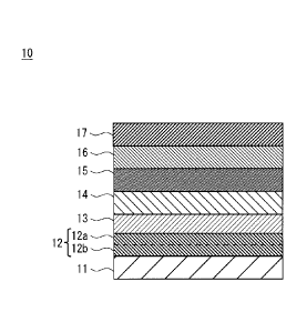
With reference to Fig. 1, a laminated structure of a secondary battery 10
according to the
present embodiment is described. Fig. 1 is a cross-sectional view
schematically showing a structure
of the secondary battery 10. The secondary battery 10 has a laminated
structure in which a first
electrode 11, a conductive layer 12, an n-type oxide semiconductor layer 13, a
charging layer 14, a
mixture layer 15, a p-type oxide semiconductor layer 16, and a second
electrode 17 are laminated in
this order.
[0022]
The first electrode 11 is formed of a conductive sheet or a conductive
substrate and serves
as a base material for providing the laminated structure. For example, a metal
foil sheet or the like
can be used as the first electrode 11. In this description, a steel use
stainless (SUS) sheet is used as
the first electrode 11. Alternatively, a metal foil sheet made of copper,
aluminium, or the like can be
used as the first electrode 11.
[0023]
In addition, by preparing a base material made of an insulating material, the
first electrode
11 can be formed on the based material. In the case of the first electrode 11
to be formed on the
base material, a metal material, such as chromium (Cr) or titanium (Ti), can
be used as the material
of the first electrode 11. An alloy film containing aluminium (Al), silver
(Ag), or the like can be
also used as the material of the first electrode 11. In the case of the first
electrode 11 to be formed
on the base material, the first electrode 11 can be formed similarly to the
second electrode 17 to be
CA 03032257 2019-01-28
described later.
[0024]
The conductive layer 12 can be formed of a metal material. The conductive
layer 12 has a
single layer structure consisting of a first metal film 12a, or a double layer
structure consisting of a
5 first metal film 12a and a second metal film 12b. Fig. 1 shows the double
layer structure consisting
of the first metal film 12a and the second metal film 12b. In the case of the
conductive layer 12
having the double layer structure, the second metal film 12b is in contact
with the first electrode 11,
and the first metal film 12a is in contact with the n-type oxide semiconductor
layer 13. In the case
of the conductive layer 12 having the single layer structure, the first metal
film 12a is in contact with
the n-type oxide semiconductor layer 13 and the first electrode 11.
[0025]
The material of the first metal film 12a preferably contains the same metallic
element as the
n-type oxide semiconductor layer 13. For example, when the n-type oxide
semiconductor layer 13
is titanium oxide (TiO2), the first metal film 12a is preferably titanium
(Ti). In addition, the
material of the first metal film 12a preferably contains an metallic element
having higher electric
conductivity than the electric conductivity of the metallic element contained
in the n-type oxide
semiconductor layer 13. For example, when the n-type oxide semiconductor layer
13 is titanium
oxide (TiO2), the first metal film 12a is preferably titanium (Ti), an alloy
containing titanium (Ti),
aluminium (Al), an alloy containing aluminium (Al), chromium (Cr), or nickel
(Ni).
[0026]
The second metal film 12b preferably contains a metallic element having higher
electric
conductivity than, for example, the electric conductivity of the metallic
element contained in the n-
type oxide semiconductor layer 13. For example, when the n-type oxide
semiconductor layer 13 is
titanium oxide (TiO2), the second metal film 12b is preferably aluminium (Al)
or tungsten (W).
[0027]
The conductive layer 12 may have, for example, a single layer structure
consisting of the
first metal film 12a being a titanium (Ti) film or a double layer structure
consisting of the first metal
film 12a being a titanium (Ti) film and the second metal film 12b being a
tungsten (W) film. The
thickness of the conductive layer 12 is 15 nm to 300 nm. The conductive layer
12 can be formed on
the first electrode 11 by sputtering or evaporation deposition.
[0028]
CA 03032257 2019701-28
6
The n-type oxide semiconductor layer 13 contains a second n-type oxide
semiconductor
material. As the material of the n-type oxide semiconductor layer 13, titanium
dioxide (TiO2), tin
oxide (Sn02), zinc oxide (Zn0), or the like can be used. The thickness of the
n-type oxide
semiconductor layer 13 is preferably 30 nm to 120 nm. For example, titanium
oxide having the
.. thickness of 60 to 120 nm can be used as the n-type oxide semiconductor
layer 13. For example, the
n-type oxide semiconductor layer 13 is formed on the first electrode 11 by
sputtering or evaporation
deposition.
[0029]
The charging layer 14 is formed of a mixture of an insulating material and an
n-type oxide
semiconductor material. For example, as the n-type oxide semiconductor
material (a first n-type
oxide semiconductor material) of the charging layer 14, n-type oxide
semiconductor fine particles
can be used. The n-type oxide semiconductor is turned into a layer having a
charging function
because the optical excitation structure is changed by irradiation with a
ultraviolet ray. The n-type
oxide semiconductor contains a mixture of an n-type oxide semiconductor
material and an insulating
material. As the insulating material, silicone resin is can be used. For
example, a silicon compound
(silicone), such as silicon oxide, having a main skeleton by a siloxane bond
is preferably used as the
insulating material.
[0030]
For example, the charging layer 14 is formed of silicon oxide and titanium
dioxide which is
used as the first n-type oxide semiconductor material. Besides, tin oxide
(Sn02) or zinc oxide
(ZnO) is suitable for the n-type oxide semiconductor material to be used for
the charging layer 14.
A material obtained by mixing two of titanium dioxide, tin oxide, and zinc
oxide or all of them can
be also used.
[0031]
A manufacturing process of the charging layer 14 is described below. First, a
coating liquid
is prepared by mixing, into a solvent, a mixture of a precursor of titanium
oxide, tin oxide, or zinc
oxide and silicone oil. A coating liquid is prepared by mixing fatty acid
titanium and silicone oil
into a solvent. Then, the coating liquids are applied on the n-type oxide
semiconductor layer 13 by a
spin coating method, a slit coating method, or the like. The coating film is
dried and calcined to
form the charging layer 14 on the n-type oxide semiconductor layer 13. Note
that, as an example of
the precursor, for example, titanium stearate which is a precursor of titanium
oxide can be used.
CA 03032257 2019-01-28
7
Titanium oxide, tin oxide, and zinc oxide are formed by decomposing aliphatic
acid salt which is a
precursor of metal oxide. The charging layer 14 after drying and calcining may
be irradiated with a
ultraviolet ray to be UV-cured.
[0032]
Note that, it is also possible to use, instead of a precursor, oxide
semiconductor fine
particles for titanium oxide, tin oxide, zinc oxide, or the like.
Nanoparticles of titanium oxide or
zinc oxide are mixed with silicone oil to obtain a liquid mixture. Then, the
liquid mixture is mixed
into a solvent to obtain a coating liquid. The coating liquid is applied on
the n-type oxide
semiconductor layer 13 by a spin coating method, a slit coating method, or the
like. The coating
film is dried, calcined, and UV-cured to form the charging layer 14.
[0033]
The mixture layer 15 is formed of a mixture of an insulating material and an n-
type oxide
semiconductor material. As the material of the insulating material, silicon
oxide can be used. For
example, when the insulating material is silicon oxide, the mixture layer 15
contains silicon dioxide
(SiO2). The insulating material of the mixture layer 15 may be the same
material as the insulating
material of the charging layer 14.
[0034]
As the material of the n-type oxide semiconductor material, tin oxide (SnO)
can be used. In
this case, the mixture layer 15 contains a mixture of silicon oxide and tin
oxide. In the mixture layer
15, the n-type oxide semiconductor material is added to silicon oxide, silicon
nitride, or silicone oil.
The n-type oxide semiconductor is diffused in silicon dioxide which is the
insulating material.
[0035]
The first n-type oxide semiconductor material contained in the charging layer
14 may be
the same as or different from the second n-type oxide semiconductor material
contained in the n-
type oxide semiconductor layer 13. For example, when the n-type oxide
semiconductor material
contained in the mixture layer 15 is tin oxide, the n-type oxide semiconductor
material contained in
the charging layer 14 may be tin oxide or another n-type oxide semiconductor
material except for tin
oxide.
[0036]
The thickness of the charging layer 14 is, for example, 200 nm to 1000 nm, and
the
thickness of the mixture layer 15 is 100 nm to 150 nm. The mixture layer 15
can be formed to have
CA 03032257 2019T01-28
8
the thickness of 50 nm to 250 nm. More preferably, the mixture layer 15 may be
formed to have the
thickness of 150 nm to 200 nm.
[0037]
The mixture layer 15 can be formed in a similar manufacturing process to that
for the
charging layer 14. First, a coating liquid is prepared by mixing, into a
solvent, a mixture of a
precursor of tin oxide and silicone oil. Then, the coating liquid is applied
on the charging layer 14
by a spin coating method, a slit coating method, or the like. The coating film
is dried and calcined
to form the mixture layer 15 on the charging layer 14. Tin oxide is formed by
decomposing
aliphatic acid which is a precursor of oxide semiconductor. The mixture layer
15 after drying and
calcining may be irradiated with a ultraviolet ray to be UV-cured.
[0038]
Note that, it is also possible to usc, instead of a precursor, oxide
semiconductor fine
particles for the oxide semiconductor material. Nanoparticles of tin oxide are
mixed with silicone
oil to obtain a liquid mixture. Then, the liquid mixture is mixed into a
solvent to obtain a coating
liquid. The coating liquid is applied on the charging layer 14 by a spin
coating method, a slit
coating method, or the like. The coating film is dried, calcined, and UV-cured
to form the mixture
layer 15.
[0039]
The p-type oxide semiconductor layer 16 contains a p-type oxide semiconductor
material.
As the material of the p-type oxide semiconductor layer 16, nickel oxide
(NiO), copper-aluminium
oxide (CuA102), or the like can be used. For example, the p-type oxide
semiconductor layer 16 is a
nickel oxide film having the thickness of 400 nm. The p-type oxide
semiconductor layer 16 is
formed on the mixture layer 15 by a film forming method such as sputtering or
evaporation
deposition.
[0040]
The second electrode 17 is only required to be formed of a conductive film. As
the material
of the second electrode 17, a metal material, such as chromium (Cr) or copper
(Cu), can be used.
Besides, a silver (Ag) alloy containing aluminium (Al) is also used. A forming
method of the
second electrode 22 includes vapor deposition such as spattering, ion plating,
electron beam
deposition, vacuum deposition or chemical deposition. In addition, the metal
electrode can be
formed by an electrolytic plating method or an electroless plating method. The
metal used for
CA 03032257 201901-28
9
plating is generally copper, a copper alloy, nickel, aluminium, silver, gold,
zinc, tin, or the like. For
example, the second electrode 17 is an Al film haying the thickness of 300 nm.
[0041]
<Effects of Invention>
In the secondary battery 10 according to the present embodiment, the mixture
layer 15 is
arranged between the charging layer 14 and the p-type oxide semiconductor
layer 16. The mixture
layer 15 is formed of a mixture of silicon oxide and a third n-type oxide
semiconductor material (a
conductive material). In comparison with a layer formed only of silicon oxide
(an insulating
material), the electric conductivity of the layer in the secondary battery
according to the present
embodiment can be adjusted by a conductive material, and it is possible to
secure a certain level of
electric conductivity although the mixture layer 15 is thickened. That is, it
is possible for the
mixture layer 15 to have a desired thickness in the secondary battery
according to the present
embodiment. Accordingly, it is possible to improve the performance of the
secondary battery 10.
[0042]
In addition, since it is possible for the mixture layer 15 to have a desired
thickness while a
certain level of conductivity is secured, it is unnecessary to form a layer to
be thin in order not to
obstruct the charge transfer unlike a layer formed only of silicon oxide (an
insulating material).
Thus, it is possible to prevent an uneven layer from being formed. That is, it
is possible to avoid
failures, such as localized dielectric breakdown in an uneven layer, in the
secondary battery
according to the present embodiment.
[0043]
Furtheiniore, the conductive layer 12 is arranged between the first electrode
11 and the n-
type oxide semiconductor layer 13 in the secondary battery 10 according to the
present embodiment.
The conductive layer 12 has a single layer structure including a titanium (Ti)
film as the first metal
film 12a or a double layer structure including a titanium (Ti) film as the
first metal film 12a and a
tungsten (W) film as the second metal film 12b.
<Single layer structure>
[0044]
When the conductive layer 12 has a single layer structure (the first metal
film 12a), the
conductive layer 12 containing a metal material (the metal material preferably
contains the same
metallic element as the metallic element contained in the n-type oxide
semiconductor layer 13 or a
CA 03032257 2019:01-28
metallic element having higher electric conductivity than that of the metallic
element contained in
the n-type oxide semiconductor layer 13) is arranged between the first
electrode 11 and the n-type
oxide semiconductor layer 13. For this reason, the current flows more easily
from the first electrode
11 to the n-type oxide semiconductor layer 13 in comparison with the case
where the conductive
5 layer 12 is not arranged. That is, by arranging the conductive layer 12,
the electric conductivity
from the first electrode 11 to the n-type oxide semiconductor layer 13 can be
adjusted. In addition,
by arranging the conductive layer 12, it is possible to improve the adhesion
between the first
electrode 11 and the n-type oxide semiconductor layer 13.
[0045]
10 When the surface of the first electrode 11 is oxidized without the
conductive layer 12, the
electric conductivity between the first electrode 11 and the charging layer 14
is lowered. By
arranging the conductive layer 12 on the first electrode 11, it is possible to
secure a certain level of
electric conductivity while oxidation of the surface of the first electrode 11
is reduced.
[0046]
When the n-type oxide semiconductor layer 13 is titanium oxide, the conductive
layer 12
(the first metal film 12a) preferably includes a titanium film which is the
same metallic element as
that of the n-type oxide semiconductor layer 13. This titanium film secures a
certain level of electric
conductivity and serves as an adhesion layer improving the adhesion between
the first electrode 11
and the n-type oxide semiconductor layer 13.
<Double structure layer>
[0047]
When the conductive layer 12 has a double layer structure (the first metal
film 12a and the
second metal film 12b), it is possible to suppress migration of the heavy
metal forming the first
electrode 11 to the n-type oxide semiconductor layer 13 and to improve the
adhesion between the
layer arranged on the second metal film 12b and the layer arranged under the
second metal film 12b,
in addition to the effects (conductivity and adhesion) when the conductive
layer 12 has the single
layer structure. The details of these effects are described with reference to
an example in which the
second metal film 12b is tungsten, and the second n-type oxide semiconductor
material contained in
the n-type oxide semiconductor layer 13 is titanium oxide (that is, the n-type
oxide semiconductor
layer 13 contains titanium as the metallic element).
[0048]
CA 03032257 2019-01-28
11
The electric resistivity of tungsten (W) is 5.29x10⁻⁸ S2m. The electric
resistivity of
titanium is 4.27x10⁻⁷ Qm. The electric resistivity is the reciprocal of the
electric conductivity. That
is, the metallic element contained in the second metal film 12b has higher
electric conductivity than
that of the metallic element contained in the second n-type oxide
semiconductor material. In other
words, by arranging the second metal film 12b, it is possible to secure
electric conductivity between
the first electrode 11 and the n-type oxide semiconductor layer 13. For
example, although it can be
possible to suppress migration by only arranging a layer having low electric
conductivity, the
resistance is too high to secure electric conductivity, and desired
performance of the battery cannot
be obtained. It is important to arrange a layer having higher electric
conductivity than that of the
metallic element contained in the second n-type oxide semiconductor material,
as the second metal
film according to the present embodiment.
[0049]
By forming the conductive layer 12 being a titanium film to have the thickness
of 15 nm,
the n-type oxide semiconductor layer 13 being a TiO film to have the thickness
of 60 nm, the
charging layer 14 to have the thickness of 1000 nm, the mixture layer 15 to
have the thickness of
150 nm, the p-type oxide semiconductor layer 16 being an NiO film to have the
thickness of 400
nm, and the second electrode 17 being an Al film to have the thickness of 300
nm, it is possible to
obtain high performance.
[0050]
Fig. 2 shows measurement results of energy density in the cases where the
conductive layer
12 is provided and is not provided. A measurement result A indicates the
measurement result of a
secondary battery in which the conductive layer 12 is a titanium single layer.
A measurement result
B indicates the measurement result of a secondary battery in which the
conductive layer 12 is not
provided and the first electrode 11 is in contact with the n-type oxide
semiconductor layer 13. Here,
the n-type oxide semiconductor material of the n-type oxide semiconductor
layer 13 is titanium
oxide. In addition, Fig. 2 shows the measurement result of each secondary
battery in which the
thickness of the charging layer 14 is 200 nm and the thicknesses of other
layers are changed.
[0051]
Specifically, the measurement result A in Fig. 2 indicates the measurement
result of the
secondary battery satisfying the following (condition 1) to (condition 4).
(Condition 1) The thickness of the n-type oxide semiconductor layer 13 is
changed in the
CA 03032257 2019:01-28
12
range of 65 to 120 nm.
(Condition 2) The thickness of the mixture layer 15 is changed in the range of
100 to 250
nm.
(Condition 3) A SUS foil is used as the first electrode 11 and its thickness
is changed in the
range of 5 to 10 um.
(Condition 4) The conductive layer 12 is provided in the secondary battery and
the
thickness of the conductive layer 12 is changed in the range of 15 to 120 nm.
[0052]
The measurement result B indicates the measurement result of the secondary
battery
satisfying the above (condition 1) to (condition 3). That is, the measurement
result B shows the
measurement result of the secondary battery in which the conductive layer 12
is not provided. In
addition, the measurement result of a secondary battery in which the
conductive layer 12 is a double
layer using tungsten as the first metal film 12a and titanium as the second
metal film 12b has been
substantially the same as the measurement result A of the secondary battery in
which the conductive
layer 12 is a titanium single layer.
[0053]
In each of the measurement results A and B in Fig. 2, the measurement values
of the energy
density in 15 samples are shown in a form of box plot. In the box plot form,
the upper 25% and the
lower 25% of the 15 samples are represented as boxes. The median of 15 samples
is indicated by a
thick horizontal line. The vertical axis indicates the energy density (Wh/l).
Comparing the
measurement result A in which the conductive layer 12 is provided with the
measurement result B in
which the conductive layer 12 is not provided, the measurement result A in
which the conductive
layer 12 is provided indicates that higher energy density is obtained.
[0054]
Note that, the second metal film 12b may contain a metallic element having
higher electric
conductivity than the electric conductivity of the metallic element contained
in the n-type oxide
semiconductor layer 13 and having a higher work function than the electric
conductivity of the
metallic element contained in the n-type oxide semiconductor layer 13. For
example, when then-
type oxide semiconductor layer 13 is titanium oxide (TiO2), the second metal
film 12b is preferably
tungsten (W). Note that, the work function of tungsten (W) is 4.52 eV. The
work function of
titanium is 4.14 eV.
A 4s,
13
[0055]
An example of an embodiment of the present invention has been described above,
and the
present invention includes appropriate modifications that do not harm its
purposes and advantages
and is not limited by the above embodiment.
Reference Signs List
[0056]
Secondary battery
11 First electrode
12 Conductive layer
10 12a First metal film
12b Second metal film
13 N-type oxide semiconductor layer
14 Charging layer
Mixture layer
15 16 P-type oxide semiconductor layer
17 Second electrode
CA 3032257 2020-02-25