Note: Descriptions are shown in the official language in which they were submitted.
CA 03033379 2019-02-07
WO 2018/039123 PCT/US2017/047800
ELECTRICAL CONNECTOR
CROSS-REFERENCE TO RELATED APPLICATION(S)
[0001] This application claims priority under 35 U.S.C. 119(e) to
Provisional Patent Application No.: 62/377,859, filed on August 22, 2016,
which is herein incorporated by reference.
TECHNICAL FIELD
[0002] The present disclosure relates to an electrical connector for
connecting electronic and/or electrical parts that may be misaligned.
BACKGROUND
[0003] In an electronic system it is necessary to establish electrical
connections between constituent parts of the system. Often, these parts are
relatively rigid and have fixed locations where the parts are to be connected
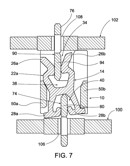
together. For example, the parts that are to be connected together may be
printed circuit boards (PCBs) and the connection locations may be plated
through-holes in the PCBs. While each PCB may be produced in compliance
with strict tolerances, the connection locations between the PCBs may
nonetheless become misaligned due to tolerance stacking or other reasons.
[0004] A misalignment between the connection locations of parts can
cause mating problems when the parts are connected together (or attempted
to be connected together). For example, as set forth above, one or both of the
parts may be a PCB with plated through-holes as connection points. In such a
situation, a connector is typically secured to the through-holes using
soldering
or press-fit connections. Such connections, which are rigid and relatively
fragile, can be physically damaged by errant forces that are produced when
the misaligned parts are brought together. Even if the parts are not damaged,
the electrical connections may not be as robust as they should be, due to the
misalignment.
[0005] Based on the foregoing, it would be desirable to provide an
electrical connector for electrically connecting parts, wherein the connector
accommodates misalignment between the parts.
CA 03033379 2019-02-07
WO 2018/039123 PCT/US2017/047800
SUMMARY
[0006] A connector is disclosed for connection to a substrate for
mounting
electronic devices. The substrate may have a plurality of holes formed
therein.
The connector includes a housing having opposing first and second end
openings. A coupling contact is pivotably disposed within the housing. The
coupling contact includes a pair of elements having opposing first and second
end portions, respectively. The elements are joined together, intermediate the
first and second end portions. The first end portions are separated by a first
space and the second end portions are separated by a second space. The
first space is aligned with the first end opening in the housing and the
second
space is aligned with the second end opening in the housing. The connector
also includes a mounting contact that is partially disposed within the
housing.
The mounting contact has a fastening structure joined to a bar section. The
fastening structure is adapted for insertion into one of the holes of the
substrate and the bar section is disposed in the second space of the coupling
contact.
[0007] In one aspect of the disclosure, the housing has a pair of
opposing
side walls, with one of the side walls having an opening. In addition, the
connector comprises a plurality of the contact plates, wherein the coupling
contacts are arranged side by side in a stack in the housing such that the
first
spaces are aligned to form a first receiving groove and the second spaces are
aligned to form a second receiving groove, which is aligned with the opening
in the side wall of the housing. The bar section of the mounting contact is
disposed in the second receiving groove.
BRIEF DESCRIPTION OF THE DRAWINGS
[0008] The features, aspects, and advantages of the present invention
will
become better understood with regard to the following description, appended
claims, and accompanying drawings where:
[0009] Fig. 1 shows a perspective view of a coupler of the disclosure;
[0010] Fig. 2 shows a partially disassembled perspective view of the
coupler
with a stack of contact plates removed from a housing;
[0011] Fig. 3 shows a plan view of one of the contact plates;
2
CA 03033379 2019-02-07
WO 2018/039123 PCT/US2017/047800
[0012] Fig. 4 shows a perspective view of a mounting contact for
connection
to the coupler;
[0013] Fig. 5 shows a perspective view of a connecting contact for
connection to a printed circuit board;
[0014] Fig. 6 shows a perspective view of a combination of the coupler,
mounting contact, connecting contact and a pair of printed circuit boards;
[0015] Fig. 7 shows a sectional view of the combination of Fig. 6;
[0016] Fig. 8 shows a perspective of a lead frame for connection to the
coupler;
[0017] Fig. 9 shows a perspective view of the lead frame connected to the
coupler disposed between a bus bar and a printed circuit board; and
[0018] Fig. 10 shows a perspective view of a pair of connectors.
DETAILED DESCRIPTION OF ILLUSTRATIVE EMBODIMENTS
[0019] It should be noted that in the detailed descriptions that follow,
identical components have the same reference numerals, regardless of
whether they are shown in different embodiments of the present disclosure. It
should also be noted that for purposes of clarity and conciseness, the
drawings may not necessarily be to scale and certain features of the
disclosure may be shown in somewhat schematic form.
[0020] Referring now to Figs. 1 and 2, there is shown a coupler 10
constructed in accordance with this disclosure. The coupler 10 is comprised of
a stack 12 of contact plates 14 disposed in a housing 16. Each of the contact
plates 14 is a unitary or monolithic structure and is electrically conductive,
being composed of a conductive metal, such as a tin plated copper alloy. As
best shown in Fig. 3, each contact plate 14 includes a pair of irregular-
shaped
elements or legs 18a,b. Each leg 18a,b includes an upper first portion 22a,b
with a dog leg configuration and a lower second portion 24a,b with a generally
L-shaped configuration. The first portion 22a,b includes a first end portion
26a,b that angles outwardly, relative to a longitudinal center axis L of the
contact plate 14, which extends between the legs 18a,b. The second portion
24a,b includes a second end portion 28a,b that extends laterally inward from
an outer heel and then, towards the longitudinal center axis L, bends upward.
The legs 18a,b are joined together by a cross bar 30, intermediate the first
3
CA 03033379 2019-02-07
WO 2018/039123 PCT/US2017/047800
and second end portions 26a,b, 28a,b. The cross bar 30 extends laterally
between the legs 18a,b and helps give the contact plate 14 a general H-
shape. The first end portions 26a,b define a first receiving space 34
therebetween, while the second end portions 28a,b define a second receiving
space 36 therebetween. Each of the first receiving spaces 34 has a wide
outer portion and a narrow inner portion, thereby giving the first receiving
space a general V-shape. Each of the second receiving spaces 36 is also V-
shaped; however, the first receiving space 34 is larger and its V-shape is
more pronounced than the second receiving space 36. The first receiving
space 34 adjoins a first inner space 38, while the second receiving space 34
adjoins a second inner space 40.
[0021] As shown, the contact plates 14 are disposed side-by-side, with
their planar surfaces adjoining each other, to form the stack 12. However, in
other embodiments, the contact plates 14 may be separated by spaces,
respectively. The contact plates 14 are aligned with each other such that the
first receiving spaces 34 form a first receiving groove 42 and the second
receiving spaces 36 form a second receiving groove 44. Similarly, the first
inner spaces 38 form a first inner passage 46 and the second inner spaces
form a second inner passage 48. The narrowest portion of the first receiving
groove 42, which directly adjoins the first inner passage 46 and is formed by
the narrow inner portions of the first receiving spaces 36, is referred to as
the
contact zone 49. The first and second receiving grooves 42, 44 and the first
and second inner passages 46, 48 extend in the stacking direction, which is
normal to the planar surfaces of the contact plates 14. The number of contact
plates 14 that are used is determined by the amount of electrical current the
coupler 10 is designed to handle, with the current carrying capacity of the
coupler 19 being increased by increasing the number of contact plates 14
used. Other factors that affect the current carrying capacity of the coupler
10
include the thickness of each contact plate 14, the type of plating used and
the composition of the underlying metal structure.
[0022] The housing 16 is generally cuboid and is composed of an
insulative material, such as plastic. The interior of the housing 16 is hollow
and is sized to receive the stack 12 of contact plates 14 in a press fit
operation, i.e., the interior is smaller in one or more dimensions than the
stack
4
CA 03033379 2019-02-07
WO 2018/039123 PCT/US2017/047800
12. The housing 16 includes opposing first side walls 54a,b, opposing second
side walls 50a,b and opposing first and second open ends 58, 60. The second
side walls 50a,b each have a rectangular major opening 62 disposed toward
the first open end 58 and a rectangular minor opening 64 disposed toward the
second open end 60. The first side walls 54a,b each have a rectangular major
slot 66 disposed toward the first open end 58 and a rectangular minor slot 68
disposed toward the second open end 60.
[0023] The contact plates 14 are secured within the housing 16 in a press-
fit operation in which the stack 12 as a whole is pressed into the housing 16
through the second open end 60. The resulting interference fit between the
stack 12 and the housing 16 secures the contact plates 14 within the housing
16, but permits pivoting motion of the contact plates 14, as will be discussed
more fully later.
[0024] The contact plates 14 are disposed within the housing 16 such that
the first receiving spaces 34 of the contact plates 14 are aligned with the
first
open end 58 of the housing 16 and the second receiving spaces 36 of the
contact plates 14 are aligned with the second open end 60 of the housing 16.
In addition, the first receiving groove 42 of the stack 12 is aligned with the
major slots 66 in the housing 16 and the second receiving groove 44 of the
stack 12 is aligned with the minor slots 68 in the housing 16.
[0025] For purposes of facilitating description, components of the
coupler
may be described with regard to X, Y, Z spatial coordinates, which are as
follows: the X-axis extends through the first side walls 54a,b of the coupler
10,
the Y-axis extends through the second side walls 50a,b of the coupler 10, and
the Z-axis extends through the first and second open ends 58, 60 of the
coupler 10.
[0026] The coupler 10 may be used in a variety of applications. In one
application, the coupler 10 may be used to connect together two bus bars,
with one bus bar being disposed in the first receiving groove 42 and the other
bus bar being disposed in the second receiving groove 44. The major slots 66
and the minor slots 68 in the housing 16 permit the coupler 10 to receive the
bus bars from different angles or directions. For example, both the first
receiving groove 42 and the second receiving groove 44 may receive a bus
bar that is oriented with its longitudinal axis parallel to the X-axis of the
5
CA 03033379 2019-02-07
WO 2018/039123 PCT/US2017/047800
coupler 10 or parallel to the Y-axis of the coupler 10. In this manner, the
two
bus bars connected by the coupler 10 can be arranged parallel to each other
in the direction of the X-axis or the Y-axis, or arranged perpendicular to
each
other.
[0027] In another application, the coupler 10 may be used to connect an
edge connector of a PCB to a bus bar, an electrical/electronic device, or an
edge connector of another PCB. The PCB edge connector may be disposed
in the second receiving groove 44, while a bus bar, bar-like portion of the
electrical/electronic device or an edge connector of the other PCB may be
disposed in the first receiving groove 42.
[0028] In still another application, a mounting contact may be used to
mount the coupler 10 to a substrate, such as a printed circuit board (PCB).
Different embodiments of the mounting contact may be used, depending on
the requirements of a particular application. One embodiment of the mounting
contact (designated by the reference numeral 74) is shown in Fig. 4. The
mounting contact 74 is a monolithic structure and is electrically conductive,
being composed of a conductive metal, such as a tin plated copper alloy. The
mounting contact 74 includes fastening structures 76 joined to a bar section
78. The bar section 78 is channel-shaped, having a center beam 80 joined
between opposing, outwardly-extending arms 82. A blade 84 is joined to an
upper portion of the beam 80 and has beveled surfaces that form an
elongated edge. The blade 84 does not span the entire length of the beam 80
between the arms 82, but is, instead, separated by spaces from the arms 82,
respectively. The blade 84 helps guide the beam 80 into the second receiving
groove 44 and the second inner passage 48 of the stack 12 of contact plates
14.
[0029] The fastening structures 76 are joined to a lower portion of the
beam 80 and extend outwardly therefrom, in a direction opposite the arms 82.
Each fastening structure 76 may have a press-fit construction. More
particularly, each fastening structure 76 may have an eye-of-the-needle
(EON) type of press-fit construction. With this type of construction, each
fastening structure 76 includes a center piercing 86 forming a pair of beams
88 that bow outwardly and are joined at an outer tip 90 and at an inner neck
92, which is joined to the beam 80. Each fastening structure 76 is adapted to
6
CA 03033379 2019-02-07
WO 2018/039123 PCT/US2017/047800
be press-fit into a hole in a substrate, such as the plated hole in the PCB
shown in Fig. 7. As the fastening structure 76 is being press-fit into the
hole,
the beams 80 initially deflect inward and then resiliently move outward to
provide a normal force against the PCB hole, thereby providing a reliable
physical and electrical connection.
[0030] The fastening structures used in the mounting contact 74 are not
limited to having an EON-type of press fit construction. Instead, fastening
structures having a different press-fit construction may be used, or the
fastening structures may simply be elongated pins that are soldered into the
holes of a PCB. In still another embodiment, the mounting contact 74 may
have a single fastening structure that includes a mount joined to the beam 80,
wherein the mount has a lower enlarged planar surface that may be soldered
to a metal plate of an insulated metal substrate, such as a metal core printed
circuit board.
[0031] The coupler 10 may be used with a connecting contact to connect
together two substrates, such as two PCBs, especially when higher currents
(30 amps or greater) are involved. Referring now to Fig. 5, such a connecting
contact 90 is shown. The connecting contact 90 has the same construction as
the mounting contact 74, except the connecting contact 90 has a bar section
92 that is different from the bar section 78. More specifically, the bar
section
92 only has a center beam 94, without any outwardly-extending arms. A blade
84 is joined to an upper portion of the beam 94. Fastening structures 76 are
joined to a lower portion of the beam 94 and extend outwardly therefrom. As
shown, each fastening structure 76 may have an EON type of press-fit
construction.
[0032] Referring now to Figs. 6 and 7, the coupler 10, the mounting
contact 74 and the connecting contact 90 are shown connecting together two
PCBs 100, 102, each of which has a plurality of plated through-holes that are
electrically conductive. The process of connecting together the PCBs 100,
102 begins with the coupler 10 and the mounting contact 74 being mounted to
the PCB 100, and the connecting contact 90 being mounted to the PCB 102.
The PCB 102 is then connected to the PCB 100 by inserting the connecting
contact 90 into the coupler 10.
[0033] The mounting contact 74 is secured to the coupler 10 by aligning
7
CA 03033379 2019-02-07
WO 2018/039123 PCT/US2017/047800
the bar section 78 of the mounting contact 74 with the second receiving
groove 44 of the coupler 10 and then applying a force to the mounting contact
74, while the coupler 10 is held still. The blade 84 guides the beam 80 into
the
second receiving groove 44 and the second inner passage 48 of the stack 12
of contact plates 14. The force is released when the beam 80 contacts inner
edges of the first side walls 54a,b defining upper ends of the minor slots 68.
At this point, the beam 80 extends through both the second inner passage 48
and the second receiving groove 44 and the arms 82 adjoin the first side walls
54a,b of the housing 16. In addition, the second end portions 28a,b of the
contact plates 14 press against the beam 84, thereby electrically connecting
the coupler 10 to the mounting contact 74. As will be discussed in more detail
below, the combination of the coupler 10 and the mounting contact 74 forms a
connector 105 that permits the PCB 100 to be connected to the PCB 102,
even though the PCBs may be misaligned.
[0034] Next, the connector 105 is secured to the PCB 100. The fastening
structures 76 are aligned with plated holes 106 in the PCB 100, respectively,
and then a force is applied to the connector 105, such as against the outer
ends of the arms 82. The fastening structures 76 deform as they enter the
holes 106 and then resiliently spring back to secure the fastening structures
76 within the holes 106. The connector 105 is now physically and electrically
connected to the PCB 100. It should be appreciated that with the housing 16
trapped between the arms 82 of the mounting contact, the coupler 10 is
provided with additional stability relative to the PCB 100 in the direction of
the
X-axis.
[0035] The connecting contact 90 is mounted to the PCB 102 by aligning
the fastening structures 76 with plated holes 108 in the PCB 102,
respectively,
and then applying a force, such as against outer end portions of the beam 94.
The fastening structures 76 deform as they enter the holes 108 and then
resiliently spring back to secure the fastening structures 76 within the holes
108, thereby physically and electrically connecting the connecting contact 90
to the PCB 102.
[0036] The PCB 102 is connected to the PCB 100 by inserting the beam
94 of the connecting contact 90 (secured the PCB 102) into the first receiving
groove 42 of the connector 105 (secured to the PCB 100). Since the PCB 102
8
CA 03033379 2019-02-07
WO 2018/039123 PCT/US2017/047800
and the PCB 100 are rigid bodies and they are to be connected with a low Z-
space therebetween, there may be some misalignment in the Y-direction
between the beam 94 and the first receiving groove 42. To better illustrate
the
operation of the connector 105, the beam 94 is shown as being offset to the
left (as viewed from Fig. 7) from the longitudinal center axes L of the
contact
plates 14. The connector 105, however, accommodates this misalignment. As
the beam 94 moves into the first receiving groove 42, the blade 84 contacts
sloping inner surfaces of the first end portions 26a of the contact plates 14,
which causes the contact plates 14 to pivot about the beam 80 (the X-axis) in
a counterclockwise direction (as viewed from Fig. 7) and guide the beam 94
into the contact zone 49. The major opening 62 in the second side wall 50a
permits this pivoting by receiving the first end portions 26a of the legs 18a
of
the contact plates 14. The pivotal movement of the contact plates 14 is shown
in Fig. 7 and is about eight and a quarter degrees. Even though the contact
plates 14 have pivoted out of their normal position, they still maintain a
good
physical and electrical connection with the beam 94, thereby establishing a
good physical and electrical connection between the PCB 102 and the PCB
100. As shown in Fig. 7, the beam 94 is pressed between inner surfaces of
the first end portions 26a,b of the contact plates 14 in the contact zone 49.
[0037] It should be appreciated that in addition to accommodating
misalignment in the Y-direction, the connector 105 also accommodates
misalignment in the X-direction and the Z-direction, as well as angular or
twist
misalignment in any of the three directions. The alignment of the the first
receiving groove 42 with the major slots 66 permits the beam 94 to be offset
in the X-direction vis-a-vis the first receiving groove 42 and still make a
good
physical and electrical connection with the contact plates 14. In the Z-
direction, the beam 94 does not need to extend into the first inner passage 46
to the full extent possible to make a good physical and electrical connection.
[0038] Another advantage provided by the connector 105 is that it
accommodates movement between parts that may occur after the parts have
been connected. For example, the parts may move relative to each other due
to environmental factors, such as temperature, vibration, impact or handling.
The connector 105 permits this relative movement, while still maintaining a
good electrical and physical connection between the parts.
9
CA 03033379 2019-02-07
WO 2018/039123 PCT/US2017/047800
[0039] In addition to being well suited to connect together two PCBs, the
connector 105 is well suited to connect together other rigid electronic
components. In particular, the attributes of the connector 105 make it
especially well suited for connecting a bus bar to a PCB to supply power
thereto. These attributes of the connector 105 include its small X-Y
footprint,
its ability to connect together misaligned rigid bodies and its ability to
accommodate larger currents. Indeed, the current capacity of the connector
105 is scalable by changing the number of contact plates 14 used and/or
changing the thickness, plating or structural composition of the contact
plates
14. Current capacities of 30 amps or more are achievable. When used to
connect a bus bar to a PCB, such as the PCB 100, an end or a portion of the
bus bar is disposed within the first receiving groove 42 and the first inner
passage 46 such that the enlarged planar surfaces of the bus bar engage the
inner surfaces of the first end portions 26a,b of the contact plates 14 in the
contact zone 49. Multiple connectors 105 may be used to mount a bus bar to
a PCB.
[0040] Depending on a particular connection between a PCB and bus bar,
the connector 105 may be modified to provide more stability against rotating
or tipping relative to the PCB as a result of the forces that may be applied
by
the bus bar. One such modification may be to replace the mounting contact
74 with a different type of mounting contact. For example, the mounting
contact 74 may be replaced with the mounting contact or lead frame 120,
which is shown in Fig. 8. The lead frame 120 is a monolithic, generally Z-
shaped structure and is electrically conductive, being composed of a
conductive metal, such as a tin plated copper alloy. The lead frame 120 has a
bar section 122 with fastening structures 76 extending outwardly therefrom.
The bar section 122 includes a center beam 124 having opposing ends joined
by bends 128 130 to arms 132, 134, respectively. The bends 128, 130 curve
in opposing directions to give the lead frame 120 its Z-shape. A blade 126 is
joined to an upper portion of the beam 124 and has beveled surfaces that
form an elongated edge. The arms extend upwardly beyond the blade 126.
Two of the fastening structures 76 are joined to lower portions of the arms
132, 134, respectively, and extend downwardly therefrom. A third (or center)
fastening structure 76 is joined to a lower portion of the beam 124 and
CA 03033379 2019-02-07
WO 2018/039123 PCT/US2017/047800
extends downwardly therefrom. A pair of supports 138 are also joined to the
lower portion of the beam 124 and extend downwardly therefrom. The
supports 138 bracket the center fastening structure 76.
[0041] It should be appreciated that the lead frame 120 may be modified
to
have a greater or lesser number of fastening structures 76 or to have a
different configuration. For example, instead of the bends 128, 130 curving in
opposing directions, the bends 128, 130 may curve in the same direction,
which would give the lead frame 120 a general U-shape. Still another example
would be having only one of the bends 128, 130 so that the lead frame 120
has a general L-shape.
[0042] Referring now to Fig. 9, the lead frame 120 is shown mounted to
the coupler 10 to form a connector 205, which will help connect a bus bar 140
to a PCB 142 to provide power thereto. Although not shown, multiple
connectors 205 may be used to mount the bus bar 140 to the PCB 142. The
lead frame 120 is mounted to the the coupler 10 by inserting the beam 124
into the second receiving groove 44 and the second inner passage 48 of the
coupler 10. With the beam 124 so positioned, the arms 132, 134 are disposed
against the first side walls 54a,b of the coupler 10, respectively. However,
the
first arm 132 is positioned against the first side wall 54b, toward the second
side wall 50a, while the second arm 134 is positioned against the first side
wall 54a, toward the second side wall 50b.
[0043] In the connector 205, the fastening structures 76 are not arranged
in the direction of the the X-axis, parallel to the second receiving groove
44,
as in the coupler 105. Instead, the fastening structures 76 are arranged
diagonal to the X-axis. Moreover, the fastening structures 76 are not all
positioned with their widths (beam to beam) extending in the direction of the
X-axis, as in the coupler 105. Instead, the outer fastening structures 76 are
positioned with their widths extending in the direction of the Y-axis, while
the
middle fastening structure 76 (joined to the beam 124) is positioned with its
width extending in the direction of the X-axis. When the connector 205 is
mounted to the PCB 142 by press-fitting the fastening structures 76 into the
plated holes 146 of the PCB 142, the foregoing arrangement of the fastening
structures 76 helps prevent the connector 205 from pivoting about the X-axis
and otherwise moving due to torsional and other forces applied by the bus bar
11
CA 03033379 2019-02-07
WO 2018/039123 PCT/US2017/047800
140. In this regard, it should be noted that when the connector 205 is mounted
to the PCB 142, the supports 138 of the lead frame 120 contact the surface of
the PCB 142 and help provide additional support for and stability to the
connector 205.
[0044] As shown in Fig. 9, the connector 205 may be used to mount a bus
bar to a PCB so that the enlarged planar surfaces and the short edges of the
bus bar are disposed perpendicular to the plane of the PCB, while the long
edges of the bus bar are parallel to the plane of the PCB. In order to mount a
bus bar to a PCB in orientations different than this, the connector 205 may be
modified. For example, if it is desired to mount a bus bar to a PCB so that
the
enlarged planar surfaces of the bus bar are parallel to the plane of the PCB,
the connector 205 may be modified to be mounted to the PCB so that both the
longitudinal axes L of the contact plates and the first receiving groove 42
are
parallel to the plane of the PCB, i.e., one of the second side walls 50a,b is
disposed adjacent to the PCB. The modifications utilized to accomplish this
change in mounting may include modifying the lead frame 120 to remove the
blade 126 and join an elongated tab or bar to the end of the arm 132, wherein
the bar extends rearwardly, with its planar surfaces disposed perpendicular to
the arm 132. The bar is inserted into the second receiving groove 44 of the
coupler 10 and the fastening structures 76 are press-fit into holes in the
PCB.
[0045] Other modifications may be made to the lead frame 120 to mount
the coupler 10 to a PCB in still other orientations. For example, the lead
frame
120 may be modified to replace the blade 126 with an elongated tab or bar,
which would be inserted into the second receiving groove 44 of the coupler
10. This modification of the lead frame 120 would permit the coupler 10 to be
mounted to a PCB such that the one of the first side walls 54a,b is disposed
adjacent to the PCB.
[0046] Referring now to Fig. 10, there is shown a connector assembly 150
for connecting together first and second PCBs to permit low current signals to
be transmitted therebetween. The connector assembly 150 includes a
connector 152 and a connector 154
[0047] The connector 152 includes a plurality of signal contacts 158
secured to a housing 156 composed of insulating material, such as plastic.
Each of the signal contacts 158 is a monolithic structure and is electrically
12
CA 03033379 2019-02-07
WO 2018/039123 PCT/US2017/047800
conductive, being composed of a conductive metal, such as a tin plated
copper alloy. Each signal contact 158 includes a fastening structure 76 joined
at its neck to a spade 160 with a beveled end. The fastening structures 76
and the the spades 160 extend outwardly from the housing 156 in opposing
directions. The fastening structures 76 are adapted to be press-fit into
plated
holes in a first PCB.
[0048] The connector 154 includes a housing 162 composed of insulating
material, such as plastic. The housing 162 has a plurality of pockets 166
arranged serially along its length. The pockets 166 have open top and bottom
ends and are separated from each other by interior walls. A series of side
slots 168 are formed in the front and rear sides of the housing 162, with each
pocket 166 having a pair of opposing slots 168. A single contact plate 14 is
press-fit into each pocket 166 such that the first portions 22a,b of the legs
18a,b are aligned with the opposing slots 168, respectively. With the contact
plate 14 so positioned, the first receiving space 34 of the contact plate 14
is
aligned with the open top end of the pocket 166 and the second receiving
space 36 of the contact plate 14 is aligned with the open bottom end of the
pocket 166. Each contact plate 14 is pivotably movable within its pocket 160.
[0049] A plurality of signal contacts 170 are mounted to the housing 162
and extend downwardly therefrom. Each of the signal contacts 170 is a
monolithic structure and is electrically conductive, being composed of a
conductive metal, such as a tin plated copper alloy. Each signal contact 170
includes a fastening structure 76 joined at its neck to a tab (not shown). The
fastening structures 76 are adapted to be press-fit into plated holes in a
second PCB. The tabs of the fastening structures 76 are inserted through the
open bottom ends into the pockets 166, respectively, so as to engage the
contact plates 14, respectively. More specifically, within each pocket 166,
the
tab of the fastening structure 76 is received within the second receiving
space
36 and the second inner space 40 of the contact plate 14, with the tab being
pressed between the inner surfaces of the second end portions 28a,b of the
contact plate 14.
[0050] It should be appreciated that the fastening structures 76 used in
the
connectors 152, 154 are not limited to having an EON-type of press fit
construction. Instead, fastening structures having a different press-fit
13
CA 03033379 2019-02-07
WO 2018/039123 PCT/US2017/047800
construction may be used, or the fastening structures may simply be
elongated pins that are soldered into the holes of a PCB.
[0051] After the connectors 152, 154 are mounted to the first and second
PCBs, the first and second PCBs are connected together by inserting the
spades 160 of the connector 152 (secured to the first PCB) into the first
receiving spaces 34 of the contact plates 14 of the connector 154 (secured to
the PCB 100). If the first and second PCBs are misaligned in the direction of
the front and rear sides of the housing 162, the spades 160 will contact the
sloping inner surfaces of the first end portions 26a (or the first end
portions
26b) of the contact plates 14, thereby pivoting the contact plates 14 about
the
tabs of the signal contacts 170, respectively. The side slots 168 in the
housing
162 permit this pivoting.
[0052] It is to be understood that the description of the foregoing
exemplary
embodiment(s) is (are) intended to be only illustrative, rather than
exhaustive.
Those of ordinary skill will be able to make certain additions, deletions,
and/or
modifications to the embodiment(s) of the disclosed subject matter without
departing from the spirit of the disclosure or its scope.
14