Note: Descriptions are shown in the official language in which they were submitted.
CA 03033657 2019-02-11
WO 2018/031244 PCT/US2017/044184
IMPROVED ELECTRONIC DETONATOR, ELECTRONIC IGNITION MODULE (EIM)
AND FIRING CIRCUIT FOR ENHANCED BLASTING SAFETY
REFERENCE TO RELATED APPLICATION
[001] The present application claims priority to and the benefit of U.S.
Provisional Patent
Application No. 62/373,715, filed August 11, 2016 and entitled ELECTRONIC
DETONATOR
WITH ENHANCED SAFETY AT LOGGER LEVEL, the entirety of which is hereby
incorporated by reference.
BACKGROUND AND INCORPORATION BY REFERENCE
[002] Blasting is used in the recovery of mineral resources, including in
surface mining and
quarrying for rock fragmentation and displacement of the broken rock. In
blasting operations,
detonators and explosives are buried in the ground, for example, in holes
(e.g., bore holes) drilled
into rock formations, etc., and the detonators are wired for external access
to blasting machines
that provide electrical signaling to initiate detonation of explosives.
Electronic detonators have
been developed which implement programmable delay times such that an array of
detonators can
be actuated in a controlled sequence. Electronic detonators are programmed
using a logger, and
later actuated or ignited using a blasting machine. The logger and the
blasting machine to
provide different voltages to a connected detonator in order to guard against
inadvertent ignition
during logging or programming operations. The electronic detonator typically
includes a storage
capacitor to store power to operate the internal detonator circuitry for
reading and writing
operations during programming by a logger. In addition, the detonator includes
a firing capacitor
that can be charged while the detonator is connected to a blasting machine, in
order to selectively
provide energy to an ignition element in response to a firing signal from the
blasting machine.
Ideally, the firing capacitor is not charged by a connected logger, but
instead is charged only
once a higher voltage blasting machine is connected to the detonator. In
particular, each
detonator in an electronic detonator blasting system may be queried
electrically by a logger or
programming unit, which contains voltage and current power sources. Such power
sources
should be insufficient to cause firing in the logger mode, or contain enough
number of failure
modes resulting in low likelihood of firing the electronic detonator during
the logging or
1
CA 03033657 2019-02-11
WO 2018/031244 PCT/US2017/044184
programming phase in the field. Optical means (e.g., bar code scanners, etc.)
can instead be used
for logging without any electrical signal exchange between the logger and
electronic detonator,
but it is more efficient to make electrical contact to also confirm that
electrical communication
exists and is reliable. Notably if there is a cut legwire, or a faulty
electronic circuit inside the
electronic detonator, such electrical contact, communication and/or
diagnostics can alert the
blaster of any potential issues, which would not otherwise be revealed using
only optical logging.
Further developments would therefore be beneficial to alleviate the
probability of inadvertent
firing during electrical communications to enhance the level of safety for
electronic detonators
connected to loggers over the boreholes containing explosives. The following
documents are
incorporated by reference in their entireties: US Pat 9,243,877; US Pat
5,309,841; US Pat
7,301,750; US Pat 4,393,779; European patents EP 1831636 and EP 2 352 964 and
Published
International Application WO 2011/014891.
SUMMARY
[003] Various aspects of the present disclosure are now summarized to
facilitate a basic
understanding of the disclosure, wherein this summary is not an extensive
overview of the
disclosure, and is intended neither to identify certain elements of the
disclosure, nor to delineate
the scope thereof. Instead, the primary purpose of this summary is to present
some concepts of
the disclosure in a simplified form prior to the more detailed description
that is presented
hereinafter. Disclosed examples include firing control electronic circuits,
such as electronic
ignition modules (ElMs), electronic detonators and firing circuits for
blasting applications, in
which one or more diodes is/are is coupled between a firing capacitor and
charging voltage
source in a circuit with a detonator ignition element to block voltage below a
certain desired
level so that the firing capacitor is not charged to enhance safety in the
logger mode.
BRIEF DESCRIPTION OF THE DRAWINGS
[004] The following description and drawings set forth certain illustrative
implementations of
the disclosure in detail, which are indicative of several exemplary ways in
which the various
principles of the disclosure may be carried out. The illustrated examples,
however, are not
exhaustive of the many possible embodiments of the disclosure. Other objects,
advantages and
2
CA 03033657 2019-02-11
WO 2018/031244 PCT/US2017/044184
novel features of the disclosure will be set forth in the following detailed
description of the
disclosure when considered in conjunction with the drawings, in which:
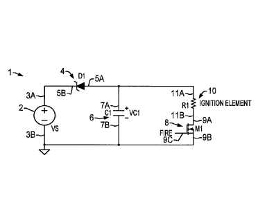
[005] Fig. 1 is a schematic diagram illustrating an example firing circuit for
an electronic
detonator including a Zener diode disposed between a charging voltage source
and a firing
capacitor.
[006] FIG. 2 is a graph of firing capacitor voltage as a function of charging
source bus voltage.
[007] FIG. 3 is a sectional view of an electronic detonator including an
electronic ignition
module (EIIVI) with the firing circuit of FIG. 1.
DETAILED DESCRIPTION
[008] Referring now to the figures, several embodiments or implementations of
the present
disclosure are hereinafter described in conjunction with the drawings, wherein
like reference
numerals are used to refer to like elements throughout, and wherein the
various features and plots
are not necessarily drawn to scale. The terms "couple" or "couples" or
"coupled" are intended to
include indirect or direct electrical or mechanical connection or combinations
thereof. For
example, if a first device couples to or is coupled with a second device, that
connection may be
through a direct electrical connection, or through an indirect electrical
connection via one or
more intervening devices and connections.
[009] Referring initially to FIGs. 1 and 3, disclosed examples include firing
control electronic
circuits, referred to herein as electronic ignition modules EINIs 23,
electronic detonators 20 and
firing circuits 1 for blasting applications, in which a Zener diode 4 (D1 in
FIG. 1) is coupled
between a firing capacitor 6 and charging voltage source 2 in a circuit with a
detonator ignition
element 10 to block voltage below a certain desired level so that the firing
capacitor 6 is not
charged to enhance safety. In other implementations, a general diode can be
coupled between the
firing capacitor 6 and the charging voltage source 2. The polarity is reversed
for a normal diode
(e.g., anode to charging source) than for a Zener diode 4 (e.g., anode to
ignition element as
shown in FIG. 1). In other examples, multiple diodes can be coupled between
the firing capacitor
6 and the charging voltage source 2, including general diodes, Zener diodes or
combinations
thereof. The EINI 23 in one example includes a fusehead or bridgewire or other
suitable ignition
element 10 (shown as R1 in FIG. 1), for example, compliant with appropriate
Bruceton all-fire
3
CA 03033657 2019-02-11
WO 2018/031244 PCT/US2017/044184
and no-fire specifications. The Zener diode 4 is connected in series with one
or more firing
capacitors 6 (Cl), herein referred to as a firing capacitor Cl whether a
single capacitor
component or multiple capacitors connected in series and/or parallel with one
another or
combinations thereof.
[0010] The ElM 23 in certain embodiments includes a tantalum capacitor 6,
although other
capacitor types can be used such as electrolytic, ceramic, etc., in series
with the Zener diode 4.
The improved ELVI examples 23 can advantageously employ small surface mount
tantalum
capacitors 6 instead of larger radial aluminum electrolytic capacitors to
facilitate circuit board
manufacturing and final assembly of an electronic detonator assembly 20 (FIG.
3). Moreover, the
novel Zener-based firing circuit 1 enhances blasting site safety and
reliability by fully or at least
partially blocking the firing capacitor 6 from voltage of a connected logger
(not shown). For
example, certain implementations use a low leakage 8.2 V Zener diode 4
connected in series
with the firing capacitor 6 to block any voltage beyond 8.2 V, therefore
practically cutting off a
typical logger bus voltage of 7.5 V from ever reaching the firing capacitor 6
and bridgewire
network 10. Moreover, the series connected Zener 4 attenuates the voltage
imposed on the firing
capacitor 6, thereby allowing the use of compact, lower voltage tantalum (Ta)
capacitor(s) 6 with
an acceptable voltage rating, where tantalum capacitors 6 provide better
reliability and
performance during firing discharge compared with larger electrolytic types.
[0011] Certain disclosed examples may employ a low leakage Zener 4 to
advantageously obtain
a sharper more controlled blocking Zener knee voltage. In operation in a
blasting application,
individual detonators 20 are queried electrically by a logger or programming
unit (not shown),
which includes voltage and current power sources. Such power sources are
ideally insufficient to
cause firing in the logger mode.
[0012] FIG. 1 shows a firing circuit example 1 in which the Zener 4 is
connected between the
charging voltage source 2 and the firing capacitor 6 but before the fusehead
or ignition element
10, and FIG. 3 shows an electronic detonator 20 with an EIM 23 including the
firing circuit 1 of
FIG. 1. The firing circuit 1 includes the charging source 2 including first
and second (e.g.,
positive and negative) charging source terminals 3A and 3B, where the charging
source 2 is
configured in one example to selectively provide a charging voltage signal VS
between the first
and second charging source terminals 3A, 3B. In certain examples, the charging
source 2
4
CA 03033657 2019-02-11
WO 2018/031244 PCT/US2017/044184
provides the charging voltage signal VS using power obtained from leg wires 19
from a
connected blasting machine or logger device (FIG. 3). In certain examples,
moreover, the
charging source 2 is configured to selectively provide the charging voltage
signal VS including a
positive voltage at the first charging source terminal 3A relative to the
second charging source
terminal 3B. The firing circuit 1 includes an ignition element 10 with first
and second electrical
terminals 11A and 11B, respectively. As seen in FIG. 3, the ignition element
10 is operatively
associated with a base charge 36 of the electronic detonator assembly 20 to
selectively ignite the
base charge 36 in response to conduction of electrical current through the
ignition element 10.
[0013] The circuit 1 in FIG. 1 also includes the Zener diode D1 (4) with an
anode 5A connected
to the first electrical terminal 11A of the ignition element 10, and a cathode
5B connected to the
first charging source terminal 3A of the charging source 2. The Zener diode 4
in one
embodiment has a Zener voltage (Vz) of approximately 8.2 V for use with
loggers that provide a
voltage of about 7.5 V on the detonator leg wires 19 (FIG. 3). In certain
examples, the Zener
diode 4 is a low leakage Zener diode. The firing capacitor Cl (6) includes a
first capacitor
terminal 7A connected to the first electrical terminal 11A of the ignition
element 10, and a
second capacitor terminal 7B connected to the second charging source terminal
3B of the
charging source 2. The firing capacitor 6 in certain examples includes at
least one tantalum
capacitor. The circuit 1 also includes a switching device 8 (e.g., MOSFET M1)
connected
between the second electrical terminal 11B of the ignition element 10 and the
second charging
source terminal 3B of the charging source 2. The switch 8 can be below or on
top of the ignition
element next to the firing capacitor 6. The switch 8 can be contained inside
an ASIC or a
separate component, e.g. MOSFE,T, BJT, MESPET, bipolar transistor, or other
suitable electrical
switch including a control terminal to receive a control signal FIRE to
selectively connect the
second electrical teiminal 11B of the ignition element 10 to the second
charging source terminal
3B of the charging source 2 to allow current to flow through the ignition
element 10 ignite the
base charge 36. The host EIM 23 in FIG. 3 includes a control circuit 30, such
as an ASIC, to
selectively provide the control signal FIRE to operate the switching device 8,
and the control
circuit 30 in certain examples is programmable to provide the control signal
FIRE at the
programmed delay time after the EIM 23 receives an input FIRE signal from a
connected
blasting machine (not shown) via leg wires 19 in FIG. 3.
CA 03033657 2019-02-11
WO 2018/031244 PCT/US2017/044184
[0014] FIG. 3 shows an electronic detonator 20, including a housing 29 with an
interior, a base
charge 36 disposed within the interior of the housing 29, where the ignition
element 10 is
operatively associated with the base charge 36 to selectively ignite the base
charge 36 in
response to conduction of electrical current through the ignition element 10.
The detonator 20
also includes a pair of wires 19 (leg wires) coupled with the EIM 23 to allow
delivery of an input
signal from a connected blasting machine (not shown) to the electronic
detonator 20. As shown
in FIG. 3, the detonator 20 is an electronic detonator with a programmable
delay time, including
an EIM 23 implementing the firing circuit 1 of FIG. 1, a shell housing or
enclosure 29, the base
charge 36 (preferably comprising a primary charge and base charge), the leg
wires 19, and an
end plug 34 that may be crimped in the open end of the shell 29. The EIM 23 is
preferably
programmable and includes an ignition element or fusehead 10 and a circuit
board with various
electronic components implementing the EIM 23 and the firing circuit 1.
[0015] The ignition element 10 in one example is a hermetically sealed device
that includes a
glass-to-metal seal and a bridgewire 27 designed to reliably ignite a base
charge contained within
the ignition element 10 upon the passage through the bridgewire 27 of
electricity via pins 11A
and 11B at a predetermined "all-fire" voltage level. The ignition element 10
can also consist of a
fusehead, for example. The EIM 23 (including its electronics and part or all
of its ignition
element 10) may be insert-molded into an encapsulation 31 to form a single
assembly with
terminals for attachment of the leg wires 19. U.S. patent application
Publication
2003/0221575A1, published December 4, 2003 and U.S. patent application
Publication
2003/0221576A1, published December 4, 2003, are hereby incorporated by
reference for their
applicable teachings of the construction of such detonators 20 beyond the
description that is set
forth herein. The EIM 23 can be manufactured and handled in standalone form,
for later
incorporation by a user into the user's own custom detonator assembly
(including a shell 29 and
base charge 36). The encapsulation 31 can be alternatively replaced by other
packaging methods
or materials such as heat shrink, epoxy or conformal coating.
[0016] The circuit board of the EIM 23 includes a control circuit, such as a
microcontroller or
programmable logic device or an application-specific integrated circuit chip
(ASIC) 30 to
selectively provide the FIRE control signal to operate the switch 8, as well
as a filtering
capacitor, a storage capacitor 25 to hold an electrical charge and power the
EIM 23 when the
6
CA 03033657 2019-02-11
WO 2018/031244 PCT/US2017/044184
detonator 20 is responding back to a master device (not shown), the firing
capacitor 6 (e.g., 47 to
374 liF) to hold an energy reserve that is used to selectively fire the
detonator 20 when the switch
8 is closed, additional electronic components, and contact pads 22 for
connection to the leg wires
19 and the ignition element 10. A shell ground connector 32 protruding from
the EIM 23 for
contact with the shell 29 is connected to, e.g., a metal can pin on the
circuit board within the EIIVI
23 (further connected to, e.g., an integrated silicon controlled resistor or a
diode) that can provide
protection against electrostatic discharge and radio frequency and
electromagnetic radiation that
could otherwise cause damage and/or malfunctioning. The ASIC 30 in one example
is a mixed
signal chip with inputs to the leg wires 19 and for connection to the shell
29, a connection to the
firing capacitor 6 and bridgewire 27 of the ignition element 10.
[0017] The charging source 2 provides the supply voltage VS inside the
electronic detonator 20,
having voltage from 12 V to as high as 42 V in operation. The firing capacitor
6 stores the
electrical charge in the armed state, ready to discharge into the ignition
element 10 at the
designated programmed delay time when the control circuit closes the switch 8.
The ignition
element (R1) is the active bridgewire which ignites upon sufficient energy
from capacitive
discharge from the firing capacitor 6. The switch 8 turns on according to the
FIRE control signal
from the control circuit (ASIC) 30 to allow the passage of electrical charge
energy stored in the
firing capacitor 6 at the appropriate delay time.
[0018] The Zener diode 4 (D1) is connected between the charging source VS and
the firing
capacitor Cl. The cathode of the Zener diode is connected to the same node at
the positive of the
charging source, VS. The anode of the Zener diode 4 is connected to the same
node as the firing
capacitor Cl. In this configuration, a voltage drop exists between charging
source 2 and the
firing capacitor 6, by which the ignition element 10 sees the diminished
voltage from the firing
capacitor. For example, using an 8.2 V Zener 6, the voltage difference is the
value of the voltage
drop across the Zener 4 thus alleviating the net voltage seen by the firing
capacitor 6. For
example, for charging source VS of 20 V, the voltage on the firing capacitor 6
is 20 ¨ 8.2 = 11.8
V. Additionally if the bus voltage VS is 8.2 V or lower, there is no voltage
at all on the firing
capacitor 6. Therefore, if a logger operating at 7.5 V or 8 V is connected to
the legwires 19, if a
voltage is inadvertently developed on the charging source 2, the net voltage
is still zero on the
7
CA 03033657 2019-02-11
WO 2018/031244 PCT/US2017/044184
firing capacitor 6. Thus, the EIM 23 adds a further level of safety through
the rejection of
elevated voltage beyond a certain point, especially at typical logger
operating voltage levels.
[0019] FIG. 2 is a graph 12 showing Firing Cap Voltage vs. Bus Voltage curve
14 with the
Zener diode 4 in the circuit 1, and a comparison curve 16 where no Zener 4 is
used. There is a
slope on the curve 14 of the effective voltage on the firing cap as a function
of the input bus
voltage VS, and the voltage on the capacitor both curves 14 and 16 start
saturating at bus voltage
above 28 V. In the example EIM 23 with the Zener diode 4, there is no voltage
at all on the firing
capacitor 6 at bus voltages of 11.0 V or below (curve 14), and the typical
logger bus voltage is
nominally 7.5 V. In one failure mode of ASIC breakdown and in an unlikely
scenario of the
firing capacitor 6 charging directly from bus logger voltage (curve 16), the
Zener diode 4 keeps
the voltage essentially at zero volts (curve 14).
[0020] There are a variety of possible variations such as different types or
ranges of materials,
dimensions, configurations, modifications, parts, options, etc. that might
reasonably achieve
roughly the same goals. Certain advantages are facilitated by the disclosed
examples, including
the ability to use tantalum capacitors 6 for easy assembly into EIM PCBs via
pick and place of
surface mount components 6 without requiring manual soldering or placement as
with larger
electrolytic capacitor types. Additionally, the tantalum capacitors 6 are more
robust
mechanically, whereas aluminum electrolytic capacitors are more prone to
dynamic pressure
crushing. The new disclosed examples alleviate potential misfires resulting
from damaged firing
capacitors. The use of the Zener diode 4 blocks voltage of a predetermined
value (e.g., 8.2 V)
from firing capacitor, and provides a safer detonator 20 at logger mode in
case of bus voltage
inadvertently applied across firing capacitor 6, and allows the use of smaller
and lower voltage
rated capacitors, thereby saving space and cost. Moreover, if the Zener were
instead placed
between the firing capacitor 6 and the fusehead/ignition element 10, it would
need to be high
wattage to conduct the high current safely, and due to finite resistance in
the Zener, there will be
lost power and energy across this Zener in delivering the energy to the
ignition element. In
contrast, in the disclosed example, when then Zener 4 is placed before the
firing capacitor 6 there
is a direct path form the firing capacitor 6 to the ignition element 10 thus
ensuring more efficient
energy transfer from the firing capacitor 6 to the ignition element 10.
8
CA 03033657 2019-02-11
WO 2018/031244 PCT/US2017/044184
[0021] The example embodiments have been described with reference to the
preferred
embodiments. Modifications and alterations will occur to others upon reading
and understanding
the preceding detailed description. It is intended that the exemplary
embodiment be construed as
including all such modifications and alterations insofar as they come within
the scope of the
appended claims or the equivalents thereof. The above examples are merely
illustrative of
several possible embodiments of various aspects of the present disclosure,
wherein equivalent
alterations and/or modifications will occur to others skilled in the art upon
reading and
understanding this specification and the annexed drawings. In particular
regard to the various
functions performed by the above described components (assemblies, devices,
systems, circuits,
and the like), the terms (including a reference to a "means") used to describe
such components
are intended to correspond, unless otherwise indicated, to any component, such
as hardware,
processor-executed software and/or firmware, or combinations thereof, which
performs the
specified function of the described component (i.e., that is functionally
equivalent), even though
not structurally equivalent to the disclosed structure which performs the
function in the
illustrated implementations of the disclosure. In addition, although a
particular feature of the
disclosure may have been disclosed with respect to only one of several
implementations, such
feature may be combined with one or more other features of the other
implementations as may be
desired and advantageous for any given or particular application. Also, to the
extent that the
terms "including", "includes", "having", "has", "with", or variants thereof
are used in the detailed
description and/or in the claims, such terms are intended to be inclusive in a
manner similar to
the term "comprising."
9