Note: Descriptions are shown in the official language in which they were submitted.
CA 03034236 2019-02-15
Optical Modulator
Technical Field
[0001] The present invention relates to a charge-
accumulation-type optical modulator using a NOS structure
consisting of compound semiconductors.
Background Art
[0002] Technology of integrating compound semiconductor
elements on a silicon-on-insulator (SOI) substrate
utilized as a communication optical device is attracting
more attention. Particularly, technology of integrating a
laser and an optical modulator is important as to
dramatically increase integration density of communication
devices and to reduce the cost. For an optical modulator
that needs higher speed and efficiency, a charge-
accumulation-type optical modulator with a NOS structure
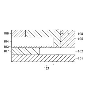
including an n-type InP layer and a p-type Si layer with
little optical loss has potential to achieve those needs
(see non-patent literature 1).
[0003] As shown in Fig. 4, this optical modulator is
formed from a p-type silicon layer 402 formed on a buried
insulating layer 401, an insulating layer 403 formed on
the p-type silicon layer 402, and an n-type InP layer 404
formed on the insulating layer 403. A p-electrode 405 is
connected to the p-type silicon layer 402, and an n-
1
CA 03034236 2019-02-15
electrode 406 is connected to the n-type InP layer 404.
The buried insulating layer 401 functions as a clad. The
p-type silicon layer 402 is formed by patterning an SOI
layer 411 on the buried insulating layer 401. An air
groove 412 is formed in a side portion of the p-type
silicon layer 402 on the formation side of the n-electrode
406 with the SOI layer 411. The upper surface of the n-
type InP layer 404, which is not covered with the n-
electrode 406, is open to a space.
[0004] Part of the p-type silicon layer 402 and part of
the n-type InP layer 404 are arranged so as to overlap
each other in a planar view, and form an optical waveguide
portion where light to be modulated is guided. In this
optical waveguide portion, the insulating layer 403 is
sandwiched between the p-type silicon layer 402 and the n-
type InP layer 404 in a stacking direction. Light to be
modulated is confined in a light confinement portion
including clad regions consisting of buried insulating
layer 401, the air groove 412, an upper space, and the
like, thereby forming a waveguide mode 421.
[0005] In this optical modulator, by modulating the
concentration of majority carriers accumulated at the
interfaces between the p-type silicon layer 402 and the n-
type InP layer 404 with the insulating layer 403 in the
optical waveguide portion, the refractive indices of the
2
CA 03034236 2019-02-15
p-type silicon layer 402 and the n-type InP layer 404 in
the optical waveguide portion are modulated. In this
structure, an improvement in modulation efficiency is
expected to be about two to three times greater, as
compared to a case in which Si is used for an n-type
layer.
Related Art Literature
Non-Patent Literature
[0006] Non-Patent Literature 1: D. Liang et al., "A
Tunable Hybrid III-V-on-Si MOS Microring Resonator with
Negligible Tuning Power Consumption", Optical Fiber
Communication Conference 2016, ThlK.4, 2016.
Disclosure of Invention
Problem to be Solved by the Invention
[0007] However, the above-described technology has a
problem that it is not easy to achieve further improvement
in modulation efficiency. To improve modulation
efficiency, it is important to increase a carrier-induced
refractive index change (carrier plasma effect). In
addition, to improve modulation efficiency, it is
important to further increase the action (influence) of
generated carriers on guided light. In theory, the
carrier-induced refractive index change can be further
increased by reducing the effective mass of a compound
semiconductor and increasing the band filling effect.
3
CA 03034236 2019-02-15
Furthermore, it is possible that the greater action of the
carriers on the guided light is achieved by increasing a
light confinement coefficient.
[0008] In fact, however, InP that is used in the
conventional technology and forming the InP layer is a
stoichiometrically stable composition, and has a uniquely
decided crystal structure. Therefore, the material
physical properties such as the effective mass and
refractive index cannot be adjusted. According to the
above-described two factors, it is extremely difficult to
improve modulation efficiency.
[0009] The present invention has been made in
consideration of the above problems, and has as its object
to further improve the modulation efficiency of a charge-
accumulation-type optical modulator with a MOS structure.
Means of Solution to the Problem
[0010] According to the present invention, there is
provided an optical modulator including a p-type first
semiconductor layer made of one of silicon and silicon-
germanium formed on a clad layer, an insulating layer
formed on the first semiconductor layer, an n-type second
semiconductor layer formed from a III-V compound
semiconductor made of at least three materials formed on
the insulating layer, a first electrode connected to the
first semiconductor layer, and a second electrode
4
CA 03034236 2019-02-15
connected to the second semiconductor layer, wherein part
of the first semiconductor layer and part of the second
semiconductor layer are arranged so as to overlap each
other via the insulating layer in a planar view, and form
an optical waveguide portion where light to be modulated
is guided in a direction parallel to a plane of the clad
layer, and the light waveguide portion satisfies a single
mode condition.
[0011] In the optical modulator, the first electrode is
formed on a region of the first semiconductor layer where
the optical waveguide portion is not being formed.
[0012] In the optical modulator, the second
semiconductor layer is formed from stacked multiple
compound semiconductor layers, and among the plurality of
compound semiconductor layers, the compound semiconductor
layer closer to the insulating layer has a smaller band
gap energy.
[0013] In the optical modulator, the first
semiconductor layer is formed from stacked multiple
semiconductor layers, and among the plurality of
semiconductor layers, the semiconductor layer closer to
the insulating layer has a smaller bandgap energy.
Effect of the Invention
[0014] As described above, according to the present
invention, since an n-type second semiconductor layer is
CA 03034236 2019-02-15
formed by a III-V compound semiconductor made of three or
more materials, it is possible to obtain an excellent
effect capable of further improving the modulation
efficiency of a charge-accumulation-type optical modulator
with a MOS structure.
Brief Description of Drawings
[0015] Fig. 1 is a sectional view showing the
arrangement of an optical modulator according to the first
embodiment of the present invention;
Fig. 2 is a plan view showing the partial
arrangement of the optical modulator according to the
first embodiment of the present invention;
Fig. 3 is a sectional view showing the
arrangement of an optical modulator according to the
second embodiment of the present invention; and
Fig. 4 is a sectional view showing the
arrangement of a conventional charge-accumulation-type
optical modulator with a MOS structure.
Best Mode for Carrying Out the Invention
[0016] Embodiments of the present invention will be
described below with reference to the accompanying
drawings.
[0017] [First Embodiment]
The first embodiment of the present invention
6
CA 03034236 2019-02-15
will be described with reference to Figs. 1 and 2. Fig. 1
is a sectional view showing the arrangement of an optical
modulator according to the first embodiment of the present
invention. Fig. 2 is a plan view showing the partial
arrangement of the optical modulator according to the
first embodiment of the present invention.
[0018] The optical modulator includes a p-type first
semiconductor layer 102 formed on a clad layer 101, an
insulating layer 103 formed on the p-type first
semiconductor layer 102, and an n-type second
semiconductor layer 104 formed on the insulating layer
103. The first semiconductor layer 102 is made of silicon
or silicon-germanium. The second semiconductor layer 104
is formed from a compound semiconductor made of three or
more materials. The second semiconductor layer 104 is
made of, for example, InGaAsP. Furthermore, the optical
modulator includes a first electrode 105 connected to the
first semiconductor layer 102 and a second electrode 106
connected to the second semiconductor layer 104.
[0019] Part of the first semiconductor layer 102 and
part of the second semiconductor layer 104 are arranged so
as to overlap each other in a planar view, and forming an
optical waveguide portion 121 where light to he modulated
is guided in a direction parallel to the plane of the clad
layer 101. That is, the insulating layer 103 is
7
CA 03034236 2019-02-15
sandwiched between the first semiconductor layer 102 and
the second semiconductor layer 104 in the stacking
direction of the optical waveguide portion 121.
[0020] Note that in the first embodiment, an insulating
layer 107 is formed in a region on the clad layer 101 on
the formation side of the second electrode 106. A side
portion of the insulating layer 107 is in contact with a
side portion of the first semiconductor layer 102. An
insulating layer 108 is formed on the second semiconductor
layer 104. The insulating layers 107 and 108 function as
clads, and serve as, together with the clad layer 101, a
function of confining light in a region surrounded by the
insulating layers in a sectional view.
[0021] The optical waveguide portion 121 extends in the
optical waveguide direction indicated by an arrow in the
plan view of Fig. 2. Note that Fig. 2 does not illustrate
the first electrode 105, the second electrode 106, and the
insulating layer 108. In the first embodiment, with
respect to the optical waveguide portion 121, the first
semiconductor layer 102 extends in one direction, and the
second semiconductor layer 104 extends in the other
direction. In a region where no insulating layer 103 is
formed, that is, the region contained in a region
extending from the optical waveguide portion 121 of the
first semiconductor layer 102, the first electrode 105
8
CA 03034236 2019-02-15
forms an ohmic connection with the surface of the first
semiconductor layer 102. The second electrode 106 forms
an ohmic connection with the surface of the region
extending from the optical waveguide portion 121 of the
second semiconductor layer 104. No electrode is arranged
in the region of the optical waveguide portion 121 in a
planar view. In other words, the first electrode 105 is
formed in a region on the first semiconductor layer 102
where the optical waveguide portion 121 is not being
formed.
[0022] To form a waveguide mode in the optical
waveguide portion 121, the optical waveguide portion 121
satisfies a single mode condition. In the optical
waveguide portion 121, majority carriers are accumulated
at the interfaces between the first semiconductor layer
102 and the second semiconductor layer 104 with the
insulating layer 103. Therefore, the thickness of the
first semiconductor layer 102 and that of the second
semiconductor layer 104 are appropriately set so that the
center of an optical waveguide mode field is arranged in
these portions, that is, the interfaces between the first
semiconductor layer 102 and the second semiconductor layer
104 with the insulating layer 103.
[0023] A method of manufacturing the optical modulator
according to the embodiment will be briefly described
9
CA 03034236 2019-02-15
below. The first semiconductor layer 102 is, for example,
formed on the clad layer 101 by using a well-known SOI
substrate, setting a buried insulating layer as the clad
layer 101, and patterning a surface silicon layer by a
known lithography technique and etching technique.
[0024] Next, the insulating layer 107 is formed
adjacent to the first semiconductor layer 102 on the clad
layer 101. The insulating layer 107 is made of, for
example, silicon oxide, silicon oxynitride, aluminum
oxide, or the like. The insulating layer 107 is formed in
a planarized state so that its surface is arranged to be
flush with the surface of the first semiconductor layer
102. Next, the insulating layer 103 is formed on the
first semiconductor layer 102 and the insulating layer
107. The insulating layer 103 Is made of, for example,
silicon oxide, silicon oxynitride, aluminum oxide, or the
like. Note that an air groove may be formed between the
first semiconductor layer 102 and the insulating layer
107.
[0025] On the other hand, an InGaAsP layer with a
predetermined composition ratio is epitaxially grown on a
growth substrate made of InP by well-known metal-organic
chemical vapor deposition. The grown InGaAsP layer is
bonded onto the above-described insulating layer 103.
After that, the growth substrate is removed. Then, the
CA 03034236 2019-02-15
second semiconductor layer 104 is formed by patterning the
InGaAsP layer formed on the insulating layer 103 by the
known lithography technique and etching technique.
[0026] Next, the surface of the first semiconductor
layer 102 is exposed by forming an opening in the
insulating layer 103 at a location where the first
electrode 105 is formed, and the first electrode 105 is
formed there. The first electrode 105 is made of, for
example, Ti. The second electrode 106 is formed on the
second semiconductor layer 104. The second electrode 106
is made of, for example, AuGeNi. Each electrode is formed
by, for example, a well-known lift-off method.
Furthermore, the insulating layer 108 is formed on the
second semiconductor layer 104 and the insulating layer
103. Note that the insulating layer 108 need not always
be formed, and an air layer may be used instead. However,
by forming the insulating layer 108, the second
semiconductor layer 104 can be protected from the
surrounding environment.
[0027] According to the first embodiment, since the
second semiconductor layer 104 is formed by a compound
semiconductor made of three or more materials, it is
possible to improve the modulation efficiency of the
optical modulator, as will be described below.
[0028] The effective mass and refractive index of a
11
CA 03034236 2019-02-15
ternary or quaternary compound semiconductor can be
controlled by controlling a composition. It is possible
to improve light confinement and a carrier-induced
refractive index change.
[0029] For example, the relationship between a
composition y and a band gap energy Eg of In-GaxAsyPi_y is
given by:
Eg - 1.344 - 0.738y + 0.138y2
[0030] As is well known, a refractive index change
induced by current injection in a semiconductor has the
carrier plasma effect, band filling effect, and band gap
reduction effect. In consideration of these effects, when
an electron concentration is changed by 2 x 1018 cm-3, the
refractive index of InP changes by 0.0094. Conversely,
when the electron concentration is changed by 2 x 1018 cm-3,
the refractive index of Ini,GaxAsyPi_y with Eg - 0.95 eV
changes by 0.013, the refractive index of Ini-xGaxAsyPi_y
with Eg - 0.92 eV changes by 0.0145, and the refractive
index of Ini_xGaxAsyPi_y with Eg = 0.89 eV changes by 0.016.
[0031] Note that IniGaxAsylpi_y with Eg = 0.95 eV has a
band gap wavelength A of 1.3 um, IniGaxAsyPi_y with Eg =
0.92 eV has a band gap wavelength A of 1.35 pm, and
xGa,<AsyPi_y with Eg = 0.89 eV has a band gap wavelength A of
1.4 pm.
[0032] As for In1,GaxASy21_y, as the band gap energy
12
CA 03034236 2019-02-15
decreases by changing the composition ratio, a carrier-
induced refractive index change increases to be greater
than that of InP of a binary material.
[0033] In general, as for IniGaxAsyPi_y, as the band gap
energy decreases, the refractive index increases. The
light confinement effect in the optical waveguide portion
121 increases by using a material with a high refractive
index for the second semiconductor layer 104 forming the
optical waveguide portion 121, thereby making it possible
to strengthen the light intensity (distribution) in the
optical waveguide portion 121. As a result, majority
carriers generated at the interface of the second
semiconductor layer 104 with the insulating layer 103 in
the optical waveguide portion 121 can be made to more
strongly work on light that is guided to the optical
waveguide portion 121. Therefore, a multicomponent
compound semiconductor forming the second semiconductor
layer 104 desirably has a composition with a smaller band
gap energy.
[0034] As described above, by forming the second
semiconductor layer 104 from a semiconductor with a
smaller band gap energy, it is possible to firstly
increase a refractive index change by a carrier
concentration change, and secondly increase the influence
of the generated carriers on the guided light. Note that
13
CA 03034236 2019-02-15
to prevent inter-band absorption in the second
semiconductor layer 104, the band gap energy needs to be
equal to or greater than an energy corresponding to the
wavelength of the light to be modulated. For example,
when the wavelength of the light to be modulated is 1.55
pm, the band gap energy of the second semiconductor layer
104 needs to be 0.8 eV or greater.
[0035] The first semiconductor layer 102 is not always
made of silicon, and may be made of a silicon-germanium
mixed crystal material with a smaller effective mass.
Furthermore, the insulating layer 103 is thinned to
implement a desired capacity of the CR time constant
within a range in which dielectric breakdown resistance
and tunnel current prevention performance are obtained.
[0036] [Second Embodiment]
The second embodiment of the present invention
will be described with reference to Fig. 3. Fig. 3 is a
sectional view showing the arrangement of an optical
modulator according to the second embodiment of the
present invention.
[0037] The optical modulator includes a p-type first
semiconductor layer 102 formed on a clad layer 101, an
insulating layer 103 formed on the first semiconductor
layer 102, and an n-type second semiconductor layer 204
formed on the insulating layer 103. Furthermore, the
14
CA 03034236 2019-02-15
optical modulator includes a first electrode 105 connected
to the first semiconductor layer 102, and a second
electrode 106 connected to the second semiconductor layer
204.
[0038] Part of the first semiconductor layer 102 and
part of the second semiconductor layer 104 are arranged so
as to overlap each other in a planar view, and form an
optical waveguide portion 121 where light to be modulated
is guided in a direction parallel to the plane of the clad
layer 101. That is, the insulating layer 103 is
sandwiched between the first semiconductor layer 102 and
the second semiconductor layer 104 in the stacking
direction of the optical waveguide portion 121.
[0039] In the second embodiment, the second
semiconductor layer 204 is formed from a plurality of
stacked compound semiconductor layers 204a and 204b. The
band gap energies of the compound semiconductor layers
204a and 204b are different from each other, and the
compound semiconductor layer 204a closer to the insulating
layer 103 has a smaller band gap energy. The arrangement
other than the second semiconductor layer 204 is the same
as in the above-described first embodiment. In the second
embodiment as well, the insulating layer 107 is formed
adjacent to the first semiconductor layer 102 on the clad
layer 101, and the insulating layer 108 is formed on the
CA 03034236 2019-02-15
second semiconductor layer 204.
[0040] A region where a refractive Index changes by
carriers generated at the interfaces of the first
semiconductor layer 102 and the second semiconductor layer
204 with the insulating layer 103 in the optical waveguide
portion 121 is close to the interfaces of the first
semiconductor layer 102 and the second semiconductor layer
204 with the insulating layer 103, at which carriers are
accumulated. Therefore, the layer having greater
refractive index change and having smaller band gap energy
is arranged near the insulating layer 103. As described
above, the compound semiconductor layer 204a with the
smaller band gap energy is arranged on the side of the
insulating layer 103.
[0041] This arrangement is characteristic in that the
relation between the refractive indices is described as,
"compound semiconductor layer 204a > compound
semiconductor layer 204b". With this arrangement, a
difference in refractive index is generated in the
stacking direction in the second semiconductor layer 204.
Thus, the light guided in the optical waveguide portion
121 concentrates on the side of the compound semiconductor
_layer 204a with the higher refractive index, and light is
more strongly confined near the interface with the
insulating layer 103, at which the carriers are
16
CA 03034236 2019-02-15
accumulated. As a result, the action of the carriers on
the guided light can be increased.
[0042] Note that in the second embodiment as well, the
thicknesses of the first semiconductor layer 102 and
compound semiconductor layers 204a and 204b are set
appropriately so that the center of the optical waveguide
mode field is arranged in the portion in the optical
waveguide portion 121 where majority carriers are
accumulated, that is, near the interface of the first
semiconductor layer 102 or the second semiconductor layer
204 with the insulating layer 103. Furthermore, in the
second embodiment as well, the first electrode 105 is
formed in a region except for the optical waveguide
portion 121 on the first semiconductor layer 102, and no
electrode is arranged in a region of the optical waveguide
portion 121 in a planar view.
[0043] As for a compound semiconductor having a smaller
band gap, a carrier-induced refractive index change is
greater while absorption by the carriers is also greater.
Therefore, it is possible to reduce an absorption loss of
the guided light by forming the compound semiconductor
layer 204b having a smaller loss, in a region not
including the periphery of the interface, where carrier
accumulation does not occur.
[0044] In the second embodiment, the first
17
CA 03034236 2019-02-15
semiconductor layer 102 is made of silicon or silicon-
germanium, the second semiconductor layer 204 has the
stacked structure of the compound semiconductor layers
204a and 204b with different band gap energies, and the
compound semiconductor layer closer to the insulating
layer 103 has the smaller band gap energy. However,
similarly to the second semiconductor layer 204, the first
semiconductor layer 102 may also have the stacked
structure of semiconductor layers with different band gap
energies, and may be configured so that the semiconductor
layer closer to the insulating layer has a smaller band
gap energy. In the first embodiment as well, the first
semiconductor layer 102 may have the above-described
stacked structure. The band gap and refractive index of
the first semiconductor layer 102 can be controlled by a
composition of a silicon-germanium mixed crystal material,
and it may be possible to obtain the same effect as that
described above in the first semiconductor layer.
[0045] As described above, according to the present
invention, since the n-type second semiconductor layer is
formed by the III-V compound semiconductor made of three
or more materials, it is possible to further improve the
modulation efficiency of the charge-accumulation-type
optical modulator with the NOS structure.
[0046] Note that the present invention is not limited
18
CA 03034236 2019-02-15
to the above-described embodiments, and it is obvious that
various modifications and combinations can be made within
the technical scope of the present invention by those
skilled in the art in this field. For example, lnGaAsP
has been exemplified above. However, the present
invention is not limited to this, and the second
semiconductor layer may be formed from another ternary or
quaternary III-V compound semiconductor. They need not
always be crystal.
Explanation of the Reference Numerals and Signs
[0047] 101.. .clad layer, 102.. .first semiconductor
layer, 103.. .insulating layer, 104.. .second semiconductor
layer, 105...first electrode, 106.. .second electrode,
107.. .insulating layer, 108.. .insulating layer.
79