Note: Descriptions are shown in the official language in which they were submitted.
CA 03034954 2019-02-25
1
Description
Disconnecting Device
The invention relates to a disconnecting device for interrupting current,
comprising a switch. The
disconnecting device is preferably part of a circuit breaker. The invention
also relates to a circuit
breaker and a method for operating a disconnecting device.
Photovoltaic systems usually have a number of photovoltaic modules, which are
electrically
connected in series or in parallel to each other. The interconnection of the
photovoltaic modules
itself is contacted with the aid of a current lead with a converter, with the
aid of which the
electrical energy provided by the photovoltaic modules is fed into a supply
network, which
usually has an alternating current. As a matter of principle, however, a
direct current is usually
conducted in the current lead. To disconnect the photovoltaic modules from the
converter in the
event of a fault, circuit breakers are customarily used, with the aid of which
a damage to the
converter or a contact erosion of the photovoltaic modules due to an existing
electrical current
flow is prevented, electrical currents having a current intensity of some 10
amperes are usually
switched, an electrical voltage having some 100 volts being present at the
contacts due to a
suitable interconnection within the photovoltaic module.
Vehicles, for example aircraft or motor vehicles, represent another field of
application for circuit
breakers to interrupt direct current. Motor vehicles driven with the aid of an
electric motor
usually have a high-voltage vehicle electrical system, which includes a high-
voltage battery. An
electrical voltage between 400 and 500 volts and a current intensity up to
some 100 amperes
are provided with the aid of the high-voltage battery. If a malfunction of the
high-voltage battery
or a short-circuit occurs within the converter or electric motor connected
hereto, a preferably
rapid shutdown of the high-voltage vehicle electrical system is necessary for
safety reasons. To
avoid a contact erosion of the high-voltage battery, a preferably short
switching period is
necessary. This must be ensured even in the case of an accident of the motor
vehicle and a
thereby resulting short-circuit within the electric motor or converter.
2
When currents of this type or electrical voltages of this type are switched,
this may cause an arc
to form in the area of the switch, provided that the latter is a mechanical
switch. As a result, the
switch and its surrounding components heat up, which may cause a failure,
including a contact
erosion, of the switch. A current flow also continues for a certain period of
time, due to the arc,
so that, if an accident occurs, the electric motor continues to operate for a
certain period of time,
for example in the case of a motor vehicle.
The object of the invention is to specify a particularly suitable
disconnecting device for
interrupting current as well as a particularly suitable circuit breaker and a
particularly suitable
method for operating a disconnecting device, a safety, in particular, being
increased and
manufacturing costs preferably being reduced.
According to an aspect of the invention, there is provided a disconnecting
device for interrupting
current of a circuit breaker, the disconnecting device comprising:
a switch;
a voltage limiter connected in parallel to the switch, which has at least two
phases
connected in parallel to each other, each phase including a resistor, and each
of the at least two
phases including a switching element that is connected in series to the
resistor of the phase,
wherein the at least two phases are circuit-equivalent,
wherein each switching element has a control input,
wherein the control input of one of the switching elements is routed to a
first output of a
shift register and to a first input of an OR logic switch, wherein a second
input of the OR logic
switch is routed to a second output of the shift register, and wherein the
control input of a further
switching element is routed to an output of the OR logic switch.
In some embodiments, there is provided the disconnecting device as described
herein, wherein
a start output of the shift register is free.
In some embodiments, there is provided the disconnecting device as described
herein, wherein
a reset input of the shift register is routed to an end output of the shift
register and/or a power
supply source.
In some embodiments, there is provided the disconnecting device as described
herein, wherein
a time input of the shift register is operatively connected to a control input
of the switch.
Date recue/ date received 2021-12-22
2a
In some embodiments, there is provided the disconnecting device as described
herein, wherein
the control input of the switch is routed to a first input of a logic switch,
and a time output of a
timer is routed to a second input of the logic switch, and an output of the
logic switch is routed to
the time input of the shift register, the output of the logic switch having a
level when a level is
present at the first input of the logic switch and/or is present at the second
input of the logic
switch.
In some embodiments, there is provided the disconnecting device as described
herein, wherein
a series connection of another resistor and a capacitor is connected in
parallel to the switching
element.
In some embodiments, there is provided the disconnecting device as described
herein, wherein
the voltage limiter is based on analog technology.
According to another aspect of the invention, there is provided a circuit
breaker comprising a
sensor and a disconnecting device as described herein.
According to another aspect of the invention, there is provided a method for
operating a
disconnecting device as described herein, in which the switching element is
closed for a period
of time after the switch is opened.
The disconnecting device is used to interrupt current. An electrical current,
which is, for
example, a direct current or an alternating current, is therefore switched
with the aid of the
disconnecting device. The disconnecting device is advantageously provided and
suitable for
interrupting a direct current. If an alternating current is switched with the
aid of the disconnecting
device, it has, for example, a frequency greater than 500 Hz, 800 Hz or 900
Hz. The frequency
is advantageously greater than or equal to 1 kHz, 1.5 kHz, 2 kHz, 5 kHz or 10
kHz. In particular,
the frequency is less than or equal to 10 MHz, 5 MHz or 1 MHz. In particular,
the disconnecting
device is suitable, preferably provided and configured, to carry a rated
current greater than or
equal to 100 A, 300 A, 500 A or 800 A. The maximum electrical current
intensity of the rated
current switchable with the aid of the disconnecting device is advantageously
2 kA, 3 kA or 5
kA. For example, the disconnecting device is provided and configured for a
rated current of 1
kA, deviations of, for example +/-10%, +/- 5% or +/- 2% being provided. The
disconnecting
Date recue/ date received 2021-12-22
2b
device is fittingly suitable, in particular provided and configured, to carry
a short-circuit current of
up to 10 kA, 12 kA, 17 kA, 20 kA, 22 kA, 25 kA or 30 kA, in particular for a
comparatively short
period of time. The maximum carryable short-circuit current is advantageous
between 15 kA
Date recue/ date received 2021-12-22
= CA 03034954 2019-02-25
3
and 20 kA. Carryable current is understood to be, in particular, the
electrical current which may
be conducted with the aid of the disconnecting device without a damage being
induced thereby.
For example, the disconnecting device is suitable, preferably provided and
configured, to
disconnect or switch an electrical current greater than or equal to 100 V, 200
V, 300 V, 400 V or
500 V. For example, the maximum electrical voltage to be switched is 1,100 V,
1,000 V, 900 V
or 800 V, in particular if the electrical current is an alternating current.
If the electrical current is a
direct current, the maximum electrical voltage to be switched is suitably less
than or equal to
2,000V, 1,800V, 1,500V, 1,200 V or 1,000 V.
For example, the disconnecting device is used in the area of e-mobility. In
other words, an
electrical system of a motor vehicle, which is, in particular, a high-voltage
vehicle electrical
system, is switched with the aid of the disconnecting device. Alternatively,
an electrical system
of an aircraft is switched with the aid of the disconnecting device. Another
alternative use is in
the area of a photovoltaic system. An electrical disconnection of a
photovoltaic module from a
converter is advantageously facilitated with the aid of the disconnecting
device. Alternatively, a
DC link of a converter is switched with the aid of the disconnecting device,
the converter being,
for example, part of a photovoltaic system. In one alternative hereto, the
converter is part of an
industrial plant. An energizing of a robot of the industrial plant is
advantageously controlled with
the aid of the disconnecting device. In particular, a DC link, with which a
number of robots are
electrically contacted, is switched with the aid of the disconnecting device.
Alternatively, the
disconnecting device is used in another area of the industrial plant or in
another area of
automation. The disconnecting device is advantageously used to switch an
inductive load.
The disconnecting device comprises a switch, which carries an electrical
current conducted with
the aid of the disconnecting device in the closed state. In this case, an
electrical current
preferably flows between two terminals of the switch. In the open state, an
electrical voltage is
present between the two terminals. The electric switch is, for example, a
mechanical switch,
which is advantageously electrically actuatable. The mechanical switch is
advantageously a
relay and has, in particular, a moving contact. In the closed state, the
moving contact, in
particular directly mechanically abuts another contact, which is, in
particular, also a moving
contact or alternatively a fixed contact. To operate the switch, the two
contacts are mechanically
placed at a distance from each other. In one alternative, the switch is a
semiconductor switch, in
CA 03034954 2019-02-25
4
particular a field effect transistor (FET). For example, the semiconductor
switch is a MOSFET or
an IGBT.
A voltage limiter is connected in parallel to the switch. The voltage limiter
preferably has two
terminals, each of which is assigned to one of the terminals of the switch.
The voltage limiter
has a number of parallel-connected phases, each phase being advantageously
connected in
parallel to the switch. Each of the phases includes a resistor, and at least
one of the phases
includes a switching element, which is connect in series to the resistor of
the phase. In other
words, this phase includes the resistor and the switching element, the
switching element and
the resistor being connected in series. This series connection is connected in
parallel to the
switch. The resistors of the phases are advantageously ohmic resistors and
preferably have a
resistance of at least 1 mohm, 5 mohms, 10 mohms, 50 mohms, 100 mohms, 500
mohms, 1
ohm, 2 ohms, 5 ohms, 10 ohms, 20 ohms, 50 ohms, 100 ohms, 200 ohms, 500 ohms,
1 kohm,
2 kohms, 5 kohms or 10 kohms. The resistance is preferably less than or equal
to 1 kohm, 500
ohms or 100 ohms. The voltage limiter preferably includes 2 phases, 3 phases
or 5 phases. In
particular, the number of phases is greater than or equal to 2 phases, 3
phases or 4 phases. For
example, the number of phases is less than or equal to 20 phases or 10 phases.
The switching element makes it possible to prevent a current flow in the phase
having the
switching element and therefore to set the electrical resistance of the
voltage limiter. As a result,
the electrical voltage arising across the switch may be set with the aid of
the voltage limiter,
which increases safety. The disconnecting device may also be used for
different requirements.
The switching element is advantageously actuated as a function of an
electrical voltage arising
across the switch and/or a switching request for the switch. The switching
element is suitably
placed in an electrically conductive state when the switch is placed in an
electrically non-
conductive state. The switching element is advantageously placed in the
electrically conductive
state a period of time before the actuation of the switch. As a result, an
electrical current flows
both across the switch and across each of the phases of the voltage limiter.
Due to the
resistances of the phases, the electrical current flowing across the voltage
limiter is
comparatively low, at least compared to the electrical current flowing across
the switch, since
the switch has a comparatively low ohmic resistance. When the switch is
actuated, the
electrical current fully commutates to the voltage limiter.
CA 03034954 2019-02-25
If an inductive load is switched with the aid of the disconnecting device, the
electrical current
continues to flow, an electrical voltage being present at the disconnecting
device, due to the
resistances. The electrical voltage is comparatively low, due to the parallel
connection of the
phases. The switching element makes it possible to disconnect the phase
containing the
switching element, and the electrical current therefore fully commutates to
the phase or the
additional phases of the voltage limiter, so that the resistance of the
voltage limiter is increased.
In summary, the electrical resistance of the voltage limiter may be adjusted
with the aid of the
switching element, so that an electrical voltage arising across the
disconnecting device may be
adjusted upon an actuation of the switch. A scalability of the disconnecting
device is provided by
means of the number of phases and by selecting the particular resistor, so
that the
disconnecting device may be adapted to different electrical voltages and/or
electrical currents.
As a result, an application range of the disconnecting device is increased.
The electrical voltage
arising across the switch is limited with the aid of the phases. The
electrical voltage is preferably
limited in such a way that a formation of an arc is prevented, provided that
the switch is a
mechanical switch. If the switch is a semiconductor switch, the formation of a
breakdown
voltage present thereat is suppressed, which could result in a destruction of
the semiconductor
switch. Safety is therefore increased. The disconnecting device may also be
implemented by a
comparatively small number of cost-effective electric components, which lowers
manufacturing
costs.
The switching element is, in particular, a semiconductor switching element,
for example a
transistor, such as a field effect transistor, in particular a MOSFET. For
example, the switching
element is a field effect transistor, a junction gate field effect transistor
(JFET) or a MOSFET.
Since the electrical voltages are distributed to the phases, an electrical
voltage which is reduced
compared to the switch is present at the switching element, and a
comparatively cost-effective
switching element may therefore be used. The disconnecting device is in an
electrically
conductive state when the switch of the disconnecting device is closed. The
electrical current
conducted by the switching element, provided that the latter is in a closed
state, is
comparatively low, due to the resistance of the phase, so that a power loss
caused by the
selection of the switching element as the semiconductor switching element is
comparatively low.
When the electrical current is commutated to the voltage limiter when the
switch is placed in an
open position and the disconnecting device is transferred into an electrically
non-conductive
. CA 03034954 2019-02-25
6
state, the electrical current is further reduced, due to the resistances of
the phases, so that a
comparatively low power loss occurs in this case as well. In summary, only a
comparatively low
power loss exists. Due to the selection of a semiconductor switching element,
however, a
formation of an arc is prevented, and safety is therefore increased.
Each phase advantageously has a switching element of this type. The switching
elements of the
phases are, for example, of the same design. Alternatively or in combination
herewith, the
switching elements are adapted to the resistance of the particular phase. In
summary, each
phase includes both the resistor and the switching element, which are
connected in series to
each other. Due to the switching elements, a scalability of the disconnecting
device is thus
increased, so that the electrical resistance of the disconnecting device, and
consequently the
electrical voltage present at the switch, may be set with the aid of the
switching elements. In
particular, the phases are of the same design. In other words, all resistors
have the same ohmic
resistance and all switching elements are of the same type. However, the
phases are at least
circuit-equivalent. In other words, each phase includes the same type of
electric and/or
electronic components, it being possible, however, for the particular
specifications to be
different. The electric and/or electronic components are connected to each
other in the same
way. The phases suitably include resistors having different ohmic resistances.
If the
disconnecting device has a number of phases, the values of the ohmic
resistance are preferably
increased by a certain constant multiple in each case. The multiple is, in
particular, an integral
multiple and is, for example, two or three. In each case, one of the phases
suitably has an
ohmic resistance of 20 ohms, 40 ohms, 80 ohms, etc. or 20 ohms, 60 ohms, 180
ohms, etc.,
provided that the smallest resistor in each case has an ohmic resistance of 20
ohms. A
comparatively precise setting of the electrical voltage arising across the
switch is facilitated in
this way. Manufacturing costs are also reduced, due to the use of equivalent
parts.
The voltage limiter preferably includes a shift register, which has a first
output and a second
output. The second output is preferably situated right next to the first
output. During the
operation of the shift registered, the first output is preferably driven
first, followed by the second
output. The second output is advantageously driven exactly when the driving of
the first output
is completed. When the shift register is driven, a driving of the first output
is thus ended and the
driving of the second output begun.
CA 03034954 2019-02-25
7
Each switching element preferably has a control input, with the aid of which a
switching position
of the switching element may be influenced. In other words, the switching
state of the switching
element is influenced by driving the control input, and the switching element
is consequently
placed into a conductive or an electrically non-conductive state. The
switching element is
advantageously electrically conductive when a signal is present at the control
input, i.e. when
the latter is driven. The control input of one of the switching elements is
routed to the first output
of the shift register, in particular directly. In other words, the control
input of this switching
element is contacted with the first output of the shift registered either
directly electrically or
directly via signals. Moreover, the control input of this switching element is
routed to a first input
of an OR logic switch.
A second input of the OR logic switch is routed to the second output of the
shift register, in
particular directly. The OR logic switch also has an output, which is routed
to the control input of
one of the additional switching elements. If a level is present at one of the
inputs of the OR logic
switch, a level is also preferably present at the output of the OR logic
switch. The OR logic
switch is therefore active, provided that an active signal is present at one
of its two inputs. The
output of the OR logic switch is inactive only of an active signal (level) is
not present at either
the first or the second input. The OR logic switch is, in particular, an OR
gate. If a signal is thus
present at the first output due to the shift register, the switching element
coupled with the first
output is activated. The additional switching element is also activated, since
a signal is present
at the first input of the OR logic switch. At least two switching elements of
the voltage limiter are
therefore switched, and at least two of the phases of the voltage limiter are
therefore electrically
conductive. As a result, the electrical voltage falling across the switch is
comparatively low.
If the output signal is shifted from the first output to the second output
with the aid of the shift
register, the switching element whose control input is contacted with the
first output is placed
into the electrically non-conductive state. The additional switching element,
however, remains in
an electrically conductive state. As a result, the electrical resistance of
the voltage limiter is
increased. The shift register preferably has even more outputs, for example, a
third, fourth, fifth,
etc. output. In particular, the number of these outputs is equal to the number
of phases. In each
case, the control input if the switching elements is routed to the output of
an OR logic switch,
whose one input is routed to the control input of another switching element
and whose second
input is routed to one of the outputs of the shift register.
,
CA 03034954 2019-02-25
,
8
In particular, the control input of a third switching element, which is
assigned to a third phase, is
routed to an output of a second OR logic switch, whose first input is routed
to the control input of
the additional switching element and whose second input is routed to the third
output of the shift
register. All switching elements are therefore electrically conductively
switched if the first output
of the shift register is driven. If the second output of the shift register is
now driven, all remaining
switching elements are activated, except for the switching element contacted
with the first
output, so that the number of electrically conducive phases of the voltage
limiter is reduced by
exactly 1. If the third output of the shift register is driven, two of the
phases of the voltage limiter
are electrically non-conductive. As result, this makes it possible to
successively increase the
electrical resistance of the voltage limiter step by step by driving the shift
register.
The first output of the shift register corresponds, in particular, to a
channel 1, and the second
output corresponds, in particular, to a channel 2. A start output of the shift
register is particularly
preferably free. The start output corresponds, in particular, to a channel 0
and is situated
upstream from the first output. In particular, the first output is situated
between the start output
and the second output. The start output is driven upon the driving of the
shift register. The
driving of the start output is ended and the driving of the first output begun
only when the shift
register receives a signal.
The start output is not assigned, and no electric or electronic component is
connected thereto.
The start output is therefore electrically loose, and no other or electronic
component is
electrically contacted therewith. In the normal state, therefore, the
switching elements are in the
electrically non-conductive state, and the electrical resistance of the
voltage limiter is
comparatively high. If the shift register or other components of the voltage
register malfunctions,
an unwanted electrical current flow across the voltage limiter is therefore
essentially ruled out,
even if the electrical voltage arising across the switch is comparatively
high.
The shift register advantageously includes a reset input. The shift register
is placed into a
defined state by driving the reset input. In particular, the start output of
the shift register is
activated when a signal is present at the reset input. An end output of the
shift register is
advantageously routed to the reset input. The end output of the shift register
is, in particular, the
output of the shift register which is situated right next to an output of the
shift register which is
routed to an OR logic switch. If only the first or second input of the OR
logic switch is
consequently assigned, i.e. if only two switching elements are driven with the
aid of the shift
CA 03034954 2019-02-25
=
9
register, the end output corresponds to the third output. If the number of
driven switching
elements was therefore successively reduced, the end output of the shift
register is driven, and
the shift register is then placed back into the original state. The start
output of the shift register is
advantageously free, so that it may be driven chronologically after the end
output. If the end
output is driven, none of the switching elements are thus driven, and none of
the phases is
therefore electrically conductive. A diode is advantageously connected between
the end output
and the reset input, which avoids damage to the shift register. In summary,
the end output is the
last assigned channel of the shift register.
Alternatively or particularly preferably in combination therewith, a power
supply source is routed
to the reset input of the shift register, for example via a capacitor. The
power supply source itself
is, for example, a capacitor. The capacitor is particularly preferably
connected to the switch in
such a way that, when the switch is opened, an electrical voltage generated
via the switch is
used to supply the power supply source. In particular, the switch is a
mechanical switch, and
any arc voltage that may arise is used to supply the power supply source. If
the power supply
source is then activated, the shift register is transferred into a certain
defined state, so that it is
ready for operation.
The shift register particularly preferably includes a time input. When the
time input of the shift
register is driven, the outputs of the shift register are successively made
conductive. Each time
a signal is present at the time input, the driving of the outputs is changed
in such a way that they
are further switched each time. The time input of the shift register is
advantageously operatively
connected to a control input of the switch. In particular, the operative
connection is such that a
driving of the outputs of the shift register is possible even if no signal is
present at the control
input of the switch. The switch is preferably in an electrically conductive
state when a signal is
present at the control input of the switch. The shift register is consequently
activated when the
switch is opened. In this way, an unintentional activation of the shift
register is essentially ruled
out, which increases safety.
The voltage limiter preferably includes a timer. The timer is operatively
connected to the time
input of the shift register. The shift register is therefore driven with the
aid of the timer, a certain
clock signal preferably being provided with the aid of the timer, which has,
in particular, a
constant period. For example, the timer is connected directly to the time
input of the shift
register. The control input of the switch is suitably routed to a first input
of a logic switch, and a
CA 03034954 2019-02-25
time output of the timer is routed to the second input of the logic switch. A
driving signal is
advantageously provided periodically at the time output of the timer. The
output of the logic
switch is routed, in particular, to the time input of the shift register. The
output of the logic switch
suitably has a level when a level is present at the first input of the logic
switch and/or at the
second input of the logic switch, the level designating, in particular, a
signal which is other than
zero (0). In other words, an output signal is present at the output of the
logic switch when a
driving signal is present at the first and/or at the second input. The control
input of the switch is
preferably operatively connected to the timer. A count, i.e. an output of the
clock signal, is
preferably prevented as long as a signal is present at the control input of
the switch. In
particular, the control input of the switch is connected to a reset terminal
of the timer. As long as
a signal is present at the reset terminal of the timer, the latter is held, in
particular, in a basic or
starting state. The shift register thus continues to be counted only when the
switch of the
disconnecting device is open.
For example, the logic switch is formed by or includes two NOR gates, the
control input of the
switch and the time output of the timer being routed to the two inputs of one
of the NOR gates.
The output of the NOR gate is split between the two inputs of the additional
NOR gate, whose
output is routed to the time input of the shift register.
The timer is, for example, an NE555. "OUT" is suitably the time output, which
is routed, for
example, to the logic switch or directly to the time input of the shift
register. In particular, "OUT"
is routed with the aid of a diode to the "TRIG" (trigger terminal), which is
routed, in particular
with the aid of a resistance divider, to a terminal of the switch, which
preferably has an electrical
potential other than zero (0) during operation. For example, "GND" (GND
terminal) is routed to
the remaining switching contact of the switch. For example, "RESET" (reset
terminal) is
operatively connected to the control input of the switch, for example with the
aid of a NOR gate.
The NE555 is advantageously implemented as a monostable flip-flop.
A series connection of another resistor and a capacitor is preferably
connected in parallel to the
switching element. If the voltage limiter has a number of circuit elements of
this type, the series
connection of the additional resistor and the capacitor are connected in
parallel to at least one of
the switching elements. The series connection of the additional resistor and
the capacitor are
preferably connected in parallel to only one of the switching elements, so
that the voltage limiter
has only one single additional resistor and one single capacitor.
Alternatively, a series
CA 03034954 2019-02-25
11
connection of an additional resistor and a capacitor is connected in parallel
to a number of
switching elements in each case, for example to all switching elements, so
that the number of
additional resistors and the number of capacitors each correspond to the
number of switching
elements. If the voltage limiter has a number of circuit elements of this
type, whose control input
in each case is routed to an output of the possible shift register via an OR
logic switch, the
series connection is preferably connected in parallel to the switching element
which is routed to
the output of the shift register adjacent to the end output. The capacitor is
preferably a
condenser. If the switching element is in the electrically non-conductive
state, an RC circuit,
which receives a possible, further flowing electrical current, is formed with
the aid of the resistor
of this phase as well as the additional resistor and the capacitor. An
electrical current flow
across the voltage limiter is thus always facilitated, even if the electrical
resistance is
comparatively high. The additional resistor is advantageously comparatively
large so that the
electrical current is routed to zero (0), even if a comparatively large
inductor is switched with the
aid of the disconnecting device. The flowing electrical current is
comparatively low, due to the
phases of the voltage limiter, so that the capacitor may be dimensioned to be
comparatively
small, which lowers manufacturing costs. An additional resistor is suitably
connected in parallel
to the capacitor. The additional resistor ensures that the capacitor is
continuously discharged.
The voltage limiter is advantageously based on analog technology. In other
words, the voltage
limiter is built in analog technology. If the voltage limiter consequently
includes the OR logic
switch, the timer, the logic switch and/or the shift register, they are based,
in particular, on
analog technology or manufactured as such. A robustness is increased in this
manner.
Manufacturing costs are also reduced.
The disconnecting device is particularly preferably used in a circuit breaker.
In particular, the
disconnecting device is used to switch an inductive load, for example to
disconnect it from a
power grid. For example, an energy source, which is, for example, the power
supply source, is
used to operate the disconnecting device. In particular, the shift register,
the timer and/or the
switching element is/are energized with the aid of the energy source.
The circuit breaker includes a sensor and a disconnecting device, which are,
in particular,
coupled with each other, for example electrically or via signals. The
disconnecting device
comprises a switch and a voltage limiter connected in parallel to the switch,
which has a number
of phases connected in parallel to each other, each phase including a
resistor, and at least one
CA 03034954 2019-02-25
=
12
of the phases including a switching element which is connected in series to
the resistor of the
phase. The sensor is, for example, a voltage or current sensor. In other
words, the sensor is
made ready, in particular provided and configured, to detect an electrical
current or an electrical
voltage. In particular, an electrical current carried by the disconnecting
device or a present
electrical voltage or an electric potential difference with respect to a
reference potential, such as
mass, in particular ground, is detected with the aid of the sensor during
operation. The
disconnecting device is advantageously actuated as a function of a measured
value of the
sensor. In particular, the disconnecting device is actuated when the
electrical current or the
electrical voltage is greater than or equal to a threshold value. For example,
the circuit breaker
includes a control device, such as a microprocessor, with the aid of which the
measured values
of the sensor are evaluated and/or the switch is actuated.
The circuit breaker is electrically contacted, for example with the aid of a
photovoltaic system or
a photovoltaic module, and is part, for example, of a photovoltaic system or a
photovoltaic
power plant. In one alternative thereto, the circuit breaker is part of an
electrical system of a
vehicle, for example a high-voltage vehicle electrical system, which has an
electrical voltage
greater than 100 volts, 200 volts, 300 volts or 400 volts and, for example,
less than 1,000 volts
or 900 volts. The vehicle is, for example, an aircraft, and the electrical
system is used, for
example, to supply actuators of the aircraft. In one alternative, the vehicle
is a motor vehicle, in
particular an electric or hybrid vehicle. In particular, the circuit breaker
is part of the vehicle
electrical system, which is used to energize a main drive of the motor
vehicle. Alternatively, the
circuit breaker is part of an industrial plant and is preferably used to
protect a robot, which is
energized, for example, with the aid of a converter DC link.
The circuit breaker is provided, in particular, to switch electrical currents
greater than or equal to
amperes, 100 amperes, 200 amperes, 300 amperes, 500 amperes or 600 amperes.
The
maximum electrical current intensity switchable with the aid of the circuit
breaker is 900
amperes, 1,000 amperes, 1,500 amperes or 2,000 amperes. For example, the
electrical voltage
switchable with the aid of the circuit breaker is greater than 10 volts, 50
volts, 100 volts or 200
volts. In particular, the switchable electrical voltage is less than 500
volts, 600 volts, 700 volts or
1,000 volts.
To protect an electrical system of a vehicle, such as a motor vehicle or an
aircraft, a circuit
breaker is used which includes a sensor and a disconnecting device, which are,
in particular,
CA 03034954 2019-02-25
13
coupled with each other, for example electrically and/or via signals. The
disconnecting device
comprises a switch and a voltage limiter connected in parallel to the switch,
which has a number
of phases connected in parallel to each other, each phase including a
resistor, and at least one
of the phases including a switching element which is connected in series to
the resistor of the
phase. The sensor is, for example a voltage or current sensor.
The vehicle electrical system is particularly preferably a high-voltage
vehicle electrical system,
with the aid of which an electrical current having a current intensity greater
than 10 amperes,
20, amperes, 50 amperes, 100 amperes or 200 amperes is conducted. In
particular, the
maximum electrical current intensity carried by the high-voltage vehicle
electrical system is less
than 2,000 amperes, 1,800 amperes or 1,500 amperes. In particular, the
electrical voltage of the
high-voltage vehicle electrical system is greater than 100 volts, 200 volts,
300 volts or 350 volts.
The electrical voltage of the high-voltage vehicle electrical system is
advantageously less than
1,000 volts, 800 volts or 600 volts.
Alternatively, the circuit breaker is used to protect a supply circuit, such
as a DC link, of an
industrial plant. In particular, a converter includes the circuit breaker. The
circuit breaker is
suitably used in an industrial application, for example to protect a robot.
The supply circuit has,
for example, an electrical voltage between 500 V and 1,000 V, in particular
800 V.
The method is used to operate a disconnecting device for interrupting current,
in particular of a
circuit breaker, which comprises a switch and a voltage limiter connected in
parallel to the
switch, which has a number of phases connected in parallel to each other, each
phase including
a resistor, and at least one of the phases including a switching element which
is connected in
series to the resistor of the phase. The method provides that the switching
element is closed for
a period of time after the switch is opened. The switching element is already
placed into an
electrically conductive state, for example for a second period of time before
the switch is
opened. The switching element is suitably closed when the switch is closed.
Alternatively, the
switching element is closed simultaneously with the opening of the switch. The
switching
element is opened at the end of the period of time.
When the switch is opened, the electrical current flowing across the
disconnecting device thus
fully commutates to the voltage limiter, i.e. to the phases. The electrical
resistance is reduced
due to the parallel connection of the resistors. The switching element is
opened at the end of the
CA 03034954 2019-02-25
14
period of time, which results in an increase in the electrical resistance of
the voltage limiter. If
the voltage limiter has a number of phases which include switching elements,
the method
provides that at least one of the switching elements, for example all
switching elements, is
closed for the period of time after the switch is opened. The switching
elements are suitably
opened successively over time, all switching elements advantageously being
first closed when
the switch is opened. The period of time is suitably present in each case
between the actuation
of the individual switches, so that the electrical resistance of the voltage
limiter is increased.
If an inductive load is switched with the aid of the disconnecting device, the
electrical voltage
arising across the switch is limited. At the end of the period of time, the
flowing electrical current
is reduced due to the electrical resistance of the voltage limiter. If the
switching element is now
actuated, the electrical resistance, and consequently the electrical voltage,
is increased again.
This results in another and more pronounced reduction in the electrical
current flow. The
electrical current flow is thus successively prevented by increasing the
electrical resistance, the
maximum electrical voltage present being reduced. A comparatively cost-
effective switch may
therefore be used. An arc is thus prevented in a mechanical switch. In a
switch based on
semiconductor technology, a comparatively low electric strength is required.
If the capacitor and
the additional resistor are connected in parallel to the switching element,
any electrical current
flow still remaining is absorbed with the aid of this series connection after
actuating the
switching element and brought to zero.
One exemplary embodiment of the invention is explained in greater detail below
on the basis of
a drawing. In the drawing:
Figure 1 shows a schematically simplified view of a moor vehicle, which
includes a
high-voltage vehicle electrical system having a circuit breaker;
Figure 2 shows a schematic view of the circuit breaker, including a
disconnecting device;
Figure 3 shows a schematic view of the disconnecting device;
Figure 4 shows a circuit diagram of the disconnecting device; and
Figure 5 shows a method for operating the disconnecting device.
= CA 03034954 2019-02-25
Corresponding parts are provided with the same reference numerals in all
figures.
If an individual component is designated first, second, third, etc. component,
this is used, in
particular, only for the designation of the particular component. In
particular, it does not imply
the presence of a certain number of components.
Figure 1 shows a schematically simplified view of a motor vehicle 2, which
includes drive wheels
4 as well as non-driven wheels 6. Drive wheels 4 are coupled with an electric
motor 8. which
includes a converter which is not illustrated in greater detail.
Converter/electric motor 8 is
energized with the aid of a high-voltage battery 10, by means of which an
electrical energy is
provided, an electrical voltage of 400 volts being present between the two
poles of the high-
voltage battery. High-voltage battery 10 is coupled with converter/electric
motor 8 by an electric
line 12, an electrical current flow of up to 1,000 amperes being conducted
with the aid of electric
line 12. High-voltage battery 10, electric line 12 and converter/electric
motor 8 are components
of a high-voltage vehicle electrical system 14.
To protect high-voltage vehicle electrical system 14, the latter includes a
circuit breaker 16,
which is activated in the case of an overcurrent, i.e. in the case of a
electrical current flow that
exceeds 1,000 amperes and is produced, for example, due to a short-circuit
within
converter/electric motor 8, and consequently electrically disconnects high-
voltage battery 10
from converter/electric motor 8. Motor vehicle 2 also includes a low-voltage
vehicle electrical
system 18, which has a low-voltage battery 20, with an electrical current of
12 voltage or 48
volts being present between its particular electric poles. Low-voltage
electrical vehicle system
18 furthermore has a number of actuators 22, with the aid of which adjusting
parts, such as
windows or seats, may be electrically adjusted.
Figure 2 shows a schematically simplified view of circuit breaker 16, which
includes a
disconnecting device 24. which is introduced into electric line 12.
Disconnecting device 24
makes it possible to interrupt an electrical current flow across the electric
line 12. Disconnecting
device 24 is coupled via signals with a control unit 26, which is coupled via
signals with a sensor
28. Sensor 28 is a current sensor, with the aid of which an electrical current
flow prevailing in
electric line 12 may be contactlessly measured. For this purpose, sensor 28
includes a Hall
sensor. Control unit 26 is also coupled with an interface 30, which is
connected in the
CA 03034954 2019-02-25
16
assembled state to a bus system of motor vehicle 2. Control unit 26 may be
controlled with the
aid of interface 30. During operation, an overcurrent is detected, for example
with the aid of
sensor 28, or a certain signal is received via interface 30. Disconnecting
device 24 is
subsequently actuated with the aid of control unit 26, so that an electrical
current flow across
electric line 12 is prevented. Once this has taken place, the state of
disconnecting device 24 is
forwarded to the bus system via interface 30.
Figure 3 shows a schematically simplified view of disconnecting device 24.
Disconnecting
device 24 comprises a switch 32, which is introduced into electric line 12.
The switch includes
an IGBT and has a control input 34, with the aid of which the switching state
of the IGBT may be
changed. A voltage limiter 36 is connected in parallel to switch 32. In other
words, switch 32 is
bridged with the aid of voltage limiter 36. Voltage limiter 36 has a number of
circuit-equivalent
phases 38 connected in parallel to each other. All phases 38 are connected in
parallel to switch
32. Voltage limiter 36 also includes a timer 40. Timer 40 is an NE555 chip,
and an electrical
voltage is present at timer 40 when switch 32 is in an open position, i.e. is
electrically non-
conductive. Voltage limiter 36 includes a shift register 42. Shift register 42
is supplied with
certain clocks with the aid of the timer. Shift register 42 is also
operatively connected to control
input 34 of switch 32. Phase 38 are controlled with the aid of shift register
42. Voltage limiter 36
is based on analog technology. In other words, phases 38 as well as timer 40
and shift register
42 are designed as analog components.
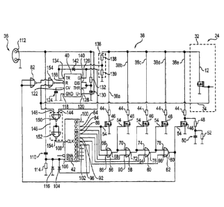
Figure 4 shows a comparatively detailed circuit diagram of disconnecting
device 36, including
phases 38 connected in parallel to switch 32. Voltage limiter 36 has a first
phase 38a, a second
phase 38b, a third phase 38c, a fourth phase 38d and a fifth phase 38e, which
are connected in
parallel to each other and in parallel to switch 32. For example, one of the
terminals of switch 32
is routed to ground, so that all phases 38a, 38b, 38c, 38d, 38e are also
routed to ground.
Phases 38 are of the same design and each include a resistor 44 and a
switching element 46 in
the form of an IGBT. In summary, each of phases 38 has one of switching
elements 46.
Resistor 44 and switching element 46 of each phase 38 are connected in series
to each other.
The ohmic resistance of individual phases 38a, 38b, 38c, 38d, 38e is at least
partially increased
by an integral multiple in each case. The ohmic resistance of resistor 44 of
first phase 38a is 20
ohms, the ohmic resistance of resistor 44 of second phase 38b is 40 ohms, the
ohmic
resistance of resistor 44 of third phase 38c is 80 ohms, and the ohmic
resistance of resistor 44
of fourth and fifth phases 38d, 38e is 160 ohms in each case. A series
connection of a further
CA 03034954 2019-02-25
17
resistor 48 and a capacitor 50 in the form of a condenser is connected in
parallel to switching
element 46 of fifth phase 38e. Capacitor 50 is routed to the potential of one
of the terminals of
switch 32, i.e. to ground. Capacitor 50 itself is bridged by an additional
resistor 52, which is
consequently connected in parallel to capacitor 50. Then ohmic resistance of
further resistor 48
is equal to the ohmic resistance of resistor 44 of fifth phase 38e and is 160
ohms. The ohmic
resistance of additional resistor 52 is, for example, 1 Mohm.
Each switching element 46 has a control input 54, with the aid of which the
switching state of
particular switching element 46 may be set. If switching element 46 is set
with the aid of control
input 54 in such a way that the it is in an electrically non-conductive state,
a current flow across
this particular phase 38 is prevented. Voltage limiter 36 includes a first OR
logic switch 56, a
second OR logic switch 58, a third OR logic switch 60 and a fourth OR logic
switch 62, which
are OR gates in each case. Control input 54 of switching element 46 of first
phase 38a is routed
to a first output 64 of shift register 42 as well as to a first input 66 of
first OR logic switch 56.
Control input 54 of switching element 46 of second phase 38b is routed to an
output 68 of first
logic switch 56 as well as to a first input 70 of second OR logic switch 58.
Control input 54 of
switching element 46 of third phase 38c is routed to an output 72 of second OR
logic switch 58
as well as to a first input 72 of third OR logic switch 60. Control input 54
of switching element 46
of fourth phase 38d is routed to an output 76 of third OR logic switch 60 as
well as to a first input
78 of fourth OR logic switch 62. Control input 54 of switching element 46 of
fifth phase 38e is
routed to an output 80 of fourth OR logic switch 62 as well as to both inputs
of a first NOR gate
82.
A second output 84 of shift register 42 is routed to a second output 86 of
first OR logic switch
56. A third output 88 of shift register 42 is routed to a second output 90 of
second OR logic
switch 58. A fourth output 92 of shift register 42 is routed to a second
output 94 of third OR logic
switch 60. A fifth output 96 of shift register 42 is routed to a second output
98 of fourth OR logic
switch 62. OR logic switches 56, 58, 58, 60, 62 are of the same design.
Moreover, a level is
present at each of particular outputs 68, 72, 76, 80 when a level is present
at at least one of
inputs 66, 68 or 70, 90 or 74, 94 or 78, 98.
A start output 100 of shift register 42 is free and therefore not electrically
contacted with any
other electric or electronic component. End output 102 of shift register 42 is
routed to a reset
input 106 of shift register 42 via a first diode 104. Only a current flow from
end output 102 to
, CA 03034954 2019-02-25
=
18
reset input 106 is facilitated by means of diode 104. If shift register 42 is
activated, start output
100 is driven first. First output 64, second output 84, third output 88,
fourth output 92 and fifth
output 96 are subsequently driven, followed by end output 102, the driving
taking place as a
function of a driving signal present at a time input 108. Start output 100
this corresponds to
channel QO, first output 64 corresponds to channel 01, second output 84
corresponds to
channel 02, etc. up to end output 102, which corresponds to channel 06.
Reset input 106 of shift register 42 is routed via a second capacitor 110 to a
power supply
source 112, with the aid of which a direct current of 15 volts is provided.
Reset input 106 is also
routed to ground via a second resistor 114. A second diode 116 is connected in
parallel to
second resistor 114, with the aid of which a current flow from ground to reset
input 106 is
facilitated.
Timer 40 is connected as a monostable flip-flop. A GND terminal 118 is thus
routed to ground,
and a supply voltage terminal 120 is routed to power supply source 112. A
control terminal 122
is routed to ground via a third capacitor 124. A discharge terminal 126 is
routed to a threshold
terminal 128 as well as to ground via a fourth capacitor 130. Discharge
terminal 126 and
threshold terminal 128 are also routed to power supply source 112 with the aid
of a third resistor
132. A trigger terminal 134 is electrically contacted with electric line 12
with the aid of a voltage
divider 136. For this purpose, trigger terminal 134 is routed to electric line
12 with the aid of a
fourth resistor 138 and to ground with the aid of a fifth resistor 139.
A time output 140 of timer 40 is routed to trigger terminal 134 with the aid
of a third diode 142, a
current flow to trigger terminal 134 at time output 140 being facilitated.
Time output 140 is
furthermore routed to a second input 144 of a logic switch 146. A first input
148 of logic switch
146 is routed to control input 34 of switch 32. Logic switch 146 has a second
NOR gate 150,
whose inputs form inputs 144, 148 of logic switch 146. The output of second
NOR gate 150 is
routed to the two inputs of a third NOR gate 152. The output of third NOR gate
152 forms an
output 154 of logic switch 146, which is routed to time input 108 of shift
register 42. As a result,
output 154 of logic switch 148 has a level precisely when a level (signal) is
present at either first
input 148 or second input 144 of logic switch 146. In summary, time input 108
of shift register 42
is operatively connected to control input 34 of switch 32. Control input 34 is
also routed to an
input of a fourth NOR gate 154, whose other input is routed to the output of
first NOR gate 82.
The output of fourth NOR gate is routed to a reset terminal 156 of timer 40.
CA 03034954 2019-02-25
19
Figure 5 shows a method 158 for operating disconnecting device 24. In a first
work step 160, a
level is applied to reset input 106 of shift register 42 with the aid of power
supply source 112, so
that start output 100 is driven. In summary, an electrical voltage is present
at power supply
source 112, and a signal is therefore also present at reset input 106 of shift
register 42 and start
output 100 is therefore then driven. As a result, all switching elements 46
are blocked, and
essentially no current flow is possible across voltage limiter 36. Switch 32
is in the open state,
and no electrical current may flow across disconnecting device 24.
In a subsequent second work step 162, switch 32 is driven in such a way that
it closes. As a
result, a signal is present at control input 34, which activates timer 40. Due
to logic switch 146, a
level is thus present at time input 108 of shift register 42, and first output
64 is therefore driven.
As a result, all switching elements 46 of phases 38 are driven due to OR logic
switches 56, 58,
60, 62, so that they are electrically conductive. However, they have a higher
ohmic resistance,
compared to switch 32, so that electrical current essentially flows only
across switch 32. Due to
first NOR gate 82 and fourth NOR gate 154, timer 40 is held in a reset state,
and it is ensured
that timer 40 is activated only when switch 32 is in an open position, i.e. is
electrically non-
conductive.
In third work step 164, switch 32 is opened, so that no signal is present
anymore at control
input 34. As a result, the electrical current fully commutates to phases 38,
so that an electrical
current continues to flow across disconnecting device 24 even if a load is
inductively connected
to electric line 12, and a formation of a comparatively high electrical
voltage at switch 32 is thus
prevented. Since the ohmic resistance of voltage limiter 36 is increased
compare to the ohmic
resistance of switch 32, an electrical voltage arising across voltage divider
136 increases. The
present electrical voltage is applied to trigger terminal 134 of timer 40 with
the aid of voltage
divider 136. Once this electrical voltage has dropped to one third of the
operating voltage, a
pulse is output across time output 140 after a certain period of time and
conducted to logic chip
146. As a result, shift register 42 is controlled and its second output 84 is
now driven. As a
result, switching element 46 of first phase 38a is switched to the
electrically non-conductive
state, whereupon remaining switching elements 46 of remaining phases 38b, 38c,
38d and 38e
remain electrically conductive. As a result, the electrical resistance of
voltage limiter 36 is
increased. The electrical voltage present at trigger terminal 134 of timer 40,
in turn, therefore
increases. It drops and once it again is one third of the operating voltage of
timer 40, a pulse is
CA 03034954 2019-02-25
again conducted to logic chip 146 with the aid thereof after certain periods
of time in each case
in additional work steps, so that third output 88 or fourth output 92 is now
driven, and switching
element 46 of second phase 38b or third phase 38c is therefore also now
switched to the non-
conductive state. Since the ohmic resistance of phases 38a, 38b, 38c, 38d, 38e
is a least
partially successively increased, the continuing electrical current
comparatively significantly
decreases.
To ensure a safe driving of shift register 42 even under weak inductive loads,
timer 40 is
connected as a monostable flip-flop. The minimum pulse width is determined
with the aid of
third resistor 132 and fourth capacitor 130. Fourth capacitor 130 is charged
with the aid of third
resistor 132 when a signal is present at time output 140. This takes place
until the voltage
present at threshold terminal 128 is less than 2/3 of the operating voltage.
Since a new pulse
may only begin when the electrical voltage at trigger terminal 134 has dropped
below 1/3 of the
operating voltage, the time output is coupled back to trigger terminal 134
with the aid of third
diode 142.
When fifth output 96 of shift register 42 is driven, only switching element 46
of fifth phase 38e is
switched to the electrically conductive state, and voltage limiter 36
therefore essentially has the
ohmic resistance of resistor 44 of fifth phase 38e. If a pulse is now applied
to time input 108 of
shift register 42 in a final work step 166, end output 102 is driven. As a
result, reset terminal 106
of shift register 42 is driven and consequently reset, so that start output
100 is driven. All
switching elements 46 of phases 38 are also now switched to the electrically
non-conductive
state. As a result, the RC circuit, which is formed from additional resistor
48 and capacitor 50 as
well as partially with the aid of capacitor 44 of fifth phase 38e, absorbs the
remaining inductively
stored electrical energy, so that the electrical current flowing across
voltage limiter 36 is forced
to zero. A discharge of capacitor 50 is ensured with the aid of additional
resistor 52.
In summary, the electrical resistance of voltage limiter 36 is successively
increased over time
with the aid of shift register 42, an increase taking place only if the
flowing electrical current is
below a certain limiting value. This limiting value is set with the aid of
resistors 44. As a result, a
formation of a comparatively high electrical voltage is prevented when switch
32 is actuated,
even under a comparatively pronounced inductive load and thus a comparative
continuation of
an electrical current flow. If a comparatively high current flow continues,
the electrical resistance
is comparatively low, so that the electrical voltage is comparatively low.
Only when the electrical
. CA 03034954 2019-02-25
,
21
current is below a limiting value is the electrical resistance increased,
which also increases the
resulting electrical voltage. Once the electrical current has decreased
again¨and consequently
also the present electrical voltage¨is the electrical resistance, in turn,
increased, so that the
electrical voltage is again increased. As a result, the electrical current
flow is again further
reduced to an increasing degree.
The invention is not limited to the exemplary embodiment described above.
Instead, other
variants of the invention may be derived herefrom by those skilled in the art
without going
beyond the subject matter of the invention. Moreover, in particular, all
individual features
described in connection with the exemplary embodiment may also be otherwise
combined with
each other without going beyond the subject matter of the invention.
CA 03034954 2019-02-25
22
List of Reference Numerals
2 motor vehicle
4 drive wheel
6 wheel
8 electric motor
high-voltage battery
12 electric line
14 high-voltage vehicle electrical system
16 circuit breaker
18 low-voltage vehicle electrical system
low-voltage battery
22 actuator
24 disconnecting device
26 control unit
28 sensor
interface
32 switch
34 control input
36 voltage limiter
38 phase
38a first phase
38b second phase
38c third phase
38d fourth phase
38e fifth phase
timer
42 shift register
44 resistor
46 switching element
48 further resistor
capacitor
52 additional resistor
54 control input
CA 03034954 2019-02-25
23
56 first OR logic switch
58 second OR logic switch
60 third OR logic switch
62 fourth OR logic switch
64 first output of the shift register
66 first input of the first OR logic switch
68 output of the first OR logic switch
70 first input of the second OR logic switch
72 output of the second OR logic switch
74 first input of the third OR logic switch
76 output of the third OR logic switch
78 first input of the fourth OR logic switch
80 output of the fourth OR logic switch
82 first NOR gate
84 second output of the shift register
86 second input of the first OR logic switch
88 third output of the shift register
90 second input of the second OR logic switch
92 fourth output of the shift register
94 second input of the third OR logic switch
96 fifth output of the shift register
98 second input of the fourth OR logic switch
100 start output
102 end output
104 diode
106 reset input
108 time input
110 second capacitor
112 power supply source
114 second resistor
116 second diode
118 GND terminal
120 supply voltage terminal
122 control terminal
= CA 03034954 2019-02-25
24
124 third capacitor
126 discharge terminal
128 threshold terminal
130 fourth capacitor
132 third resistor
134 trigger terminal
136 voltage divider
138 fourth resistor
139 fifth resistor
140 time output
142 third diode
144 second input of the logic switch
146 logic switch
148 first input of the logic switch
150 second NOR gate
152 third NOR gate
154 fourth NOR gate
156 reset terminal
158 method
160 first work step
162 second work step
164 third work step
166 final work step