Note: Descriptions are shown in the official language in which they were submitted.
CA 03034996 2019-02-25
1
DESCRIPTION
SECONDARY BATTERY
TECHNICAL FIELD
[0001]
The embodiments described herein relate to a secondary
battery.
BACKGROUND ART
[0002]
As conventional secondary batteries, there have been
proposed secondary batteries, in which a first electrode / an
insulating material / an n type oxide semiconductor layer / a p
type oxide semiconductor layer / a second electrode are layered,
since electrolytic solutions and rare elements are not used and
thinning thereof can be realized.
[0003]
Moreover, as a structure similar to such secondary batteries,
.. there have been proposed secondary batteries including: a positive
electrode including a positive-electrode active material layer
containing a nickel oxide or the like as a positive-electrode
active material; a solid electrolyte having an aqueous porous
structure; and a negative electrode including a
negative-electrode active material layer containing a titanium
oxide or the like as a negative-electrode active material.
[0004]
JMJCN-171-PCT-CA_Specification
CA 03034996 2019-02-25
2
Patent Literature 1: Japanese Patent No. 5508542
Patent Literature 2: Japanese Patent No. 5297809
Patent Literature 3: Japanese Patent Application Laid-Open
Publication No. 2015-82445
Patent Literature 4: Japanese Patent Application Laid-Open
Publication No. 2016-82125
SUMMARY OF INVENTION
Technical Problem
[0005]
The embodiments provide a highly reliable secondary battery
capable of improving an energy density and increasing battery
characteristics (electricity accumulation capacity).
Solution to Problem
[0006]
According to one aspect of the embodiments, there is
provided a secondary battery comprising: a first oxide
semiconductor having a first conductivity type; a first charging
layer disposed on the first oxide semiconductor layer, the first
charging layer composed by comprising a first insulating material
and a second oxide semiconductor, the second oxide semiconductor
having the first conductivity type; a third oxide semiconductor
layer having a second conductivity type disposed on the first
charging layer; and a hydroxide layer disposed between the first
charging layer and the third oxide semiconductor layer , the
hydroxide layer containing a hydroxide of a metal constituting
JMJCN-171-PCT-CA_Specification
CA 03034996 2019-02-25
3
the third oxide semiconductor layer.
Advantageous Effects of Invention
[0007]
According to the embodiments, there can be provided the
highly reliable secondary battery capable of improving the energy
density and increasing the battery characteristics (electricity
accumulation capacity).
BRIEF DESCRIPTION OF THE DRAWINGS
[0008]
[Fig. 1] A schematic cross-sectional structure diagram showing
a secondary battery according to the embodiments.
[Fig. 2] (a) An energy band diagram before charging of the
secondary battery according to the embodiments, and (b) a
schematic configuration diagram of each layer corresponding to
Fig. 2(a).
[Fig. 3] (a) An energy band diagram during charging (forward bias
state) of the secondary battery according to the embodiments, and
(b) a schematic configuration diagram of each layer corresponding
to Fig. 3(a).
[Fig. 4] (a) An energy band diagram in a fully charged state of
the secondary battery according to the embodiments, and (b) a
schematic configuration diagram of each layer corresponding to
Fig. 4(a).
[Fig. 5] (a) An energy band diagram in a discharged state (state
connected to a load) of the secondary battery according to the
JMJCN-171-PCT-CA_Specification
CA 03034996 2019-02-25
4
embodiments, and (b) a schematic configuration diagram of each
layer corresponding to Fig. 5 (a) .
[Fig. 6] (a) An energy band diagram in a fully discharged state
of the secondary battery according to the embodiments, and (b)
a schematic configuration diagram of each layer corresponding to
Fig. 6(a) .
[Fig. 7] (a) A schematic circuit configuration diagram showing
a control system to be applied to an electrical stimulation process
of forming a hydroxide layer between a first charging layer and
a third oxide semiconductor layer in the secondary battery
according to the embodiments, and (b) a waveform example of a pulse
voltage VA to be applied between a first electrode and a second
electrode.
[Fig. 8] A diagram showing an experimental result of a relationship
between an energy density and an electrical stimulation time in
the secondary battery according to the embodiments.
[Fig. 9] An example of a scanning electron microscope (SEM)
photograph of a cross section of a sample in which a second charging
layer is formed by using silicone oil, in the secondary battery
according to the embodiments.
[Fig. 10] An example of an SIMS profile for each element, in the
secondary battery according to the embodiments shown in Fig. 9.
[Fig. 11] A diagram showing a relationship of a resistor R between
the first electrode and the second electrode and an energy density
(a .u. ) with respect to an amount of dosage of a conductivity
adjusting material (a . u. ) , in the secondary battery according to
the embodiments.
JMJCN-171-PCT-CA_Specification
CA 03034996 2019-02-25
DESCRIPTION OF EMBODIMENTS
[0009]
Next, the embodiments will be described with reference to
5 drawings. In the description of the following drawings, the
identical or similar reference sign is attached to the identical
or similar part. However, it should be noted that the drawings
are schematic and therefore the relation between thickness and
the plane size and the ratio of the thickness differs from an actual
thing. Therefore, detailed thickness and size should be
determined in consideration of the following explanation. Of
course, the part from which the relation and ratio of a mutual
size differ also in mutually drawings is included.
[0010]
Moreover, the embodiments shown hereinafter exemplify the
apparatus and method for materializing the technical idea; and
the embodiments do not specify the material, shape, structure,
placement, etc. of each component part as the following. The
embodiments may be changed without departing from the spirit or
scope of claims.
[0011]
[Embodiments]
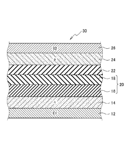
Fig. 1 shows a schematic cross-sectional structure of a
secondary battery according to the embodiments. Hereinafter, a
secondary battery 30 according to the embodiments will be
explained.
MCN-171-PCT-CA_Speafication
CA 03034996 2019-02-25
6
[0012]
As shown in Fig. 1, the secondary battery 30 according to
the embodiments includes: a first oxide semiconductor 14 having
a first conductivity type; a first charging layer 16 disposed on
the first oxide semiconductor layer 14, and composed by including
a first insulating material and a second oxide semiconductor
having the first conductivity type; a third oxide semiconductor
layer 24 having a second conductivity type disposed on the first
charging layer 16; and a hydroxide layer 22 disposed between the
first charging layer 16 and the third oxide semiconductor layer
24, and containing a hydroxide of a metal constituting the third
oxide semiconductor layer 24.
[0013]
Moreover, the secondary battery 30 according to the
embodiments may include a second charging layer 18 disposed
between the first charging layer 16 and the hydroxide layer 22,
as shown in Fig. 1.
[0014]
In the embodiments, the second charging layer 18 may include
a second insulating material.
[0015]
Alternatively, the second charging layer 18 may include the
second insulating material and a conductivity adjusting material.
[0016]
Alternatively, the first charging layer 16 may include a
structure of at least two-layer of which compositions are
different from each other. The first charging layer 16 may be
MCN-171-PCT-CA_Specification
CA 03034996 2019-02-25
7
formed by including a silicon oxide (S102) / a titanium oxide (TiO2),
for example. Specifically, the first charging layer 16 may be
formed by including a layered structure of Si02 / Ti02, or may be
formed by including a particulate bonding structure in which the
periphery of particle-shaped TiO2 is covered with Si02.
Alternatively, the first charging layer 16 may include a structure
into which TiO2 and Si02 are mixed, or a structure in which TiO2
is wrapped in a silicon oxide. In the above description, the
compositions of the titanium oxide and the silicon oxide are
respectively not limited to TiO2 and Si02, but may include a
structure in which the composition ratio x, of TiOx and/or SiOx
is changed.
[0017]
Moreover, the n type oxide semiconductor may be an oxide
of titanium (Ti), tin (Sn), zinc (Zn), or magnesium (Mg).
Accordingly, the first charging layer 16 may be a layered structure
of Si02 and an oxide of with Ti, Sn, Zn, or Mg, or may be formed
of a particulate bonding structure in which the periphery of an
oxide of particle-shaped Ti, Sn, Zn, or Mg is covered with SiO2.
Alternatively, the first charging layer 16 may include a
configuration in which a molecule or molecular group of Si02 and
an oxide of Ti, Sn, Zn, or Mg is surrounded by Si02 (amorphous).
[0018]
Alternatively, the first charging layer 16 may include a
porous structure.
[0019]
Moreover, the second oxide semiconductor may include at
JMJCN-171-PCT-CA_Specification
CA 03034996 2019-02-25
8
least one oxide selected from the group consist of an oxide of
Ti, an oxide of Sn, an oxide of Zn, and an oxide of Mg.
[0020]
Moreover, the conductivity adjusting material may include
an oxide of a semiconductor having the first conductivity type
or an oxide of a metal.
[0021]
Alternatively, the conductivity adjusting material may
include at least one oxide selected from the group of consisting
of an oxide of Sn, an oxide of Zn, an oxide of Ti, and an oxide
of niobium (Nb).
[0022]
More specifically, the second insulating material may
include SiO2 and the conductivity adjusting material may include
SnOx, in the secondary battery 30 according to the embodiments.
[0023]
Alternatively, the second insulating material may include
SiOx formed as a film from silicone oil, in the secondary battery
30 according to the embodiments.
[0024]
Alternatively, the first insulating material may include
5i02 and the second oxide semiconductor may include Ti02, in the
secondary battery 30 according to the embodiments.
[0025]
(Hydroxide Layer)
The hydroxide layer 22 is a layer which reduces a metal
JMJCN-171-PCT-CA_Specification
CA 03034996 2019-02-25
9
hydroxide and converts an electron hole (h+) into a hydrogen ion
(Hi) by an application of an electric field at the time of charging,
and converts the hydrogen ion into the electron hole at the time
of discharging.
[0026]
If the hydroxide is a nickel hydroxide, the following
reaction formula is realized.
[0027]
- Nickel Hydroxide Layer -
The nickel hydroxide (Ni(OH)2) is changed to a nickel
oxyhydroxide (Ni0OH) by the applications of the electric field.
A reaction of Ni(OH)2 + h+ -4 Ni0OH + H+ progresses at the time
of charging, and a reaction of Ni0OH + 1-1+-* Ni(OH)2+h+ progresses
at the time of discharging. The aforementioned reaction causes
electrochromism.
[0028]
(First Charging Layer)
The first charging layer 16 is a layer which is paired with
the hydroxide layer 22 and accumulates hydrogen generated at the
time of charging. In the first charging layer 16, a reaction of
M + H20 + e- MM + OH-
progresses at the time of charging, and
a reaction of MH + OH -* M + H20 + e- progresses at the time of
discharging. If the first charging layer 16 is made porous,
efficiency of accumulating the hydrogen can be increased.
Moreover, the hydrogen accumulation and electrical conductivity
JMJCN-171-PCT-CA_Specification
CA 03034996 2019-02-25
can be optimized if the first charging layer 16 is formed as a
plurality of layers. It can be optimized by forming the second
oxide semiconductor by using an oxide of Ti, Sn, Zn or Mg.
5 [0029]
(Second Charging Layer)
The second charging layer 18 is a buffer layer for adjusting
movement of H+ and electrons (e-). The mobility of H+ and e- can
be further adjusted by adding a conductivity adjusting material.
10 The second charging layer 18 can be thickly formed in a high
breakdown voltage electrically by using an oxide of Sn, Zn, Ti,
or Nb for the conductivity adjusting material.
[0030]
(P type Oxide Semiconductor Layer)
The oxide semiconductor layer 24 constitutes a pn junction
with respect to the n type semiconductor of the hydroxide layer
(Ni0OH of the nickel hydroxide layer) , and can suppress an electric
charge leak at the time of charging. If the p type oxide
semiconductor layer 24 is formed by using NiO, it is possible to
form Ni(OH)2 layer by electrical stimulation.
[0031]
(N type First Oxide Semiconductor Layer)
The n type first oxide semiconductor layer 14 has an electric
resistance intermediate between a first electrode 12 and a first
charging layer 16, and makes electrical bonding smooth.
JMJCN-171-PCT-CA_Specification
CA 03034996 2019-02-25
11
[0032]
As shown in Fig. 1, the secondary battery 30 according to
the embodiments may include the first electrode 12 and the second
electrode 26; the first oxide semiconductor layer 14 may include
an n type first oxide semiconductor layer, and may be connected
to the first electrode 12; the second oxide semiconductor may
include an n type second oxide semiconductor; and the third oxide
semiconductor layer 24 may include a p type third oxide
semiconductor layer, and may be connected to the second electrode
26.
[0033]
Further in details, the third oxide semiconductor layer 24
may include a nickel oxide (NiO), and the hydroxide layer 22 may
include at least any one of a nickel hydroxide (Ni(OH)2) or nickel
oxyhydroxide (Ni0OH), in the secondary battery 30 according to
the embodiments.
[0034]
Alternatively in the secondary battery 30 according to the
embodiments, the third oxide semiconductor layer 24 may include
the nickel oxide (NiO) ; the hydroxide layer 22 may include a
laminated structure in which both of the nickel hydroxide
(Ni(OH)2) and the nickel oxyhydroxide (Ni0OH) are mixed, and the
nickel hydroxide (Ni(OH)2) may be contacted with the third oxide
semiconductor layer 24, and the nickel oxyhydroxide (Ni0OH) may
be contacted with the second charging layer 18.
[0035]
Moreover, in the secondary battery 30 according to the
JMJCN-171-PCT-CA_Specification
CA 03034996 2019-02-25
12
embodiments, the third oxide semiconductor layer 24 includes the
nickel oxide (NiO); and the hydroxide layer 22 includes the nickel
oxyhydroxide (Ni0OH) when fully charged, and includes the nickel
hydroxide (Ni(OH)2) when fully discharged.
[0036]
Furthermore, the nickel hydroxide (Ni(OH)2) is changed to
the nickel oxyhydroxide (Ni0OH) at the time of the charging in
which the second electrode 26 is biased to positive with respect
to the first electrode 12.
[0037]
Moreover, the nickel oxyhydroxide (Ni0OH) is changed to the
nickel hydroxide (Ni(OH)2) at the time of discharging via a load
connected between the first electrode 12 and the second electrode
26.
[0038]
The hydroxide layer 22 may be formed as a film directly on
the second charging layer 18, or may be formed by periodically
applying a pulse voltage between the p type third oxide
semiconductor layer 24 and the n type first oxide semiconductor
layer 14, as mentioned below.
[0039]
An electricity accumulation capacity can be increased by
forming the nickel hydroxide (Ni(OH)2) layer between the charging
layer 20 (the first charging layer 16 + the second charging layer
18) and the third oxide semiconductor layer 24, in the secondary
battery 30 according to the embodiments.
[0040]
MCN-171-PCT-CA_Specification
CA 03034996 2019-02-25
13
Moreover, in the secondary battery 30 according to the
embodiments, there maybe adopted a configuration in which a layer
containing many OH groups (Ni(OH)x), Si(OH)x is formed to be
inserted between the second charging layer 18 and the p type third
oxide semiconductor layer 24. The electricity accumulation
capacity can be enlarged by including such a configuration, and
thereby battery performance can be improved. More specifically,
the hydroxide layer 22 is not limited to the nickel hydroxide
(Ni(OH)2), but may be formed as a mixture layer, e.g. the layer
containing many OH groups (Ni(OH)x), Si(OH)x. A compound of Ni,
Si, 0, H and elements which constitutes the second charging layer
18 may be contained as a structural factor.
[0041]
(Energy Band Diagram)
Hereinafter, there will be described an example in which
the p type third oxide semiconductor layer 24 is formed of the
nickel oxide (NiO) , the hydroxide layer 22 is formed of at least
any one of the nickel hydroxide (Ni(OH)2) or the nickel
oxyhydroxide (Ni0OH), the first charging layer 16 is formed of
SiO2/TiO2, and the second charging layer 18 is formed of Si02/SnO.
[0042]
- Before Charging -
Fig. 2(a) A shows an energy band diagram before charging
of the secondary battery 30 according to the embodiments, and Fig.
2(b) shows a schematic configuration of each layer corresponding
JMJCN-171-PCT-CA_Specification
CA 03034996 2019-02-25
14
to Fig. 2(a). In the drawings, Ef denotes the Fermi level.
[0043]
The p type third oxide semiconductor layer 24 which is the
nickel oxide (NiO) is connected to a second electrode (26) E2,
and the first charging layer 16 which is SiO2 / TiO2 is connected
to a first electrode (12) El.
[0044]
In a thermal equilibrium state, the energy band diagram
before charging of the secondary battery 30 according to the
embodiments is shown, as shown in Fig. 2(a), a conduction band
of NiO / Ni(OH)2 / SnO / TiO2 exists in a level of 1.8 eV / 1.47
eV / 4.3 to 4.5 eV / 4.3 eV with respect to the vacuum level.
Moreover, the bandgap energy Eg of NiO / Ni(OH)2 / SnO / TiO2 is
4.0 eV / 3.7 eV / 3.8 eV / 3.2 eV. Moreover, the bandgap energy
Eg of SiO2 which constitutes the charging layer 20 is 8.9 eV.
Before charging, the hydroxide layer 22 is the nickel hydroxide
(Ni(OH)2)=
[0045]
- During Charging (Forward Bias State) -
Fig. 3(a) shows an energy band diagram in during charging
(forward bias state) of the secondary battery 30 according to the
embodiments, and Fig. 3(b) shows a schematic configuration of each
layer corresponding to Fig. 3(a).
[0046]
Fig. 3(a) shows the energy band diagram in a state where
the second electrode E2 is connected to plus (+), the first
JMJCN-171-PCT-CA_Specification
CA 03034996 2019-02-25
electrode El is connected to minus (-), and a charging voltage
of, for example, approximately 2.8V is applied. In this context,
the Fermi level Ef in a state of applying approximately 2.8V is
expressed as shown in Fig. 3(a).
5 [0047]
Since the nickel oxyhydroxide (Ni0OH) is generated from the
nickel hydroxide (Ni(OH)2) in the hydroxide layer 220 during
charging in the secondary battery 30 according to the embodiments,
the hydroxide layer 22C during charging is represented by a layered
10 structure of the nickel hydroxide (Ni(OH)2) / the nickel
oxyhydroxide (Ni0OH), as shown in Figs. 3(a) and 3(b). The nickel
hydroxide (Ni(OH)2) layer is mainly disposed at the nickel oxide
layer (NiO) side, and the nickel oxyhydroxide (Ni0OH) layer is
disposed at the second charging layer 18 side.
15 [0048]
Since approximately 2.8V is applied as a positive voltage
between the second electrode E2 and the first electrode El during
charging, an electron e- is injected into the n type oxide
semiconductor (TiO2) of the charging layer 20 from the first
electrode El, and a hole 1-1+ is injected into the p type oxide
semiconductor layer (NiO) 24 from the second electrode E2, inside
the secondary battery 30.
[0049]
Due to assist of water or water vapor component (H20), an
reaction of Ni(OH)2 + OH- -* Ni0OH + H20 +e- progresses at the
positive electrode side, whereas an reaction of M + H20 +e- -* NH
+ 0H progresses at the negative electrode side. In this context,
JMJCN-171-PCT-CA_Speafication
CA 03034996 2019-02-25
16
M denotes a metallic element in the charging layer 20.
[0050]
As a result, since a reaction of Ni(OH)2 + h+ -* Ni0OH + H+
progresses in the hydroxide layer 220 during the charging,
hydrogen accumulation due to the assist of the water or water vapor
component (H20) is realized in the charging layer 20 in accordance
with the synthesis between the hydrogen ion H+ and the electron
e-, as shown in Fig. 3(a). In this case, the hydrogen His coupled
to dangling bonds of Ti, Si, etc., in the charging layer 20, in
the hydrogen accumulation. It is also possible to be coupled in
OH form.
[0051]
- Full Charge -
Fig. 4(a) shows an energy band diagram in a fully charged
state of the secondary battery 30 according to the embodiments,
and Fig. 4(b) shows a schematic configuration of each layer
corresponding to Fig. 4(a). A conduction band of NiO / Ni0OH
exists at a level of 1.8eV + 2.8 eV / eV + 2.8eV with respect
to the vacuum level. Moreover, the bandgap energy Eg of Ni0OH is
1.75 eV.
[0052]
In an opened state after full charging in which fully
hydrogen accumulation is performed in the charging layer 20, a
holding voltage slightly lower than that at the time of the
charging (2.8V) is held between the second electrode E2 and the
first electrode El.
JMJCN-171-PCT-CA_Specification
CA 03034996 2019-02-25
17
[0053]
Moreover, in the fully charged state of the secondary
battery 30 according to the embodiments, the nickel hydroxide
(Ni(OH)2) layer 22 is changed to the nickel oxyhydroxide (Ni0OH)
layer 22F, and then energy accumulation as chemical potential of
unstable Ni0OH is performed.
[0054]
- During Discharging -
Fig. 5(a) shows an energy band diagram in a discharged state
(state connected to a load) of the secondary battery 30 according
to the embodiments, and Fig. 5(b) shows a schematic configuration
of each layer corresponding to Fig. 5(a). More specifically, the
energy band diagram in the discharged state (state connected to
the load) where a load 42 is connected between the second electrode
E2 and the first electrode El is expressed as shown in Fig. 5(a).
In this case, the Fermi level Ef in a state of applying
approximately 2.8V gradually increases in accordance with a
discharged state, as shown in Fig. 5(a). In the discharged state
(state connected to the load) of the secondary battery 30 according
to the embodiments, the reverse reaction of the above-mentioned
charging operation occurs.
[0055]
Since the nickel hydroxide (Ni(OH)2) is generated from the
nickel oxyhydroxide (Ni0OH) in the hydroxide layer 220 during
discharging, in the secondary battery 30 according to the
embodiments, the hydroxide layer 22D during discharging is
JMJCN-171-PCT-CA_Specification
CA 03034996 2019-02-25
18
represented by a layered structure of the nickel hydroxide
(Ni(OH)2) / the nickel oxyhydroxide (Ni0OH), as shown in Figs.
5(a) and 5(b). The nickel hydroxide (Ni(OH)2) layer is mainly
formed at the nickel oxide layer (NiO) side, and the nickel
oxyhydroxide (Ni0OH) layer is formed at the second charging layer
18 side.
[0056]
Since the load 42 is externally connected between the second
electrode E2 and the first electrode El during discharging, the
electron e- is discharged to the first electrode El from the n
type oxide semiconductor (Ti02) of the charging layer 20, and the
hole h+ is discharged to the second electrode E2 from the p type
oxide semiconductor layer (Ni0) 24, inside the secondary battery
30.
[0057]
Due to assist of water or water vapor component (H20), an
reaction of Ni0OH + H20 + e- Ni(OH)2
+ OH- progresses at the
positive electrode side, whereas an reaction of MH + OH- M +
H20 + e- progresses at the negative electrode side.
[0058]
As a result, since a reaction of Ni0OH + H+ Ni(OH)2
+ h+
progresses in the hydroxide layer 22D during the discharging,
release of the hydrogen accumulation state due to the assist of
the water or water vapor component (H20) is realized in the charging
layer 20 in accordance with separation between the hydrogen ion
H+ and the electron e-, as shown in Fig. 5(a).
JMJCN-171-PCT-CA_Specification
CA 03034996 2019-02-25
19
[0059]
- Fully Discharged State -
Fig. 6(a) shows an energy band diagram in a fully discharged
state of the secondary battery 30 according to the embodiments,
and Fig. 6(b) shows a schematic configuration of each layer
corresponding to Fig. 6(a).
[0060]
In the fully discharged state, the nickel oxyhydroxide
(Ni0OH) is changed to the nickel hydroxide (Ni(OH)2) layer 22.
[0061]
In the fully discharged state, the energy band diagram of
the secondary battery 30 according to the embodiments is expressed
as shown in Fig. 6(a), and a conduction band of NiO / Ni(OH)2 /
SnO / TiO2 exists in a level of 1.8 eV / 1.47 eV / 4.3 to 4.5 eV
/ 4.3 eV with respect to the vacuum level. Moreover, the bandgap
energy Eg of NiO / Ni(OH)2 / SnO / TiO2 is 4.0 eV / 3.7 eV / 3.8
eV / 3.2 eV. Moreover, the bandgap energy Eg of SiO2 which
constitutes the charging layer 20 is 8.9 eV. In the fully
discharged state, the hydroxide layer 22 is the nickel hydroxide
(Ni(OH)2)=
[0062]
In the fully discharged state, it has recovered to a state
equivalent to the above-mentioned thermal equilibrium state
before the charging.
[0063]
JMJCN-171-PCT-CA_Specification
CA 03034996 2019-02-25
(Fabrication Method)
A fabrication method of the secondary battery 30 according
to the embodiments includes: forming a first oxide semiconductor
14 having a first conductivity type; forming a first charging layer
5 16 composed by including a first insulating material and a second
oxide semiconductor having the first conductivity type on the
first oxide semiconductor layer 14; forming a second charging
layer 18 on the first charging layer 16; forming a third oxide
semiconductor layer 24 having a second conductivity type on the
10 second charging layer 18; and forming a hydroxide layer 22
containing a hydroxide of a metal constituting the third oxide
semiconductor layer 24 between the first charging layer 16 and
the third oxide semiconductor layer 24.
15 [0064]
- n type Oxide Semiconductor Layer 14 -
A TiO2 layer is formed as a film on the first electrode 12
which constitutes a lower electrode, for example by a sputtering
deposition method. In this case, Ti or TiO can be used as a target.
20 The layer thickness of the n type oxide semiconductor layer 14
is approximately 50 nm to approximately 200 nm, for example. A
tungsten (W) electrode or the like can be applied to the first
electrode 12, for example.
[0065]
- First Charging Layer 16 -
A chemical solution is formed by stirring titanium fatty
MCN-171-PCT-CA_Specification
CA 03034996 2019-02-25
21
acid and silicone oil with a solvent. The aforementioned chemical
solution is coated on the n type oxide semiconductor layer 14 by
means of a spin coater. . The rotational frequency thereof is
approximately 500 to approximately 3000 rpm. It is dried on a
hot plate after the coating. The drying temperature on the hot
plate is approximately 30 C to approximately 200 C, for example,
and the drying time thereon is approximately 5 minutes to
approximately 30 minutes, for example. It is fired after the
drying. In the firing performed after the drying, it is fired
in the atmosphere using a baking furnace. The firing temperature
is approximately 300 C to approximately 600 C, and the firing time
is approximately 10 minutes to approximately 60 minutes.
[0066]
Consequently, aliphatic acid salt is decomposed and then
a fine particle layer of a titanium dioxide covered with a silicone
insulating film is formed. The above-mentioned fabrication
(preparation) method of forming the titanium dioxide layer covered
with the silicone insulating film is a coating and
thermodecomposition method. More specifically, the
aforementioned layer has a structure where a metallic salt of the
titanium dioxide coated with silicone is embedded in the silicone
layer. After the firing, UV irradiation by means of a low pressure
mercury lamp is implemented. The UV irradiation time is
approximately 10 minutes to approximately 100 minutes.
[0067]
JMJCN-171-PCT-CA_Specification
CA 03034996 2019-02-25
22
- Second Charging Layer (Buffer Layer) 18 (Method 1) -
A chemical solution is formed by stirring tin fatty acid
and silicone oil with a solvent. The aforementioned chemical
solution is coated on the first charging layer 16 by means of the
spin coater. The rotational frequency thereof is approximately
500 to approximately 3000 rpm. It is dried on a hot plate after
the coating. The drying temperature on the hot plate is
approximately 30 C to approximately 200 C, for example, and the
drying time thereon is approximately 5 minutes to approximately
30 minutes, for example. Furthermore, it is fired after the
drying. In the firing performed after the drying, it is fired
in the atmosphere using a baking furnace. The firing temperature
is approximately 300 C to approximately 600 C, and the firing time
is approximately 10 minutes to approximately 60 minutes. After
the firing, UV irradiation by means of a low pressure mercury lamp
is implemented. The UV irradiation time is approximately 10
minutes to approximately 100 minutes. The layer thickness of the
second charging layer (buffer layer) 18 after the UV irradiation
is approximately 100 nm to approximately 300 nm, for example.
[0068]
- Second Charging Layer (Buffer Layer) 18 (Method 2) -
A chemical solution is formed by stirring silicone oil with
a solvent. The aforementioned chemical solution is coated on the
first charging layer 16 by means of the spin coater. The
rotational frequency thereof is approximately 500 to
approximately 3000 rpm. It is dried on a hot plate after the
JMJCN-171-PCT-CA_Specification
CA 03034996 2019-02-25
23
coating. The drying temperature on the hotplate is approximately
50 C to approximately 200 C, for example, and the drying time
thereon is approximately 5 minutes to approximately 30 minutes,
for example. Furthermore, it is fired after the drying. In the
firing performed after the drying, it is fired in the atmosphere
using a baking furnace. The firing temperature is approximately
300 C to approximately 600 C, and the firing time is approximately
minutes to approximately 60 minutes. After the firing, UV
irradiation by means of a low pressure mercury lamp is implemented.
10 The UV irradiation time is approximately 10 minutes to
approximately 60 minutes. The layer thickness of the second
charging layer (buffer layer) 18 after the UV irradiation is
approximately 10 nm to approximately 100 nm, for example.
[0069]
- p type Third Oxide Semiconductor Layer 24 -
A NiO layer is formed as a film on the second charging layer
18, for example by a sputtering deposition method. In this case,
Ni or NiO can be used as a target. The layer thickness of the
p type oxide semiconductor layer 24 is approximately 200 nm to
approximately 1000 nm, for example.
[0070]
- Second Electrode 26 -
The second electrode 26 as an upper electrode is formed by
forming Al as a film by means of a sputtering deposition method
or a vacuum evaporation method, for example. The second electrode
JMJCN-171-PCT-CA_Specification
CA 03034996 2019-02-25
24
26 can be formed on the p type third oxide semiconductor layer
(NiO) 24 using Al target. The second electrode 26 may be formed
only on a specified region using a stainless steel mask, for
example.
[0071]
- Ni(OH)2 -
It is formed through an electrical stimulation process which
performs an electrical treatment after the formation of the second
electrode 26.
[0072]
Plus and negative voltages are alternately applied to the
second electrode 26, using the first electrode 12 as a ground
(earth) potential. An atmosphere is the atmospheric air and
humidity is approximately 20% to approximately 60%, for example.
[0073]
Fig. 7(a) shows a schematic circuit configuration of a
control system to be applied to the electrical stimulation process
for forming a hydroxide layer between the charging layer 20 and
the third oxide semiconductor layer 24, in the secondary battery
according to the embodiments. Fig. 7(b) shows a waveform
example of a pulse voltage VA to be applied between the first
electrode 12 and the second electrode 26. In Fig. 7(a), a
connecting relationship between the circuits is expressed by the
25 thick line and a signal flow is expressed by the thin line.
[0074]
As shown in Fig. 7(a), the pulse voltage VA to be applied
MCN-171-PCT-CA_Specification
CA 03034996 2019-02-25
to the second electrode 26 of the secondary battery 30 with which
the first electrode 12 is grounded (earthed) is supplied from a
voltage source 32 through an ammeter 34, a voltmeter 36, and a
resistor 38. The voltage source 32 can be controlled by the
5 control device 40. Moreover, since a value of the ammeter 34 and
a value of the voltmeter 36 are fed back to the control device
40, the pulse voltage VA shown in Fig. 7(b) can be supplied from
the voltage source 32 controlled by the control device 40.
[0075]
10 As shown in Fig. 7(b), one cycle TO is set to 3V (5 seconds)
-* -3V (2 seconds) -* 5V (0.5 seconds) -* -0.4V (4.5 seconds), for
example, and the pulse voltage VA is applied thereto in
approximately 300 to approximately 5000 cycles. Thereby, the
Ni(OH)2 layer 22 can be formed between the second charging layer
15 18 and the third oxide semiconductor layer (NiO) 24. In addition,
it is detected from a measured result of a Secondary Ion Mass
Spectroscopy (SIMS) that substances containing Si, 0, H, and Ni
also exists in the Ni(OH)2 layer 22.
[0076]
20 Also in a structure including only the first charging layer
16 and not including the second charging layer 18 as the charging
layer 20, the hydroxide layer can be formed between the first
charging layer 16 and the third oxide semiconductor layer 24
through the above-mentioned electrical stimulation process.
25 [0077]
The pulse voltage waveform shown in Fig. 7(b) is merely one
example, and the voltage, the number of pulses per cycle, the order
JMJCN-171-PCT-CA_Specification
CA 03034996 2019-02-25
26
of the positive / negative voltages, and the like can be
appropriately selected in accordance with the configuration of
the secondary battery 30. It is also possible to select a pulse
waveform applying of no negative voltage.
[0078]
(Relationship between Energy Density and Electrical Stimulation
Time)
Fig. 8 shows an experimental result of a relationship
between an energy density and an electrical stimulation time, in
the secondary battery 30 according to the embodiments. In the
embodiments, the electrical stimulation time corresponds to a time
period of applying the pulse voltage VA of one cycle TC = 12 seconds
for a plurality of the cycles.
[0079]
As shown in Fig. 8, there is a tendency that the energy
density increases as the electrical stimulation time increases.
It is confirmed that the layer thickness of the hydroxide (Ni (OH) x)
layer 22 increases with elapsing of the electrical stimulation
time.
[0080]
In embodiments, the nickel hydroxide (Ni(OH)2) layer 22 is
formed between the charging layer 20 and the third oxide
semiconductor layer (NiO) 24. As a result, since the reaction of
Ni(OH)2 + h+-+ Ni0OH + W progresses at the time of charging, and
the reaction of Ni0OH + W Ni(OH)2 + h+ progresses at the time
of discharging, there can be provided the secondary battery 30
JMJCN-171-PCT-CA_Specification
CA 03034996 2019-02-25
27
with the increased electricity accumulation capacity.
[0081]
(Experimental Results)
Fig. 9 shows an example of a cross section SEM photograph
of a sample in which the second charging layer 18 is made only
using silicone oil and is subjected to the electrical stimulation
process, in the secondary battery 30 according to the embodiments.
[0082]
The hydroxide (Ni(OH)2) layer 22 is clearly formed between
the second charging layer (buffer layer) 18 and the third oxide
semiconductor layer (NiO) 24 which are formed only of silicone
oil.
.. [0083]
(SIMS Analysis)
In the secondary battery 30 according to the embodiments
shown in Fig. 9, mass spectrometry of each element is implemented
by digging from a front side surface of the third oxide
semiconductor layer (NiO) 24 to obtain an SIMS profile for each
element.
[0084]
In the sample not subjected to the electrical stimulation
process (curved line WO in Fig. 10), a region having a peak of
Si near the depth 5 (a.u.) corresponds to the second charging layer
(buffer layer) 18 made by only using the silicone oil. A peak
of H is observed at an interface between the buffer layer 18 and
JMJCN-171-PCT-CA_Specification
CA 03034996 2019-02-25
28
the third oxide semiconductor layer (NiO) 24 (a portion of which
the depth is the vertical line A).
[0085]
On the other hand, in a sample which subjected to the
electrical stimulation process (the curved line W in Fig. 10),
there is a region with a large amount of H in a depth portion on
the left-hand side of the vertical line A, and therefore it is
estimated it is due to the presence of the hydroxide (Ni(OH)2)
layer 22.
[0086]
The hydroxide (Ni(OH)2) layer 22 is a layer
electrochemically formed through the electrical stimulation
process. Therefore, there is also introduction of Si from SiOx
of the underlying second charging layer (buffer layer) 18, and
the presence of Si can be confirmed also from the SIMS profile
(the curved line W in Fig. 10).
[0087]
Fig. 11 shows a relationship of the resistor R between the
first electrode and the second electrode and an energy density
(a.u.) with respect to an amount of dosage of a conductivity
adjusting material (a.u.), in the secondary battery 30 according
to the embodiments. The energy density (a. u.) corresponds to
the discharge capacity of the secondary battery 30.
[0088]
In Fig. 11, the amount of dosage of conductivity adjusting
material corresponds to a value related to an additive amount of
SnOx in the second charging layer (buffer layer) 18. As shown in
JMJCN-171-PCT-CA_Specification
CA 03034996 2019-02-25
29
Fig. 11, the optimum values of the resistor R between the first
electrode and the second electrode (a.u.) and the energy density
(a.u.) exist with respect to the value related to the additive
amount of SnOx in the second charging layer 18.
.. [0089]
In the secondary battery 30 according to the embodiments,
the second charging layer (buffer layer) 18 composed by including
the insulating material and the conductivity adjusting material
can be optimize the energy density by controlling the additive
amount of the conductivity adjusting material.
[0090]
(Laminated Structure)
For example, a structure of the secondary battery 30
according to the embodiments is made in a sheet shape by using
stainless steel foil as a substrate. Subsequently, this sheet
may be laminated to produce the secondary battery 30 with a
required capacity.
[0091]
For example, a secondary battery with a required capacity
can be manufactured by opposing two sheets of the second electrodes
(upper electrodes), inserting an electrode (thin metal foil)
therebetween, and laminating the two sheets in multiple layers.
It may be sealed with a laminate or the like after the laminating.
[0092]
JMJCN-171-PCT-CA_Specification
CA 03034996 2019-02-25
[Other embodiments]
As explained above, the embodiments have been described,
as a disclosure including associated description and drawings to
be construed as illustrative, not restrictive. This disclosure
5 makes clear a variety of alternative embodiments, working examples,
and operational techniques for those skilled in the art.
[0093]
Such being the case, the embodiments cover a variety of
embodiments, whether described or not.
INDUSTRIAL APPLICABILITY
[0094]
The secondary battery of the embodiments can be utilized
for various consumer equipment and industrial equipment, and can
be applied to wide applicable fields, such as secondary batteries
for system applications capable of transmitting various kinds of
sensor information with low power consumption, e.g. communication
terminals and secondary batteries for wireless sensor networks.
Reference Signs List
[0095]
12: First electrode (El)
14: First oxide semiconductor layer (TiO2 layer)
16: First charging layer (TiO2 / S102)
18: Second charging layer (buffer layer)
20: Charging layer (16 / 18)
22: Hydroxide layer (Ni(OH)21ayer)
JMJCN-171-PCT-CA_Specification
CA 03034996 2019-02-25
31
22C, 22D: Ni(OH)2 / Ni0OH layer
22F: Ni0OH layer
24: Third oxide semiconductor layer (NiO layer)
26: Second electrode (E2)
30: Secondary battery
32: Voltage source
34: Ammeter
36: Voltmeter
38: Resistor
40: Control device
42: Load
VA: Pulse voltage
R: Resistor between first electrode and second electrode
JMJCN-171-PCT-CA_Specification