Note: Descriptions are shown in the official language in which they were submitted.
CA 03035924 2019-03-06
WO 2018/046447 PCT/EP2017/072125
DIFFERENTIAL DIGITAL DOUBLE SAMPLING METHOD AND CMOS IMAGE
SENSOR FOR PERFORMING SAME
CROSS-REFERENCE TO RELATED APPLICATIONS
[0001] The current application claims priority to U.S. Patent Provisional
Application No.
62/385,027, filed September 8, 2016, and U.S. Patent Application No.
15/690,034, filed August
29, 2017, the entire contents of each of which are hereby incorporated by
reference.
TECHNICAL FIELD
[0002] The disclosure herein generally relates to CMOS images sensors, and,
more
particularly, to a method for performing differential double sampling and a
CMOS image sensor
for performing the same.
BACKGROUND
[0003] Complementary metal oxide semiconductor ("CMOS") image sensors are
widely used
in digital cameras to produce digital images by converting optical signals
into electrical signals.
In operation, CMOS image sensors convert an optical signal into an electrical
signal using a
multitude ofpixels that each include a photodiode and a read-out circuit. The
photodiode generates
electric charges using absorbed light, converts the generated electric charges
into an analog
current, and delivers the analog current to the read-out circuit. The read-out
circuit converts the
analog signal into a digital signal and outputs the digital signal.
[0004] Certain CMOS image sensor pixel circuits are formed using four
transistors and are
known and referred to as 4T image sensor pixels or "4T pixels." FIG. 1
illustrates a typical design
of a 4T pixel 10 connected to a bitline 20. As shown, the 4T CMOS image sensor
pixel 10 includes
1
CA 03035924 2019-03-06
WO 2018/046447 PCT/EP2017/072125
a photodiode ("PD") that provides the photon to electron conversion, while a
floating diffusion
("FD") point provides the electron to voltage conversion. The voltage per
electron conversion of
the FD is known as conversion gain ("CG") and is an important parameter for
CMOS image
sensors. Conversion gain boosts the pixel signal relative to the analog noise,
thereby reducing the
noise floor, and thereby enabling performance at lower light levels.
[0005] For such CMOS image sensors, during the analog-to-digital conversion
process, a
comparator receives an analog voltage and compares the analog voltage with a
ramp voltage. In
one implementation of a CMOS image sensor, the comparator compares the analog
voltage with
the ramp voltage, and uses a counter to count until the ramp voltage is
greater than an analog
voltage. Once the counter stops counting, a count value is digital data
corresponding to an analog
voltage, that is, the count value is the digital data into which the analog
voltage has been converted.
[0006] In any event, it is understood to those skilled in the art that an
up-down counter is
typically used to perform digital double sampling ("DDS"). DDS means obtaining
a difference
(Dsig-Drst) between digital data Drst obtained by converting a first analog
signal output by an
initialized pixel into digital data, and digital data Dsig obtained by
converting a second analog
signal received from the pixel that has received an external image signal into
digital data, wherein
the second analog signal corresponds to the external image signal. Referring
to FIG. I, the pixel
is reset when the reset transistor ("RST") and transfer gate ("TG") are turned
on simultaneously,
setting both the floating diffusion FD and the photodiode PD to the VDD
voltage level. Next, the
transfer gate TG is turned off (disconnecting the photodiode PD and floating
diffusion FD) and
the photodiode PD is left to integrate light.
2
CA 03035924 2019-03-06
WO 2018/046447 PCT/EP2017/072125
[0007] After integration, the signal measurement occurs. First, the reset
transistor RST is
turned on and off to reset the floating diffusion FD. Immediately after this,
the reset level is
sampled from the floating diffusion FD and stored on the column circuit, i.e.,
bitline 20. Next, the
transfer gate TG is turned on and off which allows charge on the photodiode PD
to transfer to the
floating diffusion (FD). Once the charge transfer is complete, this charge
(the photodiode signal
level plus the floating diffusion reset level) is measured and stored on
bitline 20 as well.
[0008] These two stored voltages are then differenced (Dsig-Drst) to
determine the photodiode
signal level. This design allows for correlated double sampling ("CDS")
operation to occur, as the
reset level used to determine the absolute pixel level is now measured before
the signal level and
the same reset level is referenced throughout the measurement. The 4T pixel
design 10
significantly improves the performance of other CMOS image sensors, reducing
both read noise
and image lag. In addition, the design reduces pixel source follow offsets and
the like.
[0009] However, one disadvantage with such 4T pixel designs using digital
double sampling
to suppress noise is that the output signals on the column circuit are
doubled, effectively doubling
bandwidth usage. Thus, a system and method for a CMOS image sensor is needed
that reduces
required output bandwidth while also suppressing kTC noise and suppressing
full analog
disturbances.
SUMMARY
[0010] Accordingly, as provided herein, method is disclosed for performing
differential double
sampling and a CMOS image sensor for performing the same. The disclosedCMOS
image sensor
includes a pixel array with a plurality of 4T four shared pixels. The method
provides for a
differential readout to have a reset of the storage node (i.e., the floating
diffusion point) for each
3
CA 03035924 2019-03-06
WO 2018/046447 PCT/EP2017/072125
pixel and to read out the dark value. Next, a transfer from one subpixel of
the pixel is applied to
readout a dark plus bright value. During processing, these two samples will be
subtracted to
readout the first subpixel. Next, a transfer from a second subpixel is
applied, and the charge is
added to the storage node. This storage node now holds two bright samples,
i.e., a double bright
value from two subpixels of the pixel. The dark and initial bright values are
subtracted from this
double bright value, resulting in the video value from subpixel two of the
pixel. Moreover, to
readout a 4T shared pixel with reduced amount of driving circuitry, two
floating diffusion points
in two adjacent pixels are sampled and read in parallel.
[0011] According to the disclosure herein, the exemplary method and sensor
provide for an
efficient readout of pixel values from a pixel array that reduces the required
output bandwidth and
enables digital double sampling through the whole analog chain of the pixel
array. Moreover,
using the disclosed technique, effects like Black sun and fluctuating analog
disturbances are
avoided and suppressed.
[0012] Thus, in an exemplary aspect, a CMOS image sensing device is
provided for
performing digital double sampling with parallel readout of adjacent pixels to
minimize required
output bandwidth during pixel sampling. In this aspect, the image sensing
device includes a pixel
array having a plurality of pixels with each pixel having a plurality of
photodiodes, a floating
diffusion point and a plurality of transistors electrically coupled to the
plurality of photodiodes; a
column readout circuit having a plurality of storage capacitors selectively
coupled to the pixel
array by a plurality of switches, the plurality of storage capacitors
configured to store sampled
pixel values stored by the floating diffusion point; a pixel sampler
configured to selectively
activate the plurality of transistors in at least a pair of adjacent pixels in
the pixel array, such that
4
CA 03035924 2019-03-06
WO 2018/046447 PCT/EP2017/072125
each of the adjacent pixels outputs to the column readout circuit a sampled
dark value of the pixel,
a sampled bright value of a first photodiode of the plurality of photodiodes
in the pixel, and a
sampled double bright value of the first photodiode and a second photodiode of
the plurality of
photodiodes in the pixel; and a pixel output calculator configured to
calculate an outputted bright
value of each of the first photodiodes of each of the adjacent pixels by
subtracting the sampled
dark value from the sampled bright value of the first photodiode,
respectively, and to calculate an
outputted bright value of each of the second photodiodes of the adjacent
pixels by subtracting the
sampled dark value of the pixel and the sampled bright values of the
respective first photodiode
from the sampled double bright value of the first and second photodiodes of
the respective pixel.
[0013] According to another aspect, an image sensor with parallel readout
of adjacent pixels
to minimize output bandwidth required during pixel sampling. In this aspect,
the image sensor
includes a photodiode sampler configured to control a pair of pixels in a
pixel array to output, in
parallel, respective bright values of sampled first photodiodes in each of the
pair of pixels and
subsequently output, in parallel to and without resetting the pair of pixels,
respective double bright
values combining the sampled first photodiodes with sampled second photodiodes
in the respective
pixel; a readout circuit having a plurality of storage capacitors selectively
coupled to the pixel
array by a plurality of switches, wherein the plurality of storage capacitors
are configured to store
the outputted bright values and the outputted double bright values,
respectively; and a pixel output
calculator coupled to the readout circuit and configured to calculate bright
values of each of the
sampled second photodiodes by subtracting the outputted and stored bright
values from the
outputted and stored double bright values, respectively.
CA 03035924 2019-03-06
WO 2018/046447 PCT/EP2017/072125
[0014] In yet another aspect, an image sensor is provided with parallel
readout of pixels to
minimize output bandwidth during pixel sampling. In this aspect, the image
sensor includes a
photodiode sampler configured to double sample at least two pixels in a pixel
array to generate
respective bright values of at least first and second photodiodes of each of
the at least two pixels;
a pixel array output controller configured to control the at least two pixels
to output the generated
bright values in parallel without resetting the at least two pixels; and an
image signal generator
configured to generate an image to be displayed on a display device based on
the generated and
outputted bright values.
[0015] The above simplified summary of example aspects serves to provide a
basic
understanding of the present disclosure. This summary is not an extensive
overview of all
contemplated aspects, and is intended to neither identify key or critical
elements of all aspects nor
delineate the scope of any or all aspects of the present disclosure. Its sole
purpose is to present
one or more aspects in a simplified form as a prelude to the more detailed
description of the
disclosure that follows. To the accomplishment of the foregoing, the one or
more aspects of the
present disclosure include the features described and exemplary pointed out in
the claims.
BRIEF DESCRIPTION OF THE DRAWINGS
[0016] The accompanying drawings, which are incorporated into and
constitute a part of this
specification, illustrate one or more example aspects of the present
disclosure and, together with
the detailed description, serve to explain their principles and
implementations.
[0017] FIG. 1 illustrates a conventional design of a 4T pixel configuration
of a CMOS image
sensor connected to a column circuit.
6
CA 03035924 2019-03-06
WO 2018/046447 PCT/EP2017/072125
[0018] FIG. 2 illustrates a schematic diagram of an exemplary 4T shared
pixel CMOS image
that can be implemented in connection with an exemplary embodiment.
[0019] FIG. 3 illustrates a top-down view of a portion of a pixel cell
array configured to
perform differential digital double sampling according to an exemplary
embodiment.
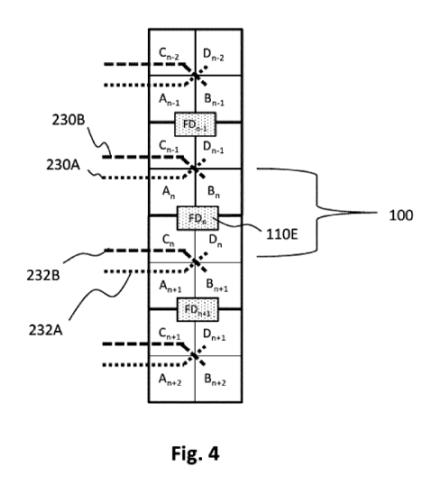
[0020] FIG. 4 illustrates a block diagram of a more detailed view a portion
of a pixel cell array
shown in FIG. 3.
[0021] FIGS. 5A and 5B illustrate schematic diagrams of a plurality of 4T
shared pixels in a
pixel array for providing differential digital double sampling according to an
exemplary
embodiment.
[0022] FIG. 6A illustrates a readout circuit of a CMOS image sensor for
providing differential
digital double sampling according to an exemplary embodiment.
[0023] FIG. 6B and 6C illustrates operational states of the readout circuit
shown in FIG. 6A
according to an exemplary embodiment.
[0024] FIG. 6D illustrates a schematic diagram of the readout circuit shown
in FIG. 6A
according to an exemplary embodiment.
[0025] FIGS. 7A and 7B illustrate timing diagrams of a pixel array of a
CMOS image sensor
for providing differential digital double sampling according to an exemplary
embodiment.
[0026] FIG. 8 illustrates a simulation of measured pixel output values of a
pixel array of a
CMOS image sensor for providing differential digital double sampling according
to an exemplary
embodiment.
7
CA 03035924 2019-03-06
WO 2018/046447 PCT/EP2017/072125
[0027] FIG. 9 illustrates a timing diagram of a vertical readout scheme for
a pixel array of a
CMOS image sensor for providing differential digital double sampling according
to an exemplary
embodiment.
[0028] FIG. 10 illustrates a block diagram of a CMOS image sensor for
providing differential
digital double sampling according to an exemplary embodiment.
DETAILED DESCRIPTION
[0029] Various aspects of the disclosed system and method are now described
with reference
to the drawings, wherein like reference numerals are used to refer to like
elements throughout. In
the following description, for purposes of explanation, numerous specific
details are set forth in
order to promote a thorough understanding of one or more aspects of the
disclosure. It may be
evident in some or all instances, however, that any aspects described below
can be practiced
without adopting the specific design details described below. In other
instances, well-known
structures and devices are shown in block diagram form in order to facilitate
description of one or
more aspects. The following presents a simplified summary of one or more
aspects of the
invention in order to provide a basic understanding thereof.
[0030] FIG. 2 illustrates a schematic diagram of an exemplary 4T shared
pixel CMOS image
sensor that can be implemented in connection with an exemplary embodiment. The
pixel 100
includes a similar configuration as the 4T pixel described above except that
it includes four sub-
pixels, i.e., photodiodes 110A, 110B, 110C and 110D (also shown as PDO-PD3)
that are each
driven by a respective transfer gate (shown as TGO-TG3). The transfer gates,
which are CMOS
transistors, are identified by reference numerals 112A, 112B, 112C and 112D.
As shown, each of
8
CA 03035924 2019-03-06
WO 2018/046447 PCT/EP2017/072125
the transfer gates 112A-112D shares a common readout circuit and is connected
to floating
diffusion point, 114, i.e., capacitor Cfd. As further shown, both transistor
116 (reset transistor) and
transistor 117 have drains connected to the voltage source ofthe pixel (i.e.,
VDD PIX). The source
of reset transistor 116 is connected to the floating diffusion point 114 and
the source of transistor
117 is connected to the drain of the select transistor 118. The source of
select transistor 118 is
connected to the column circuit 119.
[0031] As will be discussed in more detail below, each sub-pixel (i.e.,
each of photodiodes
PDO-PD3) can be read out separately by activating its corresponding transfer
gate. Thus, to read
out photodiode 110A, the transfer gate 112A is turned on/activated, then
photodiode 110B is read
out by activating transfer gate 112B, and so forth. In some instances,
multiple sub-pixels will be
read out at the same time as a single read operation by activating the
respective transfer gates
simultaneously. The specific operation and read out method will be described
in detail below with
respect to the timing diagram as an example. Moreover, it should be
appreciated that the
exemplary 4T 4 shared pixel shown in FIG. 2 provides one example of a pixel
for a pixel array
that can be implemented using the differential digital double sampling
technique described herein.
However, the inventive technique can also be implemented on other similar
types of pixel designs
and is not limited to the specific configuration shown in FIG. 2.
[0032] FIG. 3 illustrates a top-down view of a portion of a pixel cell
array configured to
perform differential digital double sampling according to an exemplary
embodiment. The pixel
array 200 includes a multitude of pixels described above. For example, as
shown in the middle of
the exemplary array 200, pixel 100 is shown as a solid dark square and
includes sub-pixels (i.e.,
photodiodes PDO-PD3) identified as photodiodes 110A-110D. As further shown, a
pixel including
9
CA 03035924 2019-03-06
WO 2018/046447 PCT/EP2017/072125
photodiodes 120A, 120B, 120C and 120D is shown in the array row above the row
of pixel 100
and another pixel including photodiodes 130A, 130B, 130C and 130D is shown in
the array row
below the row of pixel 100.
[0033] According to the exemplary embodiment, there are six columns of
subpixels in the
array with pairs of columns each having a respective pair of subpixels that
together form a pixel.
Moreover, the array 200 preferably comprises vertical shift registers that are
1125 lines deep, i.e.,
1125 rows in the array 200. Thus, in this embodiment, the platform for the
array is limited to 1125
rows times six columns or 6750 lines at maximum speed. Moreover, as will be
explained in detail
below, the differential digital double sampling is performed with one dark
level per two subpixels,
which facilitates reduction of consumed bandwidth compared with existing pixel
array readout
techniques.
[0034] As further shown, each of the photodiodes of pixel 100 are connected
to its respective
transfer gate as described above. Thus, photodiode 110A is connected to
transistor 112A,
photodiode 110B is connected to transistor 112B, photodiode 110C is connected
to transistor
112C, and photodiode 110D is connected to transistor 112D. Although pixel 100
is illustrated
with a solid line square, the array 200 provides a cross connection of pixels
such that sub-pixels
of adjacent pixels are readout concurrently to minimize bandwidth. Each
readout is illustrated
with dashed lines and boxes. Thus, the sub-pixels forming the grouping of sub-
pixels 210 is
readout first followed by the grouping of sub-pixels 220, as will become
readily apparent based on
the following disclosure. It should be appreciated that the readout scheme
shown in FIG. 3 is an
exemplary embodiment, but that the differential digital double sampling
technique described
herein can be implemented in other configurations without the cross-connection
design. For
CA 03035924 2019-03-06
WO 2018/046447 PCT/EP2017/072125
example, the inventive differential digital sampling technique could also be
implemented in pixel
configurations where the subpixels were addressed individually.
[0035] Thus, photodiode 110C (PD2) of pixel 100 is readout concurrently
when photodiode
120B (PD1) of the pixel in the row above is readout. Similarly, photodiode
110D (PD3) of pixel
100 is readout concurrently when photodiode 120A (PDO) of the pixel in the row
above is readout.
Moreover, when photodiode 110A (PDO) of pixel 100 is readout, photodiode 130D
(PD3) of the
pixel in the row below is also readout. Similarly, when photodiode 110B (PD1)
of pixel 100 is
readout, photodiode 130C (PD3) of the pixel in the row below is also readout.
[0036] As explained above with reference to FIG. 2, to readout a value of a
particular
photodiode, the respective transfer gate must be activated. In this instance,
transfer gate signals
are applied to pixels in adjacent rows, but not being part of the pixel, to
read out two values
concurrently. For example, as shown a transfer gate signal TG0/3 (i.e., signal
230A) is applied to
transistor 112A, such that the pixel 110A can be read out as shown above. As
further shown, this
transfer gate signal 230A is also applied to the transfer gate for photodiode
130D on the adjacent
row below the row of pixel 100. During the same clock cycle that the transfer
gate signal 230A is
activated, the control circuit also activates transfer gate signal 230B, which
activates the transfer
gates for photodiode 110B of pixel 100 and photodiode 130C (i.e., PD2) ofthe
pixel directly below
pixel 100. As shown, transfer gate signal 230A and transfer gate signal 230B
are in the same row
of the shift register.
[0037] Furthermore, during the next readout period, transfer gate signals
232A and 232B will
be applied in a similar manner. Transfer gate signals 232A activates the
transfer gates for
photodiode 110C of pixel 100 and photodiode 120B of the pixel directly above
pixel 100 in the
11
CA 03035924 2019-03-06
WO 2018/046447 PCT/EP2017/072125
array 200. Similarly, transfer gate signals 232B activates the transfer gates
for photodiode 110B
of pixel 100 and photodiode 120C of the pixel directly above pixel 100 in the
array 200. The
specific timing and operation of pixel readout will be described in detail
below with respect to the
timing diagram, the technical benefits of which will be readily apparent by
the reduction of
bandwidth requirements.
[0038] FIG. 4 illustrates a block diagram of a more detailed view a portion
of a pixel cell array
shown in FIG. 3. In particular, the column shown includes pixel 100 referenced
above that
includes sub-pixels A., 13,, C. and D. These sub-pixels correspond to sub-
pixels 110A-110D as
discussed above. Moreover, as described above, each 4T shared pixel includes a
floating diffusion
point, which is illustrated as FD. and denoted by 110E in the figure. As
further shown, a 4T pixel
in the preceding row is formed by sub-pixels Ami, Bn_i, Cn_i and Di (including
floating diffusion
point FD) and two sub-pixels C._2 and 1)2 are formed above this pixel.
Similarly, the row
following pixel includes a 4T pixel formed by sub-pixels A.+1, B.-pi, C.+1 and
D.+1 (including
floating diffusion point FD.+1) and two sub-pixels A.+2 and B.+2 are formed
below this pixel. For
purposes of this disclosure, the row for each pixel can be consider as rows n-
2, n-1, n, n+1 and
n+2.
[0039] As described above, each transfer gate is activated for two adjacent
sub-pixels in the
vertical direction (relative to the array) that are in different adjacent
pixel rows (e.g., in n-1 and n
rows or inn and n+1 rows). Thus, the transfer gates for sub-pixels C._i and B.
is first activated by
transfer gate signal 230B. Since these sub-pixels C._i and B. are in different
rows, i.e., different
pixels, the values can be readout during the same clock cycle. Next, a
transfer gate signal 230A is
applied to activate sub-pixels A. and D.4. As will be discussed in more detail
below, the readout
12
CA 03035924 2019-03-06
WO 2018/046447 PCT/EP2017/072125
of the n pixel row (i.e., pixel 100) is the double bright value of A. and B.
Since the value of B.
was already determined in response to activation by transfer gate signal 230B,
the pixel value of
A. can be determined by subtracting the value o f B. from double bright value
of A. and B., as well
as subtracting the dark value of the pixel). After the activation by the pair
of transfer gate signals
230A and 230B, the CMOS image sensor has performed a readout of sub-pixels A.,
B., Gi and
D.4. It should be appreciated that this readout corresponds to the dashed box
shown in FIG. 3 in
which sub-pixel 110A (i.e., A.), sub-pixel 110B (i.e., Be), sub-pixel 130C
(i.e., C.4), and sub-pixel
130D (i.e., D.4), are all readout during one clock cycle.
[0040] Referring back to FIG. 4, during the next cycle of readout, transfer
gate signals 232B
and 232A are applied to activate the corresponding pixels. In a similar manner
as described above,
the transfer gates for sub-pixels C. and B.+1 is first activated by transfer
gate signal 232B. Next,
transfer gate signal 232A is applied to activate sub-pixels A.+1 and D. The
readout of the n pixel
row (i.e., pixel 100) is the double bright value of G and D. Since the value
of C. was already
determined in response to activation by transfer gate signal 232B, the pixel
value of C. can be
determined by subtracting the value of D. and the dark value of the pixel from
the double bright
value of C. plus D. Accordingly, after the activation by the pair of transfer
gate signals 232A and
232B, the CMOS image sensor has performed a readout of sub-pixels C., D, A.+1
and B.+1.
[0041] FIGS. 5A and 5B illustrate schematic diagrams of a plurality of 4T
shared pixels in a
pixel array for providing differential digital double sampling according to an
exemplary
embodiment. As shown in FIG. 5A, the array includes a pair of adjacent rows,
i.e., 1st pixel row
n-1 and 2nd pixel row n, in the vertical direction of the array. It should be
appreciated that each
separate pixel in row n and n-1 includes the same 4T shared transistor circuit
configuration
13
CA 03035924 2019-03-06
WO 2018/046447 PCT/EP2017/072125
discussed above with respect to FIG. 2 and will not be repeated herein. As
shown, one transfer
gates signal 230A is applied to the transfer gate (TGO) of sub-pixel Cn_i and
to the transfer gate
(TG3) of sub-pixel B. Similarly, another transfer gates signal 230B is applied
to the transfer gate
(TG2) of sub-pixel A. and to the transfer gate (TG1) of sub-pixel
[0042] FIG. 5B illustrates the same pixel array circuit diagram and also
shows application of
additional transfer gates signal 232A and 232B, which are the same transfer
gate signals described
above. In both figures, the output of each pixel is connected to the column
circuit to provide
readouts as will be described in greater detail below. The timing of the
readout of the pixel array
is described as follows.
[0043] FIG. 6A illustrates a readout circuit of a CMOS image sensor for
providing differential
digital double sampling according to an exemplary embodiment. As shown, the
circuit includes
four capacitors 610A, 610B, 620A and 620B that are provided to store the video
level and the dark
level for the digital double sampling. In particular, two "bright" capacitors
(i.e., capacitors 620A
and 620B) are provided to sample the video level and two "dark" capacitors
(i.e., capacitors 610A
and 610B) are provided to sample the reference level. Thus, as shown,
capacitors 610A and 610B
are coupled to a capacitor reference voltage to readout a fixed value from the
reference voltage
while capacitors 620A and 620B are coupled to the bitline (i.e., a column
readout) of the pixel
array to sample the pixel voltages of the dark, bright and double bright
values of each pixel output
(i.e., the video level). The readout path is fully differential and the
connection of each capacitor
depends on the mode of operation as will be described in detail below.
[0044] At the end of column line 119, there are two switches, 621A and 621B
for selectively
connecting the output of the pixel array to storage capacitors 620A and 620B
to sample the dark,
14
CA 03035924 2019-03-06
WO 2018/046447 PCT/EP2017/072125
bright and double bright values, respectively, from the pixel array. Moreover,
the readout circuit
includes are two more switches, 611A and 611B for selectively connecting the
storage capacitors
610A and 610B to a reference voltage for the capacitors.
[0045] Each of the capacitors 620A, 620B, 610A and 610B is respectively
connected in
parallel to a reset switch 631A, 631B, 631C and 631D, in order to reset the
capacitors to a previous
value to GND. As will be discussed below, a reset signal RST CCAP is
periodically applied at
every count in the counter cycle during pixel sampling and readout. Moreover,
column selection
switches 641A-641D are respectively provided between the storage capacitors
and a bus bar (not
shown) that ultimately outputs the measured differential voltages to an AID
converter (also not
shown) and then to a buffer. Thus, the column selection switches 641A-641D are
controlled to
output stored signals from storage capacitors 610A, 610B, 620A and 620B to one
of the columns
at a time to the bus bar. Each of the pixels is activated at a given time by a
row decoder.
[0046] Advantageously, using this design, the sampling of the pixel output
voltage from the
pixel array is decoupled from the AID conversion. The decoupling enables high
speed readout of
the pixel output voltages by putting these two actions in parallel instead of
serial operation.
[0047] FIG. 6B and 6C illustrates operational states of the readout circuit
shown in FIG. 6A
according to an exemplary embodiment. As shown, the switches 621A and 641A as
well as
switches and 621B and 641B alternatively toggle between open and closed states
such that while
capacitor 620A is obtaining a readout value from the pixel array (e.g., FIG.
6B), the value in
capacitor 620B is being readout. Similar operation is also performed for
witches 611A and 641C
as well as 611B and 641D for the reference voltage. The details of circuit and
these operations are
explained as follows.
CA 03035924 2019-03-06
WO 2018/046447 PCT/EP2017/072125
[0048] In particular, FIG. 6D illustrates a schematic diagram of the
readout circuit shown in
FIG. 6A according to an exemplary embodiment. In general, the column readout
circuit is formed
from four column capacitors, i.e., capacitors 610A, 610B, 620A and 620B,
selectively coupled to
the pixel array by a plurality of switches. As noted above, storage capacitors
620A and 620B are
provided to sample the dark, bright and double bright values, respectively,
from the pixel array.
Moreover, the storage capacitors 610A and 610B are provided to sample a
reference voltage for
the capacitors.
[0049] According to the exemplary embodiment, the capacitors are configured
to decouple the
horizontal readout from the pixel array by receiving the sampled values on
bitline 119. In this
aspect, for each count, two capacitors are sampled and two capacitors are
readout in an alternating
manner. Thus, each of the switches is driven based on corresponding reset and
control signals.
As noted above, each of the capacitors is connected in parallel to a reset
switches 631A, 631B,
631C and 631D, respectively. During each count of operation a short pulse
(e.g., 49 nanoseconds)
is activated to reset the capacitors by closing the switch to force the ground
connection.
[0050] Furthermore, capacitors 620A and 620B are coupled to the bitline 119
by switches
621A and 621B. In the example of FIG. 6D, capacitor 620A is connected to the
bitline 119 since
switch 621A is closed. Thus, capacitor 620A is in a sampling mode, i.e., it is
sampling one of the
dark, bright and double bright values being output from the pixel array.
Alternatively, capacitor
620B is not currently connected to bitline 119 since switch 621B is open. In
the next count, a
control signal will close switch 621B and open switch 621A to reverse the
operations. As further
shown, column connection switches 641A and 641B connect capacitors 620A and
620B to the
downstream circuit, including the AID converter (not shown). In this example,
switch 641B is
16
CA 03035924 2019-03-06
WO 2018/046447 PCT/EP2017/072125
closed to connect capacitor 620B to the bus bar downstream, and, therefore,
being readout by the
circuitry. Column connection switches 641A and 641B are reversed in the next
count so that
capacitor 620A can be read out.
[0051] The switches connected to capacitors 610A and 610B operate in a
similar manner as
those switches discussed above. As shown, capacitors 610A and 610B are coupled
to the capacitor
reference voltage (i.e., REF1) by switches 611A and 611B. In the example
shown, capacitor 610A
is connected to the reference voltage since switch 611A is closed. Thus,
capacitor 610A is in a
sampling mode, i.e., it is sampling the reference voltage. Alternatively,
capacitor 610B is not
currently connected to reference voltage since switch 611B is open. In the
next count, a control
signal will close switch 611B and open switch 611A to reverse the operations.
As further shown,
column connection switches 641C and 641D connect capacitors 610A and 610B to
the downstream
circuit, including the A/D converter (not shown). In this example, switch 641D
is closed
connecting capacitor 610B to the bus bar downstream, and, therefore, being
readout by the
circuitry. These switches are reversed in the next count so that capacitor
610A can be read out.
[0052] In operation, the capacitors CB1 and CB2 (i.e., capacitors 620A and
620B)
alternatively sample values from pixel array (via bitline 119) and readout
values downstream to
the AID converter. Likewise, the capacitors CD1 and CD2 (i.e., capacitors 610A
and 610B)
alternatively sample values from the reference voltage and readout values
downstream to the AID
converter. Thus, a voltage difference between the sampled pixel values and the
sampled reference
value is continuously output from the column readout circuit to provide a
value of each sub-pixel,
including both the non-energized state and energized state for the digital
double sampling
17
CA 03035924 2019-03-06
WO 2018/046447 PCT/EP2017/072125
processing. The operation of the CMOS image sensor is explained in more detail
in the timing
diagram described as follows.
[0053] Specifically, FIG. 7A illustrates a timing diagram of a pixel array
of a CMOS image
sensor for providing differential digital double sampling according to an
exemplary embodiment.
As shown, the horizontal readout scheme is based on the counter, i.e., the 4k
SubCnt, which
provides a six count to perform each readout. In this regard, the counter
performs the count
operation in synchronization with clocks having a fixed period. In one
embodiment, the readout
is performed in accordance with the 1080p standard with each readout (i.e.,
each clock cycle) being
performed at 14.86 ps. In general, after each readout cycle, there are six
values that are obtained,
two dark values, two bright values, and two double bright values. After the
differential digital
double sampling technique is applied using these values, corrected digital
outputs of four pixels
can be obtained, which generates a 4k/UHD standard.
[0054] For purposes of illustration, the timing diagram is annotated in
accordance with the
sub-pixels shown in FIG. 4 and discussed above. As shown, at a first count
value, a reset signal
Rstl is applied to row n-1, and more particularly, to reset floating diffusion
point fd._i . Preferably,
the reset signals have a width of 22 clks at 222 MHz or 99 nanoseconds. During
this same count,
a select signal Sell is applied to row n-1, i.e., R.4. Preferably, the select
signals have a width of
210 clks at 222 MHz or 943 nanoseconds. Similarly, at a second count value, a
reset signal Rst2
is applied to row n, i.e., to floating diffusion point fd., and a select
signal 5e12 is applied to row n,
i.e., to R. Thus, it should be appreciated that in accordance with the DDS
filtering technique,
each of rows n-1 and n have been reset such that the digital data Drst (i.e.,
dark values) for each
18
CA 03035924 2019-03-06
WO 2018/046447 PCT/EP2017/072125
pixel can obtained. This is shown in the readout row (i.e., "READ") in which
the dark values R._
1 and R. are read out from the pixel array during counts 2 and 3 of the clock
cycle.
[0055] In general, the timing diagram illustrates that the capacitors are
reset by RST CCAP
value at the top of each count and the control signal SW _B for capacitors
620A and 620B and the
control signal SW D for capacitors 610A and 610B are continuously applied
(i.e., the switches a
repeatedly toggled from an open state to a closed state as described above) to
sample the date on
the bitline as should be understood to those skilled in the art. The resetting
and sampling of these
capacitors will not be described for each separate count in the cycle.
[0056] Once the dark values R.4 and R. are sampled at counts 1 and 2 and
readout at counts
2 and 3, the timing continues to count 3 of the cycle. As shown, a transfer
gate TG1/2 is applied to
activate the corresponding sub-pixel in rows n-1 and n. For example, this
transfer gate signal TG1/2
corresponds to signal 230B described above and activates sub-pixels C._i and
B. Thus, when
select signal Sell is applied again to row n-1, sub-pixel C.4 can be readout
as further shown during
count 4. Similarly, when select signal 5e12 is applied again to row n, sub-
pixel B. can be readout
as further shown during count 5. Preferably, the transfer gate signals have a
width of 320 clks at
222 MHz or 1437 nanoseconds. It is noted that the bright value read out (e.g.,
sub-pixel C.4) will
also include the correspond dark value (e.g., dark value R.4). Thus, as
further described herein,
the bright value is calculated by subtracting the measured dark value R._i
from the measured bright
value C.4, and so forth.
[0057] Furthermore, during count 5, a transfer gate TGon is applied to
activate the
corresponding sub-pixels in row n and n-1. This transfer gate signal TGon
corresponds to signal
230A described above and activates sub-pixels D.4 and A. Thus, when select
signal Sell is
19
CA 03035924 2019-03-06
WO 2018/046447 PCT/EP2017/072125
applied again to row n-1, a double bright value of both sub-pixel C.4 and D._i
can be readout as
further shown during count 6. Similarly, when select signal 5e12 is applied
again to row n, a double
bright value of sub-pixel B. and sub-pixel A. can be readout as further shown
during count 1 of
the next clock cycle. Accordingly, during this counter cycle, the readout
circuit has sampled values
from sub-pixels C.4 and B. and double bright values from sub-pixels C._i and
Di and from sub-
pixels A. and B. as well as the corresponding dark values Rii_i and R. As will
be described below,
the values for sub-pixels Di can be determined by removing the value of C._i
from the double
bright value and the dark value R._i and so forth. Similarly, the values for
sub-pixels A. can be
determined by removing the value of B. from the double bright value as well as
the dark value R.
[0058] After the six count of the clock cycle, the shift register clock
shifts to the next row in
the pixel array. FIG. 7B illustrates a timing diagram of the control signals
in the next row in the
array. The same operations are performed as that described above for the
timing diagram of FIG.
7A and will not be repeated herein.
[0059] FIG. 8 illustrates a simulation of measured pixel output values of a
pixel array of a
CMOS image sensor for providing differential digital double sampling according
to an exemplary
embodiment. As shown, the initial dark values (i.e., Dark._i or Di and Dark.
or D.) are measured
at a first value of slightly below 283d. Next, measured values of sub-pixels
C._i or Bare measured
at approximately 680d. Furthermore, a double-bright value for Ci and Di is
measured at slightly
over the 940d value. Thus, applying the digital double sampling method
described herein, the
values of sub-pixels C._i and B. can be calculated by subtracting the dark
values Dark.4 (i.e., D._
1) and Dark. (i.e., D.) , respectively. Moreover, the value of sub-pixel Di
can be determined by
subtracting form the measured value the value of sub-pixel C._i and dark value
Dark.4 (i.e., D.4).
CA 03035924 2019-03-06
WO 2018/046447 PCT/EP2017/072125
It should be appreciated that this simulation is based on the current cross-
connection pixel readout
scheme described above and shown in the figures, such as FIG. 4, for example.
In alternative
embodiments, if the cross-connection was not used for the technique, the order
of pixel readout
could be, for example, dark, bright, double bright, dark, bright, double
bright (instead of dark,
dark, bright, bright, double bright, double bright).
[0060] FIG. 9 illustrates a timing diagram of a vertical readout scheme for
a pixel array of a
CMOS image sensor for providing differential digital double sampling according
to an exemplary
embodiment. As noted above, the pixel array described herein (i.e., pixel
array 200 shown in FIG.
3) preferably comprises vertical shift registers that are 1125 lines deep,
i.e., 1125 rows in the array
200. Thus, the client VCiosop is shown as having counts 1 through 1125. Each
of reset signals
RST1 and RST, select signals SEL1 and SEL 2, and transfer gate activation
signals TG0/3 and
TG1/2 are shown as cycling through in rows in response to control signals
received from a row
decoder as would be understood to one skilled in the art. It should be
appreciated that there are
corresponding reset, select and transfer gate activation signals for each row
in the pixel array 200.
Thus, the rows are cycled through to be sampled as described using the timing
operation described
herein.
[0061] Finally, FIG. 10 illustrates a block diagram of a CMOS image sensor
for providing
differential digital double sampling according to an exemplary embodiment. As
shown, the CMOS
image sensor 900 includes a pixel array 910, which can be, for example, pixel
array 200 described
herein that includes a multitude of 4T share pixel configurations.
Furthermore, the output of the
pixel array 910 is fed to an analog readout path and AID converter 920, which
is provided for
processing the analog output voltages from the pixel array 910 to convert
analog pixel signals into
21
CA 03035924 2019-03-06
WO 2018/046447 PCT/EP2017/072125
digital signals. It should be understood that the analog readout path and AID
converter 920
includes the readout circuit shown in FIGS. 6A-6D and AID converters for
converting the
measured analog signals to digital signals as is known to those skilled in the
art.
[0062] As further shown, a latch array unit (or line buffer) 930 is
provided for storing the
digital signals outputted from the analog readout path and A/D converter 920.
It should be
appreciated that the line buffer 930 can include multiple lines depending on
the readout order of
the pixels ofpixel array 910. Moreover, a control unit 950 is provided for
providing control signals
used in controlling the aforementioned units and outputting data to the
outside (e.g., a display unit)
through an interface. For example, the control unit 950 in conjunction with
row decoder 940
(collectively, a pixel sampler) can generate the activating signals described
above with respect to
FIGS. 7A and 7B. Moreover, in one embodiment, the control unit 950 can also
generate the
control signals to open and close the switches of the capacitor readout.
[0063] In addition, the data signals can be fed from the latch array unit
830 to the control unit
950. According to an exemplary embodiment, the bright values of each
photodiode can be
calculated by the control unit 950, i.e., a pixel output calculator, by
subtracting the respective dark
value for that pixel from the sampled bright value. For example, the sampled
bright value B. as
shown in FIG. 7A can be calculated by subtracting the dark value R. from the
combined output
value of B. plus R. Similarly, the bright value A. can be calculated by
subtracting the dark value
R. and the sampled bright value B. from the combined output value of bright
values A. and B.
plus the dark value R. These calculations can be performed in software,
hardware or a
combination thereof as would be appreciated to one skilled in the art.
22
CA 03035924 2019-03-06
WO 2018/046447 PCT/EP2017/072125
[0064] The control unit 950 can includes one or more processors and one or
more modules for
executed the control algorithms described herein. The modules may be software
modules running
in the processor, or resident/stored in memory, one or more hardware modules
coupled to the
processor, or some combination thereof Examples of processors include
microprocessors,
microcontrollers, digital signal processors (DSPs), field programmable gate
arrays (FPGAs),
programmable logic devices (PLDs), state machines, gated logic, discrete
hardware circuits, and
other suitable hardware configured to perform the various functionality
described throughout this
disclosure. One or more processors in the processing system may execute
software. Software
shall be construed broadly to mean instructions, instruction sets, code, code
segments, program
code, programs, subprograms, software modules, applications, software
applications, software
packages, routines, subroutines, objects, executables, threads of execution,
procedures, functions,
etc., whether referred to as software, firmware, middleware, microcode,
hardware description
language, or otherwise.
[0065] Furthermore, the control unit 950 is coupled to a row decoder 940,
which can be
considered a pixel sampler of the pixel array, for example, that is configured
to output the signals
for selecting the rows in the pixel array 910 based on a control signal
transmitted from the control
unit 950.
[0066] Preferably the analog readout path and AID converter 920 includes
comparators as
many as the number of columns of the pixel array 910 as described above. Each
of the comparators
serves a role of converting an analog pixel value of a column in which it is
located into a digital
signal. The digital signal is stored in the latch array unit 930 including
latches as many as the
number of the columns of the pixel array 910. The digital signals stored in
the latch array unit 930
23
CA 03035924 2019-03-06
WO 2018/046447 PCT/EP2017/072125
are subjected to an image processing by the control unit 950 and then,
sequentially outputted
through output pins of the image sensor in the image processed order. Thus,
the control unit 950
is configured to output data to generate image data to be displayed on a
screen of an electronic
device as would be appreciated to one skilled in the art.
[0067] According to the disclosure herein, the exemplary method and sensor
provide for an
efficient readout of pixel values from a pixel array that reduces the required
output bandwidth and
enables digital double sampling through the whole analog chain of the pixel
array. Moreover,
using the disclosed technique, effects like Black sun and fluctuating analog
disturbances are
avoided and suppressed.
[0068] Advantageously, during sampling of the dark values, when the imager
sensor receives
no light during the first sample, the dark value holds the kTC, and the second
and third samples
also contain kTC, since no photo charge is added. Thus, all pixels hold
readnoise only, and the
kTC is suppressed.
[0069] Moreover, the CMOS image sensor and method described herein avoids
the need for
optical Black lines with a digital clamp. In general, optical black is very
difficult to make since
the broadcast lightning is very bright and cannot be shielded 100%. This
technical limitation
results in visible artifacts. The disclosed CMOS image sensor and method
prevents and/or limits
such artifacts. A clamp always generates some low frequency noise, which is
very disturbing.
Moreover, the residue error in a lineclamp results in vertical lines in the
image. Thus, the CMOS
image sensor avoids the need for optical Black lines with a digital clamp.
[0070] It should be appreciated that in the examples above, all switching
signals are assumed
to be positive logic signals, i.e. a high level, or "1" results in closing the
switch. It is, however,
24
CA 03035924 2019-03-06
WO 2018/046447 PCT/EP2017/072125
also possible to use an inverted logic, or to use both, positive and negative,
logic in a mixed
manner. Moreover, the disclosed CMOS image sensor and method reduces the noise
created in
the digital double sampling stage, as described above, provides an increased
speed of the overall
readout circuit. In one aspect, the increase in the speed of the readout
circuit allows for an increase
in the number of pixels in a matrix, which is a key feature for high
definition imaging.
[0071] While aspects have been described in conjunction with the example
implementations
outlined above, various alternatives, modifications, variations, improvements,
and/or substantial
equivalents, whether known or that are or may be presently unforeseen, may
become apparent to
those having at least ordinary skill in the art. Accordingly, the example
implementations of the
invention, as set forth above, are intended to be illustrative, not limiting.
Various changes may be
made without departing from the spirit and scope of the aspects. Therefore,
the aspects are
intended to embrace all known or later-developed alternatives, modifications,
variations,
improvements, and/or substantial equivalents.
[0072] Thus, the claims are not intended to be limited to the aspects shown
herein, but is to be
accorded the full scope consistent with the language claims, wherein reference
to an element in
the singular is not intended to mean "one and only one" unless specifically so
stated, but rather
"one or more." Unless specifically stated otherwise, the term "some" refers to
one or more. All
structural and functional equivalents to the elements of the various aspects
described throughout
this disclosure that are known or later come to be known to those of ordinary
skill in the art are
expressly incorporated herein by reference and are intended to be encompassed
by the claims.
Moreover, nothing disclosed herein is intended to be dedicated to the public
regardless of whether
CA 03035924 2019-03-06
WO 2018/046447 PCT/EP2017/072125
such disclosure is explicitly recited in the claims. No claim element is to be
construed as a means
plus function unless the element is expressly recited using the phrase "means
for."
26