Note: Descriptions are shown in the official language in which they were submitted.
CA 03036478 2019-03-11
WO 2018/052397
PCMJS2016/051464
Buffer Layer To Prevent Etching By Photoresist Developer
TECHNICAL FIELD
The present disclosure relates to buffer layers for preventing etching by a
photoresist developer.
BACKGROUND
Quantum computing is a relatively new computing method that takes advantage
of quantum effects, such as superposition of basis states and entanglement to
perform
certain computations more efficiently than a classical digital computer. In
contrast to a
digital computer, which stores and manipulates information in the form of bits
(e.g., a
(:) "1" or "0"), quantum computing systems can manipulate information using
qubits. A
qubit can refer to a quantum device that enables the superposition of multiple
states
(e.g., data in both the -0" and -1" state) and/or to the superposition of
data, itself, in the
multiple states. In accordance with conventional terminology, the
superposition of a
"0" and "1" state in a quantum system may be represented, e.g., as ci0> +
1311>. The "0"
and "1- states of a digital computer are analogous to the 10> and 1i> basis
states,
respectively of a qubit. The value Ict2 represents the probability that a
qubit is in 0>
state, whereas the value 11312 represents the probability that a qubit is in
the 11> basis
state.
SUMMARY
In general, in a first aspect, the subject matter of the present disclosure
may be
embodied in methods of fabricating a quantum circuit device, the methods
including:
providing a device having a first layer and a second layer in contact with a
surface of
the first layer, in which the second layer includes a first superconductor
material that
exhibits superconducting properties at or below a corresponding
superconducting
critical temperature; forming a buffer material on a surface of the second
layer to form
an etch buffer layer, in which an etch rate selectivity of the buffer material
relative to
the second layer upon exposure to a photoresist developer is such that the
underlying
second layer is not etched during exposure of the buffer layer to the
photoresist
1
CA 03036478 2019-03-11
WO 2018/052397
PCT/US2016/051464
developer; depositing and removing a selected portion of a resist layer to
uncover a first
portion of the etch buffer layer, wherein removing the selected portion of the
resist
layer comprises applying the photoresist developer to the selected portion of
the resist
layer..
Implementations of the methods may include one or more of the following
features. For example, in some implementations, the etch rate selectivity of
the buffer
material relative to the second layer upon exposure to the photoresist
developer is less
than 1:2.
In some implementations, the first superconductor material of the second layer
is aluminum.
In some implementations, the buffer material includes a polymer. The polymer
may include polymethylmethacrylate (PMMA).
In some implementations, the methods further include removing the uncovered
first portion of the etch buffer layer to uncover a first portion of the
second layer.
Removing the uncovered first portion of the etch buffer layer may include
subjecting
the uncovered first portion of the etch buffer layer to a dry etch. The dry
etch includes
an 02 plasma. The methods may further include etching the uncovered first
portion of
the second layer. The etched second layer may form part of the quantum circuit
device,
in which the quantum device includes a qubit, a qubit measurement resonator, a
superconducting quantum interference device, a superconducting coupler, or a
superconducting co-planar waveguide. The methods may further include removing,
subsequent to etching the uncovered first portion of the second layer, a
remaining
portion of the resist layer and the etch buffer layer. The methods may further
include
forming a dielectric material or a second superconductor material, which
exhibits
superconducting properties at or below a corresponding superconducting
temperature,
on the uncovered first portion of the second layer. The second layer and the
dielectric
material or the second layer and the second superconductor material may form
part of
the quantum circuit device. The quantum circuit device may include a parallel
plate
capacitor, a microstrip resonator, or a transmission line. The methods may
further
include removing, subsequent to depositing the dielectric material or the
second
superconductor material, a remaining portion of the resist layer and the etch
buffer
layer.
2
In some implementations, the first layer includes a substrate. The substrate
may include a
silicon wafer or a sapphire wafer.
Implementations may include one or more of the following advantages. For
example, in
some implementations, the buffer material prevents developer from attacking
underlying
material, such as aluminum, thus preventing removal or damage of the
underlying material.
Moreover, as a result, in some implementations, it is not necessary to use
weaker developer
solutions, which may require longer development times. Alternatively, stronger
and faster
developer solutions may be used without concern that the material underlying
the buffer layer
will be attacked. Additionally, in some implementations, the buffer material
itself etches much
faster than photoresist under certain etching methods, such as 02 ashing, such
that the buffer
material may be removed without concern that the photoresist regions defining
various aspects of
the device to be fabricated will be damaged.
For the purposes of this disclosure, a superconductor (alternatively,
superconducting)
material may be understood as a material that exhibits superconducting
properties at or below a
superconducting critical temperature. Examples of superconductor material
include, but are not
limited to, aluminum (superconducting critical temperature of, e.g., 1.2
kelvin), niobium
(superconducting critical temperature of, e.g., 9.3 kelvin) and titanium
nitride (superconducting
critical temperature of, e.g., 5.6 kelvin).
According to an aspect, there is provided a method of fabricating a quantum
circuit
device, the method comprising: providing a device having a first layer and a
second layer in
contact with a surface of the first layer, wherein the second layer comprises
a first
superconductor material that exhibits superconducting properties at or below a
corresponding
superconducting critical temperature; forming a buffer material on a surface
of the second layer
to form an etch buffer layer, wherein an etch rate selectivity of the buffer
material relative to the
second layer upon exposure to a photoresist developer is such that the
underlying second layer is
not etched during exposure of the buffer layer to the photoresist developer;
depositing and
removing a selected portion of a resist layer to uncover a first portion of
the etch buffer layer,
wherein removing the selected portion of the resist layer comprises applying
the photoresist
developer to the selected portion of the resist layer; removing the uncovered
first portion of the
etch buffer layer to uncover a first portion of the second layer; and forming
a dielectric material
or a second superconductor material, which exhibits superconducting properties
at or below a
3
Date Recue/Date Received 2021-02-01
corresponding superconducting temperature, on the uncovered first portion of
the second layer,
wherein the second layer and the dielectric material or the second layer and
the second
superconductor material form part of the quantum circuit device, the quantum
circuit device
comprises a parallel plate capacitor, a microstrip resonator, or a
transmission line.
The details of one or more implementations are set forth in the accompanying
drawings
and the description below. Other features and advantages will be apparent from
the description,
the drawings, and the claims.
BRIEF DESCRIPTION OF THE DRAWINGS
FIGS. 1A-1C are schematics that illustrate cross-section views of an example
of a device
affected by developer damage to an aluminum film.
FIG. 2 is a photograph that illustrates a top view of an example of a device
affected by a
developer that has been diluted.
FIGS. 3A-3G are schematics illustrating an example of a process that utilizes
a buffer
layer to protect an underlying aluminum layer from etching by a developer
solution.
3a
Date Recue/Date Received 2021-02-01
CA 03036478 2019-03-11
WO 2018/052397
PCT/US2016/051464
DETAILED DESCRIPTION
Quantum computing entails coherently processing quantum information stored
in the quantum bits (qubits) of a quantum computer. In certain types of
quantum
computing processors, such as quantum annealers, the qubits of the quantum
processor
are coupled together in a controllable manner such that the quantum state of
each qubit
affects the corresponding quantum states of the other qubits to which it is
coupled.
Superconducting quantum computing is a promising implementation of quantum
computing technology in which quantum circuit elements are formed, in part,
from
superconductor materials. Superconducting quantum computers are typically
multilevel
.. systems, in which only the first two levels are used as the computational
basis. In
certain implementations, quantum circuit elements, such as qubits, are
operated at very
low temperatures so that superconductivity can be achieved and so that thermal
fluctuations do not cause transitions between energy levels. Additionally, it
may be
preferable that the quantum circuit elements are operated with low energy loss
and
dissipation (e.g., the quantum circuit elements exhibit a high quality factor.
Q). Low
energy loss and dissipation may help to avoid, e.g., quantum decoherence.
An example of a superconductor material that can be used in the formation of
quantum circuit elements is aluminum. Aluminum may be used in combination with
a
dielectric to establish Josephson junctions, which are a common component of
quantum
circuit elements. Examples of quantum circuit elements that may be formed with
aluminum include circuit elements such as superconducting co-planar
waveguides,
quantum LC oscillators, qubits (e.g., flux qubits or charge qubits),
superconducting
quantum interference devices (SQUIDs) (e.g., RF-SQUID or DC-SQUID), inductors,
capacitors, transmission lines, ground planes, among others.
Aluminum may also be used in the formation of superconducting classical
circuit elements that are interoperable with superconducting quantum circuit
elements
as well as other classical circuit elements based on complementary metal oxide
semiconductor (CMOS) circuity. Examples of classical circuit elements that may
be
formed with aluminum include rapid single flux quantum (RSFQ) devices,
reciprocal
quantum logic (RQL) devices and ERSFQ devices, which are an energy-efficient
version of RSFQ that does not use bias resistors. Other classical circuit
elements may
be formed with aluminum as well. The classical circuit elements may be
configured to
4
CA 03036478 2019-03-11
WO 2018/052397
PCT/US2016/051464
collectively carry out instructions of a computer program by performing basic
arithmetical, logical, and/or input/output operations on data, in which the
data is
represented in analog or digital form.
Processing with aluminum may, however, lead to various complications that
degrade the performance of the quantum circuit elements (as well as the
performance of
classical circuit elements). In particular, aluminum on semiconductor
substrates may be
highly susceptible to etching by photoresist developers that are used to
remove soluble
photoresist after exposure to light. This is understood to be primarily a
result of the
galvanic corrosion effect. For instance, in some cases, a 100 nm film of
aluminum can
be completely etched away if exposed to a common developer (e.g., AZ 300 M1F
from
AZ Electronic Materials) during a standard 60 second photoresist development
step. In
other cases, the developer may not etch away the entire aluminum film, but can
still
lead to significant roughening of the aluminum surface. This roughening may
increase
the surface loss associated with the aluminum film, which, in turn, may reduce
the
.. quality factor, Q, of a circuit element of which the aluminum film is a
component. For
example, in some implementations, the quality factor of a device using an
aluminum
surface roughened by developer may be reduced by a factor of two or more
(e.g., from
a Q of 3*106 to a Q of 1.3*106).
While the examples below are described in the context of aluminum as the
.. material that exhibits superconducting properties below a certain
temperature, the
processes described below can be applied to a superconducting material that
may be
susceptible to the galvanic corrosion effects to a degree that causes
unacceptable levels
of removal without the presence of a buffer material.
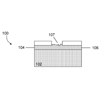
FIGS. 1A-1C are schematics that illustrate cross-section views of an example
of
a device 100 affected by developer damage to an aluminum film. As shown in FIG
la,
the device 100 initially includes a silicon substrate 102 on which is formed
an
aluminum layer 104. A layer of photoresist 106 may be provided on the top
surface of
the aluminum layer 104. A portion of the photoresist layer 106 may be exposed
to. e.g.,
ultraviolet (UV) light 101, such that the exposed portion 103 is now soluble
when a
developer is applied to the photoresist. The other portions 105 of the
photoresist layer
106 that have not been exposed to the UV light remain insoluble when coming
into
contact with the developer. The foregoing is an example of a positive type
resist.
5
CA 03036478 2019-03-11
WO 2018/052397
PCT/US2016/051464
Negative type resists may be used instead, in which the portion of the
photoresist that is
exposed to UV light becomes insoluble in developer, whereas the unexposed
portions
remain soluble in developer.
FIG 1B shows a first type of damage that can occur when the developer is
applied to the photoresist after the exposure step. In this image, the exposed
portion of
photoresist may be removed, but the developer continues to attack the
underlying
aluminum causing substantial roughness 107 in surface of the aluminum. As
explained
herein, the increased roughness may lead to a reduction in quality factor of
the quantum
circuit elements to be formed.
FIG IC shows a second type of damage that can occur when the developer is
applied to the photoresist after the exposure step. Again, the exposed portion
of
photoresist may be removed, but the developer completely etches away the
underlying
aluminum film. Indeed, the etch effect of the developer may be so severe that
portions
109 of the aluminum film are etched underneath the regions of photoresist that
have not
been removed by the developer.
Though using a weaker developer (e.g., a diluted developer) may, in some
cases, reduce the level of aluminum etching, this approach can substantially
increase
the time necessary to develop a photoresist layer. Moreover, diluting the
developer
renders removing all of the undesired photoresist more difficult. FIG 2 is a
photograph
that illustrates a top view of an example of a device affected by a developer
that has
been diluted. Three separate areas are evident in the photograph: a first
region 202
where UV exposed photoresist has been removed entirely by a diluted developer
to
reveal an underlying aluminum layer, a second region 204 where unexposed
resist
remains covering the underlying aluminum layer, and a third region 206 where
UV
exposed resist has not been cleared by the weakened developer. In some
implementations, the uncleared resist, such as the resist in region 206,
remains
regardless of how long the development time is, thus destroying the usability
of the
wafer.
The present disclosure relates to adding a buffer layer to the fabrication
process
10 prevent the developer attack/etching of films, such as aluminum. Using
aluminum as
an example type of film to be protected, the buffer layer has a developer etch
rate
selectivity that may be much lower relative to aluminum and may be positioned
6
CA 03036478 2019-03-11
WO 2018/052397
PCT/US2016/051464
between the aluminum film and an overlying photoresist layer during the
fabrication
process. Accordingly, once the developer removes the undesired photoresist,
only the
buffer layer, and not the aluminum layer, may be exposed to the developer
solution.
The buffer layer thus serves to protect the underlying aluminum layer.
Additionally,
given the low etch rate selectivity of the buffer layer in the presence of the
developer,
the buffer layer is not significantly etched. After performing
photolithography and
development, the exposed portion of the buffer layer may be removed to allow
for
deposition of further materials onto the underlying aluminum layer or to allow
for
removal of the underlying aluminum layer.
lt) FIGS. 3A-3F are schematics illustrating an example of a process that
utilizes a
buffer layer to protect an underlying aluminum layer from etching by a
developer
solution. First, as shown in FIG 3A, a device 300 is provided, in which the
device 300
includes a substrate 302 on which a thin film 304 of aluminum may be formed.
In the
present example, the aluminum film has a thickness of 100 nm, though other
thicknesses may be used as well. The substrate 302 may include, e.g., a
silicon or
sapphire wafer. Next, as shown in FIG 3B, a buffer layer 306 may be formed on
the top
surface of the aluminum layer 304. The buffer layer 306 includes a material
that may be
highly resistant to etching by common photoresist developers. For example, the
buffer
layer 306 may include an insulating electric polymer film, such as
.. polymethylmethacrylate (PMMA). An etch rate selectivity of the buffer
material
relative to aluminum upon exposure to a photoresist developer may be, e.g.,
less than
1:2, less than 1:3, less than 1:4, less than 1:5, less than 1:6, less than
1:10, less than
1:20, or less than 1:40. The buffer material may have other values for etch
rate
selectivity relative to aluminum in the presence of photoresist developer.
More
generally, the ratio may be such that the underlying aluminum is not etched
during
exposure of the buffer layer to the photoresist developer. As used herein, a
superconductor is not etched during exposure if superconductor is not removed
and the
surface of superconductor is not roughened to the point that the roughening
affects the
qualitative performance of the circuit for given performance requirements.
The buffer layer 306 may be deposited on the top surface of the aluminum layer
304 in liquid form using, e.g., a spin coater. As an example process, PMMA may
be
deposited on the aluminum film in liquid form and then spin coated at 8 krpm.
7
CA 03036478 2019-03-11
WO 2018/052397
PCT/US2016/051464
Following spinning, the device 100 then may be post-baked at 200 C for about
2 min
on a hot plate to provide a PMMA film that is several nanometers thick. Other
spin-
coating speeds and post-bake times may be used to achieve different
thicknesses for the
buffer layer 306.
Following deposition of the buffer layer 306, a photoresist layer 308 then may
be formed on the surface of the buffer layer 306, as also shown in FIG 3B. At
least a
portion 301 of the photoresist layer 308 then may be exposed to light 311
(e.g., UV or
DUV), causing a chemical change in the exposed resist such that the exposed
resist
becomes either soluble to photoresist developer or insoluble to photoresist
developer.
A developer then may be applied to the top surface of the device 100
containing
the photoresist layer 308 that has been exposed to light. For positive-type
photoresist,
the developer removes the photoresist in the region 301 that absorbed the
incident light,
while leaving the unexposed photoresist 303 remaining on the surface of the
buffer
layer 306 as shown in FIG 3C. For negative-type photoresist, the developer
removes
the portions of photoresist outside of the region 301, while leaving the
region 301 in
place on the buffer layer 306. The portion 305 of the buffer layer 306 that
comes into
contact with the developer solution during this step is not etched (or is not
substantially
etched). Rather, as shown in FIG 3C, the buffer layer 306, including the
region 305 that
comes into contact with the developer solution, serves as a barrier preventing
the
developer from reaching the underlying aluminum layer 304, and thus protecting
the
aluminum 304 from being etched.
The portion 305 of the buffer layer 306 that is bare/uncovered due to the
removal of photoresist then may be itself removed as shown in FIG 3D. In the
present
example, the buffer layer 306 includes PMMA and may be removed using 02 ashing
to
expose/uncover a region 307 of the underlying aluminum layer 304. In 02
ashing,
monatomic oxygen plasma is created by exposing oxygen gas at a low pressure to
high
power radio waves. The reactive oxygen then combines with the PMMA to form
ash,
which is removed with a vacuum pump. Although 02 ashing also removes
photoresist,
PMMA has a much higher etch rate selectivity compared to photoresist. For
example,
PMMA may have an etch rate selectivity for 02 ashing relative to photoresist
of greater
than 3:1. Accordingly, 02 ashing may be an effective technique for removing
the
PMMA buffer layer 306 without substantially removing the patterned photoresist
layer.
8
CA 03036478 2019-03-11
WO 2018/052397
PCT/US2016/051464
Other techniques for removing the buffer layer 306 may be used as well. The
etch
selectivity of a technique for removing the buffer layer 306 should be high
enough that
the patterned photoresist layer 308 is not removed or substantially degraded
during etch
of the buffer layer 306.
Following the removal of the portion 305 of the buffer layer 306, further
processing of the device 100 may include etching and/or material deposition.
For
example, in some implementations, the patterned photoresist/buffer layers may
define a
bare/uncovered region 307 of the aluminum layer 304 for etching. Etching of
the region
307 of the aluminum layer 304 may continue until the layer beneath the
aluminum film
304 (e.g., the substrate 302) is reached. For instance, a wet etchant, such as
etchants
available from Transene Company, Inc. may be used to remove the aluminum. In
some
implementations, the layer (e.g., substrate 302) beneath the aluminum film 304
also
may be etched using the film 304 as a mask. For example, as shown in FIG 3E, a
portion 309 of the substrate 302 may be etched following removal of the
aluminum
.. region 307. In some implementations, the entirety of the buffer layer 306
and the
photoresist layer 308 are removed after etching the region 307 of aluminum
film 304.
The photoresist may be removed using, for example, a solvent (e.g., acetone or
dimethyl sulfoxide) or photostripper (e.g., AZ 100 remover). The buffer layer
306
may be removed using 02 as detailed herein. In some implementations, the
remaining
-- photoresist layer 308 is removed before etching the layer 304.
Alternatively, or in addition to the etch process steps, material may be added
to
the device 100 following removal of the portion 305 of the buffer layer 306.
For
example, in some implementations, a layer of superconductor material (e.g.,
aluminum,
niobium or titanium nitride) may be deposited on the uncovered region 307 of
the
aluminum layer 304 and on the photoresist/buffer layer stack. Portions of the
deposited
superconductor on the photoresist/buffer layers 306/308 may then be removed
using,
e.g., a lift-off process. A remaining portion 310 of superconductor material,
having a
width defined by the now-removed photoresist/buffer layers 306/308 remains on
the
surface of aluminum layer 304, as shown in FIG 3F. Alternatively or in
addition, in
-- some implementations, a dielectric material (e.g., an electrically
insulating material)
may be deposited on the uncovered region 307 of the aluminum layer 304 and on
the
photoresist/buffer layer stack. The dielectric material may include, e.g.,
amorphous or
9
CA 03036478 2019-03-11
WO 2018/052397
PCT/US2016/051464
poly-crystalline silicon or silicon dioxide. Other materials may be deposited
as well.
Alternatively, in some implementations, material may be added to the device
100
following the removal of the portion 307 of the aluminum layer 304. For
example, a
superconductor, dielectric or metal may be deposited on an uncovered portion
of the
substrate 302 following etching of aluminum, but prior to the removal of the
photoresist/buffer stack. Again, a lift-off process may be used to remove the
portions of
the material arranged on the photoresist/buffer layer. Alternatively, the
photoresist and
buffer layer may be removed prior to deposition of the new layer of material.
For
example, FIG. 3G is a schematic that illustrates an example of device 300, in
which a
conformal dielectric 312, such as silicon dioxide or amorphous silicon, may be
deposited (using, e.g., chemical vapor deposition) on a surface of the
aluminum layer
304, after the aluminum has been etched to expose a portion of the underlying
substrate
302.
Though the present disclosure describes examples of a buffer layer for
protecting aluminum films against etching by a developer solution, a buffer
layer may
also be used to protect other films/materials that are susceptible to
substantial etching
by a developer solution (e.g., zinc or other materials susceptible to galvanic
corrosion).
As explained herein, the aluminum layer (or other layer) that is protected
from
etching by the developer solution by the buffer material may be used as part
of a
quantum circuit element or a classical circuit element. Additional layers and
components can be formed, added and/or etched by repeating one or more of the
process steps described herein with respect to FIGS. 3A-3G one or more times.
Processes described herein may entail the deposition of one or more materials,
such as superconductors, dielectrics and/or metals. Depending on the selected
material,
these materials may be deposited using deposition processes such as chemical
vapor
deposition, physical vapor deposition (e.g., evaporation or sputtering), or
epitaxial
techniques, among other deposition processes. Processes described herein may
also
entail the removal of one or more materials from a device during fabrication.
Depending on the material to be removed, the removal process may include,
e.g., wet
etching techniques, dry etching techniques, or lift-off processes.
Implementations of the quantum subject matter and quantum operations
described in this specification may be implemented in suitable quantum
circuitry or.
CA 03036478 2019-03-11
WO 2018/052397
PCT/US2016/051464
more generally, quantum computational systems, including the structures
disclosed in
this specification and their structural equivalents, or in combinations of one
or more of
them. The term "quantum computational systems- may include, but is not limited
to,
quantum computers, quantum information processing systems, quantum
cryptography
systems, or quantum simulators.
The terms quantum information and quantum data refer to information or data
that is carried by, held or stored in quantum systems, where the smallest non-
trivial
system is a qubit, e.g., a system that defines the unit of quantum
information. It is
understood that the term "qubit" encompasses all quantum systems that may be
suitably
1() approximated as a two-level system in the corresponding context. Such
quantum
systems may include multi-level systems, e.g., with two or more levels. By way
of
example, such systems can include atoms, electrons, photons, ions or
superconducting
qubits. In many implementations the computational basis states are identified
with the
ground and first excited states, however it is understood that other setups
where the
computational states are identified with higher level excited states are
possible. It is
understood that quantum memories are devices that can store quantum data for a
long
time with high fidelity and efficiency, e.g., light-matter interfaces where
light is used
for transmission and matter for storing and preserving the quantum features of
quantum
data such as superposition or quantum coherence.
Quantum circuit elements may be used to perform quantum processing
operations. That is, the quantum circuit elements may be configured to make
use of
quantum-mechanical phenomena, such as superposition and entanglement, to
perform
operations on data in a non-deterministic manner. Certain quantum circuit
elements,
such as qubits, may be configured to represent and operate on information in
more than
one state simultaneously. Examples of superconducting quantum circuit elements
that
may be formed with the processes disclosed herein include circuit elements
such as co-
planar waveguides, quantum LC oscillators, qubits (e.g., flux qubits or charge
qubits),
superconducting quantum interference devices (SQUIDs) (e.g., RF-S QUID or DC-
SQUID), inductors, capacitors, transmission lines, ground planes, among
others.
In contrast, classical circuit elements generally process data in a
deterministic
manner. Classical circuit elements may be configured to collectively carry out
instructions of a computer program by performing basic arithmetical, logical,
and/or
11
CA 03036478 2019-03-11
WO 2018/052397
PCT/US2016/051464
input/output operations on data, in which the data is represented in analog or
digital
form. In some implementations, classical circuit elements may be used to
transmit data
to and/or receive data from the quantum circuit elements through electrical or
electromagnetic connections. Examples of classical circuit elements that may
be
formed with the processes disclosed herein include rapid single flux quantum
(RSFQ)
devices, reciprocal quantum logic (RQL) devices and ERSFQ devices, which are
an
energy-efficient version of RSFQ that does not use bias resistors. Other
classical circuit
elements may be formed with the processes disclosed herein as well.
During operation of a quantum computational system that uses superconducting
quantum circuit elements and/or superconducting classical circuit elements,
such as the
circuit elements described herein, the superconducting circuit elements are
cooled
down within a cryostat to temperatures that allow a superconductor material to
exhibit
superconducting properties.
While this specification contains many specific implementation details, these
should not be construed as limitations on the scope of what may be claimed,
but rather
as descriptions of features that may be specific to particular
implementations. Certain
features that are described in this specification in the context of separate
implementations can also be implemented in combination in a single
implementation.
Conversely, various features that are described in the context of a single
implementation can also be implemented in multiple implementations separately
or in
any suitable sub-combination. Moreover, although features may be described
above as
acting in certain combinations and even initially claimed as such, one or more
features
from a claimed combination can in some cases be excised from the combination,
and
the claimed combination may be directed to a sub-combination or variation of a
sub-
combination.
Similarly, while operations are depicted in the drawings in a particular
order,
this should not be understood as requiring that such operations be performed
in the
particular order shown or in sequential order, or that all illustrated
operations be
performed, to achieve desirable results. For example, the actions recited in
the claims
can be performed in a different order and still achieve desirable results. In
certain
circumstances, multitasking and parallel processing may be advantageous.
Moreover,
12
CA 03036478 2019-03-11
WO 2018/052397
PCT/US2016/051464
the separation of various components in the implementations described above
should
not be understood as requiring such separation in all implementations.
A number of implementations have been described. Nevertheless, it will be
understood that various modifications may be made without departing from the
spirit
and scope of the invention. Other implementations are within the scope of the
following claims.
13