Note: Descriptions are shown in the official language in which they were submitted.
CA 03036945 2019-03-14
WO 2018/052414
PCT/US2016/051703
Reducing Dissipation and Frequency Noise in Quantum Devices
Using A Local Vacuum Cavity
TECHNICAL FIELD
The present disclosure relates to reducing dissipation and frequency noise in
quantum devices using a local vacuum cavity.
BACKGROUND
Quantum computing is a relatively new computing method that takes advantage
of quantum effects, such as superposition of basis states and entanglement to
perform
certain computations more efficiently than a classical digital computer. In
contrast to a
digital computer, which stores and manipulates infolmation in the form of bits
(e.g., a
"1" or "0"), quantum computing systems can manipulate information using
qubits. A
qubit can refer to a quantum device that enables the superposition of multiple
states
(e.g., data in both the "0" and "1" state) and/or to the superposition of
data, itself, in the
multiple states. In accordance with conventional terminology, the
superposition of a
"0" and "1" state in a quantum system may be represented, e.g., as ciO> +
pill>. The "0"
and "1" states of a digital computer are analogous to the 10> and 11> basis
states,
respectively of a qubit. The value 1:(2 represents the probability that a
qubit is in 10>
state, whereas the value 1[312 represents the probability that a qubit is in
the 11> basis
state.
SUMMARY
In general, in a first aspect, the subject matter of the present disclosure
may be
embodied in methods that include: providing a substrate including a quantum
circuit
device, the quantum circuit device including a superconductor material that
exhibits
superconducting properties at or below a corresponding critical temperature;
and
bonding a cap layer to the substrate to form a sealed cavity between the cap
layer and
the substrate, in which the sealed cavity comprises a vacuum.
Implementations of the methods may include one or more of the following
features. For example, in some implementations, the pressure within the sealed
cavity
CA 03036945 2019-03-14
WO 2018/052414
PCMJS2016/051703
may be less than or equal to about 10' Ton. The pressure within the sealed
cavity may
be less than or equal to about 10-9 Torr.
In some implementations, bonding the cap layer to the substrate may be
performed at room temperature.
In some implementations, a surface of the cap layer may be bonded directly to
a
surface of the substrate to form the sealed cavity.
In some implementations, the cap layer includes a first superconductor layer,
the
substrate includes a second superconductor layer, and bonding the cap layer to
the
substrate includes bonding the first superconductor layer to the second
superconductor
layer. Each of the first superconductor layer and the second superconductor
layer may
include aluminum.
In some implementations, the methods further include performing, prior to
bonding the cap layer to the substrate, ion milling of a surface of the
substrate, in which
the ion milled surface is exposed to the vacuum within the sealed cavity.
In some implementations, the methods further include etching, prior to bonding
the cap layer to the substrate, a surface of the substrate with XeF2 gas, in
which the
surface is exposed to the vacuum within the sealed cavity.
In some implementations, the quantum device may be within the sealed cavity.
In some implementations, the quantum device includes a qubit, a co-planar
waveguide, an inductor, or an interdigitated capacitor.
In some implementations, a surface of the cap layer that faces the sealed
cavity
comprises a getter layer. The getter layer may include aluminum (Al), titanium
(Ti) or
zirconium vanadium titanium (ZrVTi).
In general, in another aspect, the subject matter of the present disclosure
may be
embodied in devices that include: a substrate including a superconductor
quantum
device, the superconductor quantum device including a superconductor material
that
exhibits superconducting properties at or below a corresponding critical
temperature; a
cap layer bonded to the substrate; and a sealed cavity between the cap layer
and the
substrate.
2
Implementations of the devices may include one or more of the following
features. For
example, in some implementations, the pressure within the sealed cavity may be
less than or
equal to about 10-6 Torr.
In some implementations, the pressure within the sealed cavity may be less
than or equal
to about 10-9 Ton.
In some implementations, the cap layer may be directly bonded to the
substrate.
In some implementations, the cap layer includes a first superconductor layer,
the
substrate includes a second superconductor layer, and the first superconductor
layer may be
directly bonded to the second superconductor. Each of the first superconductor
layer and the
second superconductor layer may include aluminum.
In some implementations, a distance between a surface of the substrate facing
the sealed
cavity and a surface of the cap layer facing the sealed cavity may be greater
than about 50
microns. The distance between the surface of the substrate facing the sealed
cavity and the
surface of the cap layer facing the sealed cavity may be greater than about
200 microns.
In some implementations, the superconductor quantum device includes a qubit, a
co-
planar waveguide, an inductor or an interdigitated capacitor.
In some implementations, a surface of the cap layer that faces the sealed
cavity includes a
getter layer. The getter layer may include aluminum (Al), titanium (Ti) or
zirconium vanadium
titanium (ZrVTi).
Implementations may include one or more of the following advantages. For
example, in
some implementations, removal of the native oxide and/or contaminants may
reduce the
presence of lossy dielectrics and/or sources of frequency noise. The use of
ion milling to remove
a native oxide and other residue may, in some implementations, improve bonding
properties of
the device. Forming a cavity region under vacuum may, in certain
implementations, reduce the
re-formation of lossy native oxides. Additionally, in some implementations,
exposed
superconducting material within the cavity may act as a getter that
preferentially adsorb
contaminants so the contaminants do not bind to exposed dielectric surfaces,
thus further
reducing loss associated with the device.
In one aspect, there is provided a method comprising: providing a substrate
comprising a
quantum circuit device, the quantum circuit device comprising a superconductor
material that
exhibits superconducting properties at or below a corresponding critical
temperature; and
3
Date Recue/Date Received 2021-08-20
bonding a cap layer to the substrate to form a sealed cavity between the cap
layer and the
substrate, wherein the sealed cavity comprises a vacuum, and wherein a surface
of the cap layer
that faces the sealed cavity comprises a getter layer, and the getter layer is
configured to absorb
contaminants to reduce frequency noise of the quantum circuit device.
In another aspect, there is provided a device comprising: a substrate
comprising a
superconductor quantum device, the superconductor quantum device comprising a
superconductor material that exhibits superconducting properties at or below a
corresponding
critical temperature; a cap layer bonded to the substrate; and a sealed cavity
between the cap
layer and the substrate, and wherein a surface of the cap layer that faces the
sealed cavity
.. comprises a getter layer, and the getter layer is configured to absorb
contaminants to reduce
frequency noise of the superconductor quantum device.
For the purposes of this disclosure, a superconductor (alternatively,
superconducting)
material can be understood as a material that exhibits
3a
Date Recue/Date Received 2021-08-20
CA 03036945 2019-03-14
WO 2018/052414
PCMJS2016/051703
superconducting properties at or below a superconducting critical temperature.
Examples of superconductor material include aluminum (superconducting critical
temperature of 1.2 kelvin) and niobium (superconducting critical temperature
of 9.3
kelvin).
For the purposes of this disclosure, a vacuum refers to a space in which the
pressure is lower than atmospheric pressure.
For the purposes of this disclosure, a getter refers to material within a
vacuum
that removes gas molecules from the evacuated spaced by combining with the gas
molecules through, e.g., chemical bonds or by absorption.
The details of one or more implementations are set forth in the accompanying
drawings and the description below. Other features and advantages will be
apparent
from the description, the drawings, and the claims.
BRIEF DESCRIPTION OF THE DRAWINGS
FIG 1 is a schematic that illustrates a cross-sectional view of an example
chip
having a superconducting quantum circuit element.
FIGS. 2A-2B are schematics that illustrate an example of establishing a local
vacuum environment for a chip containing a quantum circuit element.
FIG 3 is a schematic that illustrates an example of establishing a local
vacuum
environment for a chip containing a quantum circuit element.
FIG 4 is a schematic that illustrates an example of establishing a local
vacuum
environment for a chip containing a quantum circuit element.
FIG 5A is a schematic that illustrates an example of establishing a local
vacuum
environment for a chip containing a quantum circuit element.
FIG 5B is a schematic that illustrates an example of establishing a local
vacuum
environment for a chip containing a quantum circuit element.
DETAILED DESCRIPTION
Quantum computing entails coherently processing quantum information stored
in the quantum bits (qubits) of a quantum computer. In certain types of
quantum
computing processors, such as quantum annealers, the qubits of the quantum
processor
are coupled together in a controllable manner such that the quantum state of
each qubit
4
CA 03036945 2019-03-14
WO 2018/052414
PCMJS2016/051703
affects the corresponding quantum states of the other qubits to which it is
coupled.
Superconducting quantum computing is a promising implementation of quantum
computing technology in which quantum circuit elements are formed, in part,
from
superconducting materials. Superconducting quantum computers are typically
multilevel systems, in which only the first two levels are used as the
computational
basis. Such quantum computing devices need to be operated at very low
temperatures
so that superconductivity can be achieved and so that thermal fluctuations do
not cause
transitions between energy levels. Additionally, it may be preferable that the
quantum
circuit elements are operated with low energy loss/dissipation to avoid
quantum
decoherence. Factors that may lead to energy loss and/or decoherence include,
e.g.,
material defects, electron system excitations, and undesired radiative
coupling.
Fabrication of integrated quantum circuit elements with superconducting
components typically involves depositing and patterning superconductor
materials,
dielectrics and metal layers. The superconducting quantum circuit elements
(also
referred to as quantum circuit devices), such as qubits, inductance based
photon
detectors, and resonators, among others, rely on low loss reactive microwave
components to achieve a high quality factor Q. However, lossy dielectrics
located at
interfaces often dominate dissipation in the system, thus limiting the
performance of the
quantum circuit elements. Adsorbates (e.g., H20 and 02) on exposed surfaces
also may
lead to dissipation. Another issue that can inhibit the operation of the
quantum circuit
elements is frequency noise caused by the adsorbates. For instance, at
superconducting
temperatures, molecular H20 and 02 may be weakly bound to the exposed surfaces
of
amorphous dielectrics and native oxides that are adjacent to or part of
quantum circuit
elements. Minor temperature variations may cause the spin of those weakly
bound
molecules to fluctuate, giving rise to a magnetic field that interacts with
the quantum
circuit elements (e.g., the qubits). The variable magnetic field may control
the circuit
element to a small degree, causing undesired fluctuations in qubit frequency.
This
frequency jitter is also referred to as "1/f noise."
The present disclosure relates to reducing the dissipation and frequency noise
.. resulting from lossy interfaces and surface adsorbates by enclosing the
exposed
surfaces of the quantum circuit elements in a local vacuum environment. The
vacuum
environment may reduce the number of molecules that are weakly bound to the
5
CA 03036945 2019-03-14
WO 2018/052414
PCMJS2016/051703
exposed surfaces of the device, leading to, e.g., a decrease in frequency
jitter.
Furthermore, because the quantum circuit elements will be maintained in a
vacuum
environment, a pretreatment option that removes potentially lossy material
(e.g., native
oxides) may be introduced to the fabrication process. In some implementations,
the
vacuum environment prevents reformation of the lossy material, further
reducing
dissipation that would otherwise be caused by the lossy material presence.
Additionally,
certain surfaces within the vacuum environment may be coated with materials
that act
as "getters" to which remaining adsorbates can strongly bond, thus further
limiting the
adsorbates role in causing frequency noise.
FIG 1 is a schematic that illustrates a cross-sectional view of an example
chip
having a superconducting quantum circuit element 100 and that may be used in
superconducting quantum computer systems. In the present example, the
structure 100
may be a superconducting co-planar waveguide. Superconducting co-planar
waveguides can be used, for example, as resonant devices for circuit quantum
electrodynamics (circuit QED) (e.g., measurement resonators), as elements for
quantum
computation, and to create and decohere quantum photon states, among other
uses.
Implementations of the present disclosure will be described in further detail
with
reference to the co-planar waveguide structure 100. However, other
superconducting
quantum circuit elements, such as qubits, interdigitated capacitors, or linear
inductors,
may be used instead of or in addition to the co-planar waveguide 100.
The co-planar waveguide structure 100 includes a signal carrying centerline
102
flanked by two grounded planes 104, each of which is formed from
superconductor
material, such as aluminum (Al) or niobium (Nb). As FIG 1 presents a cross-
section
view of the structure 100, it is understood that the ground planes 104 and
centerline 102
extend into and/or out of the page (e.g., along the y-direction). The
superconductor
material may have thicknesses in the range of about several nanometers to
about
several microns. The planar superconducting structure may be arranged on a
surface
101 of a dielectric substrate 106 (e.g., silicon (Si) or sapphire (A1203))
typically by a
material deposition and photolithographic patterning process. Other circuit
elements
may be formed using the same general process of material deposition and
patterning.
The centerline 102 may be separated from the ground planes 104 on either side
by a
gap of distance g. In some implementations, through-via connections 108 extend
from a
6
CA 03036945 2019-03-14
WO 2018/052414
PCMJS2016/051703
back surface of substrate 106 through substrate 106 to surface 101 to provide
electrical
connections (e.g., ground connections or control lines) to the quantum circuit
elements.
The through-via connections 108 may be formed using, e.g., photolithography
and
deep-reactive ion etching to form vias within the substrate 106, followed by
filling the
vias with the connection material (e.g., using a plating or deposition
process). In some
implementations, the through-via connections 106 may also couple to other
quantum
circuit elements formed within the substrate 106 or on the back surface. The
substrate
itself may have a thickness that ranges, e.g., from about several microns to
several
hundreds of microns.
During operation of a quantum computing system that uses superconducting
quantum circuit elements, such as the co-planar waveguide structure 100, the
circuit
elements are cooled down within a cryostat to temperatures that allow a
superconductor
material to exhibit superconducting properties. For example, for
superconducting
quantum circuit elements formed using aluminum, the superconducting critical
temperature is about 1.2 kelvin, whereas for superconducting quantum circuit
elements
formed using niobium, the superconducting critical temperature is about 9.3
kelvin. As
the quantum circuit elements are cooled, molecules such as 02 and/or H20, are
thought
to weakly bind to amorphous surface dielectrics and native oxides (e.g., A100.
As
explained herein, these weakly bound adsorbates may increase dissipation and
also lead
to an increase in frequency noise. To avoid the detrimental effects from
weakly bound
adsorbates, many of the adsorbates may be removed by operating the quantum
circuit
elements under vacuum Obtaining a sufficient vacuum within the cryostat can be
difficult, however, given that the system operates with a light-tight
configuration to
avoid stray light that may increase loss in superconducting resonators and
qubits. An
alternative is to place the chip containing the quantum circuit elements
within a
separate local box within the cryostat, in which the local box is pumped down
to
vacuum. The use of a local vacuum box requires providing input and output
connections, the number of which can become unwieldy as more quantum circuit
elements and qubits are added to the chip.
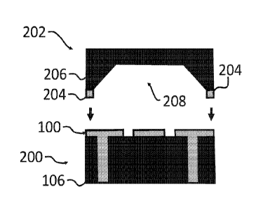
FIGS. 2A-2B are schematics that illustrate an example of establishing a local
vacuum environment for quantum circuit elements. As depicted in those figures
a chip
200 containing a superconducting quantum circuit element, such as the circuit
element
7
CA 03036945 2019-03-14
WO 2018/052414
PCMJS2016/051703
100 described with respect to FIG 1, is bonded, under vacuum, to a cap layer
202 to
form a sealed cavity 250 between the cap layer 202 and the chip 200. Though
FIGS.
2A-2B only show cross-sections, the cap layer 202 and chip 200 may be
understood to
bond to one another at regions along the y-axis (e.g., at regions that are in
and out of
the page) as well to provide a hermetic seal. The vacuum may be maintained
within
cavity 250 even though the bonded chip-cap layer structure is moved to a
higher
pressure environment, such as atmospheric pressure. Because the cap layer 202
is
bonded to the chip 200 under vacuum, adsorbates that normally would be present
under
atmospheric pressure are unavailable to weakly bind to the exposed surfaces of
the
quantum circuit element 100. Furthermore, by hermetically bonding the cap
layer 202
to chip 200, the cavity 250 is sealed so that adsorbates cannot enter.
The cap layer 202 includes a substrate 206 and a bonding layer 204 on a
surface
of the substrate 206. The substrate 206 may include, e.g., a silicon or
sapphire wafer or
portion of a wafer. The bonding layer 204 may include, for example, a
superconducting
material such as aluminum or niobium that bonds to a corresponding positioned
material on the chip 200. Other materials, such as indium or tin, also may be
used. For
improved bonding, the material of the bonding layer 204 should be the same as
the
material to which it will bond in the chip 200. For example, both materials
may include
the same superconductor. The material on chip 200 to which layer 204 bonds may
include a portion of the circuit element 100. For example, layer 204 may bond
to a
ground plane. Alternatively, the material on chip 200 to which layer 204 bonds
may be
separate from (e.g., physically and electrically separate from) the circuit
element 100.
For instance, the material on chip 200 to which layer 204 bonds can be a
separate
bonding layer.
As shown in FIGS. 2A-2B, the sealed cavity 250 may be defined by/delineated
by a concave region 208 and portions of the exposed surfaces of the
superconducting
quantum circuit element 100 and substrate 106 from chip 200. The concave
region 208
may be formed within cap layer 202 by a combination of photolithography and
etching.
For example, photolithography may be used to define a region of the substrate
206 for
etching. The defined region of the substrate 206 then may be partially etched
using
either a dry (e.g., reactive ion etching) or wet etching (e.g., KOH)
technique. The etch
time may be adjusted to vary the height of the concave region, and thus also
define the
8
CA 03036945 2019-03-14
WO 2018/052414
PCMJS2016/051703
height d of the cavity 250. The distance between a surface of the chip layer
that faces
the quantum circuit element may be, e.g., at least 1 micron, at least 5
microns, at least
microns, at least 20 microns, at least 50 microns, at least 100 microns, at
least 250
microns, at least 500 microns. Other distances are possible as well.
5 Alternatively or in addition, in some implementations, the quantum
circuit
elements may be formed in a concave region of the chip. For instance, FIG 3 is
a
schematic that illustrates an example of establishing a local vacuum cavity
for a chip
300 containing a quantum circuit element, such as circuit element 100 shown in
FIG. 1,
in which the quantum circuit element 100 may be formed within a concave region
308
10 of the chip 300. The concave region 308 may be fabricated in a similar
manner to
region 208, as described above. Though not shown in FIG 3, the cap layer 302
may
also include a concave region that aligns over and with the concave region 308
of the
chip 300 upon bonding. Bonding layers 304 may be provided on each of the cap
layer
302 and the chip 300. Bonding layers 304 may include, e.g., a material that
exhibits
superconducting properties when cooled to below a corresponding critical
temperature,
such as aluminum, niobium or titanium nitride. When joining the cap layer 302
to chip
300, the layers 304 bond to one another and form a hermetic seal of the
cavity.
Alternatively, in some implementations, the region forming the sealed cavity
may be defined without having to etch a concave region in either the chip or
the cap
layer. For example, one or more layers of material may be added to the cap
layer and/or
to the chip to form the walls of the cavity region. An example cross-section
of such a
structure is shown in FIG 4, which is a schematic that illustrates an example
of
establishing a local vacuum cavity for a chip 400 containing a quantum circuit
element,
such as the circuit 100 shown in FIG 1. As shown in FIG 4, a thickness of the
bonding
layer 404 may be increased to create a space/cavity region between the
structure 100
and a surface of the substrate 406 facing chip 400. For example, the bonding
laver 404
may have a thickness of about several microns to several tens of microns.
Instead of
increasing the thickness of the bonding layer 404 to create the cavity region,
an
alternative approach includes adding one or more layers of material to the
surface of
substrate 406 and/or to the chip 400 (e.g., through deposition or bonding),
patterning
those added layers to form the cavity walls and cavity region, and then
forming the
bonding layer on the walls.
9
CA 03036945 2019-03-14
WO 2018/052414
PCMJS2016/051703
Referring to FIGS. 2A-2B, the process of bonding the cap layer 202 to the chip
200 containing the quantum circuit element 100 will now be described. After
forming
the quantum circuit element 100 and the bonding layer 204, the exposed
surfaces of the
cap layer 202 (e.g., the bonding layer 204) and of the chip 200 (e.g., the
ground lines
associated of the quantum circuit element 100) are prepared for joining. In
some
implementations, preparation of the exposed surfaces includes performing ion
milling
of the bonding layer 204 and the corresponding material on chip 200 to which
the
bonding layer 204 adheres. Ion milling includes directing ions (e.g., argon
ions) at the
surface of the exposed layer at an acute or obtuse angle and sputtering
material from
the surface. For example, in some implementations, ion milling can be
performed in an
ion milling machine by flowing Ar gas at about 3.6 sccm at a pressure of
3.7*10'
mBar, without heat being added (e.g., under an ambient temperature of a
manufacturing
facility in which the device is being fabricated). When ion milling is applied
to a
superconductor, it is believed that the ion milling activates the surface
structure of the
superconductor to provide improved bonding properties. That is, ion milling
removes
the native oxides and/or contaminants (e.g., photoresist residues) from the
surface of
the superconductor material such that a room temperature or near room
temperature
wafer bonding can be achieved (e.g., at about an ambient temperature of the
manufacturing facility in which the device is fabricated). Removal of the
native oxide
and/or contaminants also may provide, in some implementations, the additional
advantage of reducing the presence of lossy dielectrics that lead to
dissipation/energy
loss in the system, resulting in an improvement in quality factor for the
circuit
elements.
Following the ion mill activation of the surfaces of the chip 200 and the cap
layer 202, the chip 200 and cap layer 202 are joined together. Joining the
chip 200 to
the cap layer 202 may include, for example, bonding the chip 200 to the cap
layer 202.
Bonding may include a direct bond of the bonding layer 204 on the cap layer
202 to a
corresponding bonding material on the chip 200. The bonding process may be a
direct
bonding process, in which there is no intervening layer between the bonding
layer 204
and the corresponding bonding material on the chip 200. The bonding process
may be a
cold welding process in which the bonding layer 204 is joined with the
corresponding
bonding material on the chip 200 without the use of heat, by forcing the two
CA 03036945 2019-03-14
WO 2018/052414
PCMJS2016/051703
components together with applied pressure. The bonding process may be an
indirect
bonding process, in which an adhesive is applied to the bonding layer 204
and/or to the
corresponding bonding material on the chip 200. The adhesive may include,
e.g., a
polymer that is cured after contacting the chip 200 to the cap layer 204.
In the example of FIGS. 2A-2B, the cap layer 202 is joined to the chip 200 by
bringing the bonding layer 204, which may be a superconductor material, into
direct
contact with the ground planes of the quantum circuit element 100, which may
also
include the same or different superconductor material. Preferably, both the
cap layer
202 and chip 200 are maintained under vacuum following the ion milling through
the
bonding step. The range of pressure for the vacuum can be between
approximately 10-7
Ton to approximately 10-9 Ton. After bonding, the pressure within the sealed
cavity
will be substantially the same as the pressure of the vacuum environment
during
bonding.
Joining the chip 200 to the cap layer 202 may require relatively little
pressure.
For instance, a few pounds of pressure (for a wafer of approximately 3 inch
diameter,
e.g., about a few kPa) may be sufficient to obtain an adequate bond between
the chip
200 and the cap layer 202 as in a cold-welding process. For example, to
achieve
adequate bonding, the applied pressure (applied, e.g., in a direction
orthogonal to the
surfaces being bonded) can be a non-zero pressure that is less than or equal
to 1 kPa,
less than or equal to 2 kPa, less than or equal to 3 kPa, less than or equal
to 4 kPa, less
than or equal to 5 kPa, less than or equal to 6 kPa, less than or equal to 7
kPa, less than
or equal to 8 kPa, or less than or equal to 9 kPa, among other pressures. In
some
implementations, however, greater pressure may be applied.
The joining of chip 200 and cap layer 204 also may be performed at an ambient
temperature of the manufacturing facility in which the device is constructed
(e.g., in the
range of approximately 18 C and approximately 30 C). An advantage of j
oining (e.g.,
bonding) the cap layer 202 and chip 200 without adding heat, may be that the
formation
of hillocks and voids, and the diffusion that might otherwise occur, are
absent within
the device materials, so that the circuit components can maintain low loss. In
addition,
the absence of heat being applied during the bonding process also may, in some
implementations, prevent an increase in loss that would occur at the bonding
interface
between the cap layer 202 and the chip 200. In some implementations,
additional heat
11
CA 03036945 2019-03-14
WO 2018/052414
PCMJS2016/051703
can be applied during the bonding process if desired. However, the temperature
should
preferably be kept below approximately 150 C, which is the typical
temperature at
which the hillocks and/or voids begin to form and diffusion across interfaces
increases
sufficiently enough to generate noticeable losses at the interfaces between
dielectrics
and superconductors and between superconductors. For example, the bonding
process
can be performed between approximately 18 C and approximately 150 C, such as
between approximately 100 C and approximately 150 C, between approximately
18
C and approximately 100 C, or between approximately 18 C and approximately
30
C. An approximate temperature value can have a measurement uncertainty within
plus
or minus 1 degree of the stated temperature. The relatively low temperature
bonding
can be performed using, e.g., the Bond Meister available from Mitsubishi Heavy
Industries, Ltd.
The ion milling process that is used to enhance bonding and remove native
oxides may, in certain instances, actually damage the surface of materials
that, unlike
the native oxides, are intended to form a part of quantum circuit elements or
other
components in the chip 200. These materials may include, e.g., the substrate
106 (e.g.,
Si or sapphire substrate). To moderate or removed the damaged dielectric
portions, an
additional XeF2 etch may be introduced subsequent to the ion milling and prior
to
bonding. For instance, in some implementations, the chip 200 and/or cap layer
202 may
be transferred to a XeF2 etch system after performing the ion milling. In the
XeF2 etch
system, the devices are exposed to XeF2 gas, which adsorbs to the dielectric
surface. In
the case of Si as the dielectric, the XeF2 then dissociates to Xe and F, which
in turn
forms highly volatile SiF4 that can be removed under low pressure, and thus
removes
the damaged silicon. In some implementations, the XeF2 may even improve the
reactivity of the superconductor surfaces, leading to stronger bonding. The
XeF2 etch
may be conducted under vacuum pressures in the, e.g., mTorr -Torr regime. The
etch
may also be conducted between about room temperature (e.g., about 25 C) to
about
100 C.
Another advantage of removing native oxides from the superconductor and/or
metal layers of the chip 200 and/or cap layer 202 may be that, in some
implementations, adsorbates tend to strongly bond to the surfaces from which
the
native oxides have been removed. Thus, adsorbates within the sealed cavity
that have
12
CA 03036945 2019-03-14
WO 2018/052414
PCMJS2016/051703
not been removed by the vacuum environment prior to bonding are more likely to
strongly bond to the surfaces of the superconductor and/or metal materials
than to
weakly bond to a dielectric, further reducing frequency noise. That is to say,
the
surfaces of the superconductors and/or metals from which a native oxide has
been
removed serve as getters for the adsorbates.
The use of superconductor and/or metal surfaces, from which a native oxide has
been removed, as a getter may be leveraged by increasing the surface area of
such
material within the sealed cavity. That is, additional layers of
superconductor and/or
metal layers may be formed on unused regions of the cap layer 202 and/or chip
200 that
face the cavity. By increasing the surface area of superconductor and/or metal
material
that acts as a getter, more adsorbates may be removed from the cavity (e.g.,
by strongly
binding to the additional getter material), further reducing frequency noise.
For example, the bonding layer on the cap layer surface may be extended to
increase the surface area useable as a getter, as shown in FIG. 5A. FIG. 5A is
a
schematic that illustrates an example of establishing a local vacuum cavity
for a chip
500 containing a quantum circuit element, such as circuit element 100 shown in
FIG. 1,
in which the circuit element 100 is formed on substrate 206 of chip 500. The
chip 500
may be bonded to a cap layer 502 that includes a corresponding substrate 506
and
bonding layer 504. In contrast to the bonding layer 204 of FIG. 2A, the
surface
coverage of the bonding layer 504 may be increased to provide an additional
area 510
that extends over the entire surface of the substrate 506 that faces the chip
500, rather
than being limited to just the regions that are intended to join with the chip
500 In
some implementations, adsorbates remaining in the sealed cavity preferentially
bind to
the increased surface area 510 of the bonding layer 504, leading to an
improvement in
quality factor of circuit elements formed on the chip 500.
It is not necessary for the additional getter material to be integrally
connected to
the bonding layer as shown in FIG. 5A. For example, in some implementations,
the
additional material to be used as a getter layer may be formed separately from
the
bonding layer 504. FIG. 5B is a schematic that illustrates an example of
establishing a
local vacuum cavity for a chip 500 containing a quantum circuit element, such
as
circuit element 100 shown in FIG. 1, in which an additional getter layer 512
is formed
on a surface of cap layer 502. The additional getter layer 512 again performs
the
13
CA 03036945 2019-03-14
WO 2018/052414
PCMJS2016/051703
function of providing a surface to which adsorbates will preferentially bind.
The getter
layer 512 may be formed from the same material as the bonding layer 504 or may
be
formed from a different material, such as a material that more strongly binds
to
adsorbates than the material that forms the bonding layer 504. For example,
the getter
layer 512 may be formed from titanium or a zirconium vanadium titanium alloy.
Other
materials may be used as well, such as aluminum, titanium, niobium, or
silicon. The
getter layer 512 may be formed on the cap layer 502 as shown in FIG. 5B and/or
the
getter layer 512 may be formed on regions of the chip 500 surface that face
the sealed
cavity and that are not being utilized by circuit elements.
In some implementations, the ability of the getter layer 512 (or the bonding
layer 504 as shown in FIG. 5A) to bind to adsorbates that are within the
sealed cavity
may be improved by roughening the surface of the getter layer 512. By
roughening the
surface of the getter layer 512, the surface area to which the adsorbates may
bind
increases, resulting in a greater concentration of adsorbates binding to the
getter layer
512. Various different techniques are available to roughen the surface of the
getter layer
512. For example, in some implementations, the surface of the getter layer 512
may be
roughened using etching processes, such as ion milling or the XeF2 etch. For
example,
XeF2 etching of silicon can leave a very rough surface upon which the getter
can be
deposited. The roughness is caused by the etching occurring at the molecular
level
providing a roughness at various different length scales and therefore much
more
surface area then an atomically smooth Si surface on a Si wafer that may
otherwise be
obtained directly from a manufacturer.
In the implementations disclosed herein, deposition of dielectrics,
superconductors, and/or metals can be performed using, e.g., a physical vapor
.. deposition process such as sputtering, thermal evaporation, or e-beam
deposition. Other
deposition processes may be used instead. The thickness of the deposited
superconductor layers can be selected based on the desired end use for the
superconductor (e.g., whether the layer will be part of a ground plane, a
plate of a
capacitor, a routing wire, a microstrip, a resonator, or other component). As
an
.. example the thickness of the superconductor layer can range between about 1
nm to
about 1 micron, though other thicknesses are also possible.
14
CA 03036945 2019-03-14
WO 2018/052414
PCMJS2016/051703
Processes described herein may entail the deposition of one or more materials,
such as superconductors, dielectrics and/or metals. Depending on the selected
material,
these materials may be deposited using deposition processes such as chemical
vapor
deposition, physical vapor deposition (e.g., evaporation or sputtering), or
epitaxial
.. techniques, among other deposition processes. Processes described herein
may also
entail the removal of one or more materials from a device during fabrication.
Depending on the material to be removed, the removal process may include,
e.g., wet
etching techniques, dry etching techniques, or lift-off processes.
Implementations of the quantum subject matter and quantum operations
described in this specification may be implemented in suitable quantum
circuitry or,
more generally, quantum computational systems, including the structures
disclosed in
this specification and their structural equivalents, or in combinations of one
or more of
them. The term -quantum computational systems" may include, but is not limited
to,
quantum computers, quantum information processing systems, quantum
cryptography
systems, or quantum simulators.
The terms quantum information and quantum data refer to information or data
that is carried by, held or stored in quantum systems, where the smallest non-
trivial
system is a qubit, e.g., a system that defines the unit of quantum
information. It is
understood that the term `-qubit" encompasses all quantum systems that may be
suitably
approximated as a two-level system in the corresponding context. Such quantum
systems may include multi-level systems, e.g., with two or more levels. By way
of
example, such systems can include atoms, electrons, photons, ions or
superconducting
qubits. In many implementations the computational basis states are identified
with the
ground and first excited states, however it is understood that other setups
where the
computational states are identified with higher level excited states are
possible. It is
understood that quantum memories are devices that can store quantum data for a
long
time with high fidelity and efficiency, e.g., light-matter interfaces where
light is used
for transmission and matter for storing and preserving the quantum features of
quantum
data such as superposition or quantum coherence.
Quantum circuit elements may be used to perform quantum processing
operations. That is, the quantum circuit elements may be configured to make
use of
quantum-mechanical phenomena, such as superposition and entanglement, to
perform
CA 03036945 2019-03-14
WO 2018/052414
PCT/1JS2016/051703
operations on data in a non-deterministic manner. Certain quantum circuit
elements,
such as qubits, may be configured to represent and operate on information in
more than
one state simultaneously. Examples of superconducting quantum circuit elements
that
may be formed with the processes disclosed herein include circuit elements
such as co-
planar waveguides, quantum LC oscillators, qubits (e.g., flux qubits or charge
qubits),
superconducting quantum interference devices (SQUIDs) (e.g., RF-S QUID or DC-
SQUID), inductors, capacitors, transmission lines, ground planes, among
others.
In contrast, classical circuit elements generally process data in a
deterministic
manner. Classical circuit elements may be configured to collectively carry out
instructions of a computer program by performing basic arithmetical, logical,
and/or
input/output operations on data, in which the data is represented in analog or
digital
form. In some implementations, classical circuit elements may be used to
transmit data
to andior receive data from the quantum circuit elements through electrical or
electromagnetic connections. Examples of classical circuit elements that may
be
formed with the processes disclosed herein include rapid single flux quantum
(RSFQ)
devices, reciprocal quantum logic (RQL) devices and ERSFQ devices, which are
an
energy-efficient version of RSFQ that does not use bias resistors. Other
classical circuit
elements may be formed with the processes disclosed herein as well.
During operation of a quantum computational system that uses superconducting
quantum circuit elements and/or superconducting classical circuit elements,
such as the
circuit elements described herein, the superconducting circuit elements are
cooled
down within a cryostat to temperatures that allow a superconductor material to
exhibit
superconducting properties.
While this specification contains many specific implementation details, these
should not be construed as limitations on the scope of what may be claimed,
but rather
as descriptions of features that may be specific to particular
implementations. Certain
features that are described in this specification in the context of separate
implementations can also be implemented in combination in a single
implementation.
Conversely, various features that are described in the context of a single
implementation can also be implemented in multiple implementations separately
or in
any suitable sub-combination. Moreover, although features may be described
above as
acting in certain combinations and even initially claimed as such, one or more
features
16
CA 03036945 2019-03-14
WO 2018/052414
PCT/1JS2016/051703
from a claimed combination can in some cases be excised from the combination,
and
the claimed combination may be directed to a sub-combination or variation of a
sub-
combination.
Similarly, while operations are depicted in the drawings in a particular
order,
this should not be understood as requiring that such operations be performed
in the
particular order shown or in sequential order, or that all illustrated
operations be
performed, to achieve desirable results. For example, the actions recited in
the claims
can be performed in a different order and still achieve desirable results. In
certain
circumstances, multitasking and parallel processing may be advantageous.
Moreover,
the separation of various components in the implementations described above
should
not be understood as requiring such separation in all implementations.
A number of implementations have been described. Nevertheless, it will be
understood that various modifications may be made without departing from the
spirit
and scope of the invention. Accordingly, other implementations are within the
scope of
the following claims.
17