Note: Descriptions are shown in the official language in which they were submitted.
HYBRID RECTIFIER
[1]
Field
[2] The described embodiments relate to the power electronics.
Background
[3] A rectifier is a device used to convert the electrical supply provided
by a utility
company in alternating current form (AC) into the direct current form (DC)
that is needed
by some applications. Electronic rectifiers are used in most AC/DC power
supplies,
motor drives (variable frequency or servo), battery chargers, etc. Almost all
electronic
devices powered by an electrical distribution network use a rectifier. There
are many
types of rectifiers from simple to complex ones, each offering difference
levels of
performance.
[4] Typically, the simplest rectifiers use a number of diodes. These diode
rectifiers
have the characteristic of producing a significant level of current
distortion, which is
unacceptable for some applications, such as those that are subject to
regulations or
standards such as IEEE 519.
[5] Active rectifiers have been developed in order to achieve better levels
of current
distortion than diode rectifiers. Traditionally, the goal has been to
significantly reduce
distortion beyond the limits set out by regulations and standards. Active
rectifiers are
more complex than diode rectifiers, and use active switches (typically
transistors) to
control the flow of current. However, active rectifiers have an associated
cost that is
higher than a diode rectifier, since the transistors used must be capable of
conducting
relatively high current, which makes them expensive.
[6] Furthermore, active rectifiers typically have low efficiency at partial
loads, due to
the continual switching of the transistors, which produces losses even when
the load
goes to zero. For some applications and industries, the efficiency of known
active
rectifiers is unacceptably low, or, at the very least, represents a
substantial problem.
¨1-
3543472
CA 3039076 2019-11-21
CA 03039076 2019-04-02
WO 2018/072016 PCT/CA2017/051232
Summary
[7] In a first aspect, some embodiments of the invention provide a hybrid
rectifier
circuit for rectifying an alternating current. For each AC phase, the hybrid
rectifier circuit
comprises a top diode for conducting current during a positive current portion
of the
alternating current and a top transistor connected in parallel to the top
diode. The hybrid
rectifier further comprises a bottom diode for conducting current during a
negative
current portion of the alternating current and a bottom transistor connected
in parallel to
the bottom diode. A hybrid rectifier controller is connected to the top
transistor and the
bottom transistor for switching the top transistor and the bottom transistor.
According to
some embodiments, the control can be designed in order to keep the transistor
switching to a minimum. During the positive current portion of the alternating
current,
the bottom transistor is switched so that the bottom transistor conducts
current when the
current through the top diode is below a sinusoidal reference current, the
bottom
transistor is switched so that the bottom transistor does not conduct current
when the
current through the top diode is above the sinusoidal reference current.
Similarly, during
the negative current portion of the alternating current, the top transistor is
switched so
that the top transistor conducts current when the current through the bottom
diode is
above the sinusoidal reference current, and the top transistor is switched so
that the top
transistor does not conduct current when the current through the bottom diode
is below
the sinusoidal reference current.
[8] According to some embodiments, the hybrid rectifier can be implemented
as a
three-phase hybrid rectifier, with a top transistor, top diode, bottom
transistor, bottom
diode, and hybrid-rectifier controller for each phase.
[9] In a second aspect, some embodiments of the invention provide a hybrid
rectifier
circuit for rectifying an alternating current. The hybrid rectifier circuit
comprises a top
transistor for conducting current during a positive current portion of the
alternating
current and switching during negative current portion of the alternating
current. The
hybrid rectifier circuit further comprises a bottom transistor for conducting
current during
the negative current portion of the alternating current and switching during
the positive
current portion of the alternating current. A hybrid-rectifier controller is
connected to
each of the top and bottom transistor for switching the bottom transistor
during the
¨2¨
CA 03039076 2019-04-02
WO 2018/072016 PCT/CA2017/051232
positive portion of the alternating current when the current through the top
transistor is
below a sinusoidal reference current, and switching the top transistor during
the
negative portion of the alternating current when the current through the
bottom
transistor is above the sinusoidal reference current.
[10] According to some embodiments, the transistors in the hybrid rectifier
may be
field-effect transistors (FETs).
[11] In a third aspect, some embodiments of the invention provide a hybrid
rectifier
circuit for power regeneration. The hybrid rectifier circuit comprises a top
diode for
conducting freewheeling current during a positive current portion of the
alternating
current and a top transistor connected in parallel to the top diode. The
hybrid rectifier
circuit further comprises a bottom diode for conducting freewheeling current
during a
negative current portion of the alternating current and a bottom transistor
connected in
parallel to the bottom diode. A hybrid-rectifier controller is connected to
the top
transistor and the bottom transistor such that, during the positive current
portion of the
alternating current, the bottom transistor is switched so that the bottom
transistor
conducts current when the current through the bottom transistor is below a
sinusoidal
reference current, and the bottom transistor is switched so that the bottom
transistor
does not conduct current when the current through the bottom transistor is
above the
sinusoidal reference current. During the negative current portion of the
alternating
current, the bottom transistor is switched so that the top transistor conducts
current
when the current through the top transistor is above the sinusoidal reference
current,
and the top transistor is switched so that the top transistor does not conduct
current
when the current through the top transistor is below the sinusoidal reference
current.
[12] In a fourth aspect, some embodiment of the invention provide a hybrid
rectifier for
filtering harmonics of a parallel high-power rectifier, comprising a hybrid
rectifier
connected in parallel to the high-power rectifier.
Brief Description of the Drawings
[13] A preferred embodiment of the present invention will now be described in
detail
with reference to the drawings, in which:
FIG. 1 is a circuit diagram of a hybrid rectifier according to some
embodiments;
¨3¨
CA 03039076 2019-04-02
WO 2018/072016 PCT/CA2017/051232
FIG. 2 depicts curves of current conduction of a 3-phase hybrid rectifier
according to some embodiments;
FIG. 3, is a schematic of a hybrid-rectifier controller according to some
embodiments;
FIG. 4 depicts a DC bus voltage ripple, as may be used by a hybrid-rectifier
controller according to some embodiments;
FIG. 5 depicts voltage and current curves during a load-dump protection,
according to some embodiments;
FIG. 6 depicts voltage and current curves showing the current through the
diodes
.. and transistors of a hybrid rectifier according to some embodiments;
FIG. 7 is a circuit diagram of a hybrid rectifier using FETs according to some
embodiments;
FIG. 8 is a circuit diagram depicting current flow during the operation of a
hybrid
rectifier using FETs in parallel with diodes, according to some embodiments;
FIG. 9 is a circuit diagram depicting current flow during the operation of a
hybrid
rectifier using only FETs (and no diodes in parallel), according to some
embodiments;
FIG. 10 depicts curves of current conduction of a 3-phase hybrid rectifier
using
FETs according to some embodiments;
FIG. 11 is a circuit diagram of a hybrid rectifier used as a harmonic filter
for a
large rectifier according to some embodiments; and
FIG. 12 depicts curves showing average diode forward voltage drop for a
typical
300A rectifier.
Description of Exemplary Embodiments
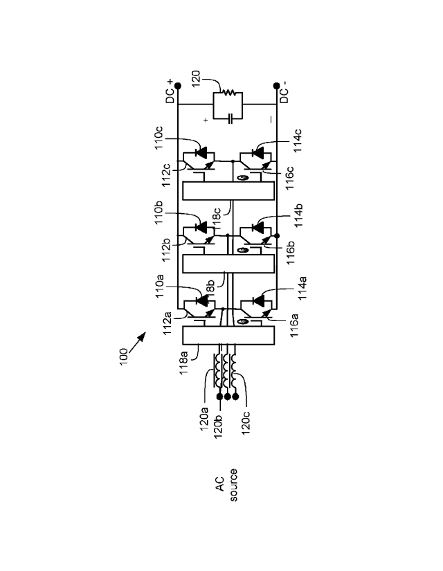
[14] Referring to FIG. 1, there is shown a circuit diagram of a hybrid
rectifier 100.
Generally, the hybrid rectifier 100 mitigates the problems presented by known
active
rectifiers and diode rectifiers by combining the strengths of a diode
rectifier and the
strengths of an active rectifier. While the schematic diagram of the hybrid
rectifier 100
bears some similarity to a known active rectifier, it is important to
understand that the
component sizing for the hybrid rectifier is different than for an active
rectifier. As such,
¨4¨
CA 03039076 2019-04-02
WO 2018/072016 PCT/CA2017/051232
the hybrid rectifier produces fewer losses as compared to an active rectifier,
while, at
the same time, providing improved efficiency.
[15] In particular, a significant difference between the hybrid rectifier 100
and a known
active rectifier is the control technique. Contrary to the active rectifier,
the simpler phase
by phase control circuit of the hybrid rectifier can be embedded for each
phase leg of a
multi-phase rectifier, thereby eliminating the isolated signal usually needed
for an active
rectifier. Any known phase current and DC bus voltage sensor can be used as
the
implementation is not critical to the operation.
[16] The hybrid rectifier 100 is shown as a three-phase hybrid rectifier, and
the
nomenclature "a", "b", and "c" is used to denote each of the three phases.
According to
some embodiments, a single-phase hybrid rectifier may be used, for example,
comprising one (or two) of the component sets "a", "b", or "c" corresponding
to a single
phase in the hybrid rectifier 100.
[17] The hybrid rectifier 100 comprises atop diode 110a in parallel with atop
transistor 112a, which together form a top switch. The bottom switch comprises
a
bottom diode 114a in parallel with a bottom transistor 116a as shown. The
diodes 110a
and 114a with the transistors 112a and 116a correspond to one phase of the
three-
phase hybrid rectifier 100. Similarly, the hybrid rectifier 100 comprises
diodes
110b,110c, 114b, 114c and transistors 112b,112c, 116b, 116c, corresponding to
the
.. other two phases..
[18] As used herein, the term "transistor" is used to represent a fast
semiconductor
switch capable of being commutated on and off at will, for example, but not
limited to a
bipolar junction transistor (BJT), an insulated-gate bipolar transistor
(IGBT), any type of
field effect transistor (FET) such as; metal-oxide-semiconductor field-effect-
transistor
(MOSFET), or junction gate field effect transistor (JFET), a gate turn-off
thyristor (GTO),
and a forced-commutated thyristor. A person skilled in the art will appreciate
that other
devices may be used as well.
[19] As used herein, the terms "top" and "bottom" are used in respect of the
components on a rectifier schematic (e.g. top rectifier switch, top diode, top
transistor,
bottom rectifier switch, bottom diode, bottom transistor). As will be
appreciated by a
person skilled in the art, the terms "top" and "bottom" generally refer to the
role of a
¨5¨
CA 03039076 2019-04-02
WO 2018/072016 PCT/CA2017/051232
component as a rectifier, and not to a specific circuit layout or topology.
For example, a
"top diode" is used to rectify the positive current portion (i.e. half cycle)
of an alternating
current, regardless of any particular physical layout of the components.
[20] A hybrid-rectifier controller 118a is connected to both the top
transistor 112a and
the bottom transistor 116a in order to control the state of the transistors.
As shown in
FIG. 1 (an IGBT transistor is shown by way of example), the hybrid-rectifier
controller
118a is connected to the gate of the top transistor 112a and the gate of the
bottom
transistor 116a. It will be appreciate that, for other types of transistors,
the hybrid-
rectifier controller 118a may be connected accordingly, such as to the base of
a
transistor instead of the gate. As described herein, with this circuit
topology, the hybrid-
rectifier controller 118a can be used to operate the hybrid rectifier 100
between a simple
diode-rectifier mode and a more complex active-rectifier mode. According to
some
embodiments, the hybrid rectifier 100 can be used by switching between these
modes,
thereby improving the harmonic-distortion issues of simple diode rectifiers
while being
simpler to implement and/or less expensive than an active rectifier
[21] As previously described the hybrid rectifier can be implemented as a
three-phase
hybrid rectifier, such as the hybrid rectifier 110 shown in FIG. 1. In the
three-phase
case, separate hybrid-rectifier controllers (e.g. hybrid-rectifier controllers
118a, 118b,
and 118c) are used for each phase. In this case, multiple controllers may be
mounted
on a single circuit board if desired. Furthermore, the hybrid rectifier can be
used for
multi-level rectifiers as well. Alternatively, according to some embodiments,
a single
hybrid-rectifier controller may be used to control more than one phase.
[22] The hybrid-rectifier controller 118a can be used to implement a switching
strategy for the transistors that keeps the diodes as the main rectification
elements. In
this case, both the top rectifier switch and the bottom rectifier switch are
made by
combining diodes with transistor, and using the diodes as the main
rectification element.
This is in contrast to known active rectifiers, in which transistors are the
main
rectification element.
[23] In other words, the control strategy disclosed herein relies on a
different
operation of the components as compared to known active rectifiers. According
to the
control strategy used for the hybrid rectifier, the transistors are only used
to direct the
¨6¨
CA 03039076 2019-04-02
WO 2018/072016 PCT/CA2017/051232
current in the diodes when the phase current would normally be lower than
desired (e.g.
as compared to a desired reference current). In the case of known active
rectifiers, the
DC bus voltage needs to be boosted by at least 10% to 30% above the diode
rectifier's
level to operate, whereas with the hybrid rectifier, the transistors switch
intermittently
and the DC bus voltage is kept at a lower average value very close to the
diode
rectifier's level.
[24] In some embodiments, the hybrid rectifier can retain many of the
characteristics
of the active rectifier, but with lower losses and/or a lower cost similar to
the diode
rectifier. For example, the hybrid rectifier can have lower switching and
conduction
losses than the active "boost" rectifier, and can be more efficient,
especially at lower
power, where the efficiency of active rectifiers is dramatically reduced.
[25] Furthermore, the transistors in the hybrid rectifier may not be affected
by dead
time or shoot through due to the single polarity modulation. Thus, slow turn-
off devices
can be used, since they usually produce lower conduction losses.
[26] Another aspect of the hybrid rectifier, in some cases, is a lower EMI and
ripple-
current emission as compared to an active rectifier, due to a reduced number
of
switching events, and/or switching events occurring at lower currents.
Furthermore, the
hybrid rectifier may have a smaller DC bus capacitance as compared to an
active
rectifier, which can be used to maintain stability or to reduce the DC voltage
ripple of the
diode rectifier.
[27] According to some embodiments, the hybrid rectifier may be built using
smaller
transistors than those necessary in an active rectifier, thus leading to cost
reduction of
the hybrid rectifier as compared to an active rectifier.
[28] While the hybrid rectifier may be implemented to have improved efficiency
over
an active rectifier, it may also be implemented to have lower current
distortion
(harmonics) than a diode rectifier. In other words, the control strategy can
be
implemented in order to limit the distortion to an acceptable level while
minimizing the
transistor conduction and switching losses.
[29] Furthermore, the hybrid rectifier can be implemented to have a smoother
DC bus
voltage than a diode rectifier. For example, a three-phase hybrid rectifier
may have
variation in the DC buss voltage in the range of 2% to 5% whereas the diode
rectifier
¨7¨
CA 03039076 2019-04-02
WO 2018/072016 PCT/CA2017/051232
may be around 14%. Nonetheless, the hybrid rectifier may operate with a
similar (i.e.
"low") DC bus voltage as compared to a diode rectifier, which can have the
effect of
reducing component stress.
[30] Referring to FIG. 2, there is shown a diagram depicting curves of a three-
phase
diode rectifier current 210, a sinusoidal reference current (e.g. "ideal")
212, and
conduction through the hybrid rectifier for a bottom transistor (commutation
mode) 214,
a top diode (continuous conduction mode) 216, a top transistor (commutation
mode)
218, and a bottom diode (continuous conduction mode) 220. A control strategy,
as may
be implemented by a hybrid-rectifier controller (e.g. hybrid-rectifier
controller 118a), can
be explained in reference to FIG. 2.
[31] As shown in FIG. 2, a control strategy can be determined such that,
during the
positive current portion of an alternating current through the diode rectifier
210, there is
conduction through the bottom transistor 214 whenever the line current is
below the
sinusoidal reference current 212. When the line current is above the
sinusoidal
reference current 212, then conduction is through the top diode 216.
[32] Similarly, for the negative current portion, there is conduction through
the top
transistor 218 whenever the line current is above the sinusoidal reference
current 212.
When the line current is below the sinusoidal reference current 212, then the
conduction
is through the bottom diode 220.
[33] The control strategy disclosed here can be used for any or all of the
following five
objects.
[34] First, transistor switching can be kept to a minimum, and mostly in the
region of
the line cycle, where low amplitude line current flows. This can be seen in
the
conduction of the bottom transistor 214 and the top transistor 218 in FIG. 2.
According
to some embodiments, this can reduce the commutation losses in the
transistors,
diodes, and line inductors.
[35] Second, in reference to the conduction of the top diode 216 and the
bottom diode
220, most of the high current conduction is done by the diodes that generally
have lower
conduction losses than the transistors.
[36] Third, packaging the circuit (e.g. including the rectifier switches and
an
associated hybrid-rectifier controller) can be facilitated since the controls
are relatively
¨8¨
CA 03039076 2019-04-02
WO 2018/072016 PCT/CA2017/051232
simple (e.g. as compared to an active rectifier), such that each pair of
transistors and
diodes (i.e. the top rectifier switch and the bottom rectifier switch for a
single phase)
operate independently.
[37] Fourth, the harmonic levels produced by the hybrid rectifier can be
managed, for
example, in regards to a particular regulation such as IEEE 519. According to
some
embodiments, achieving better harmonic levels than proscribed by a particular
regulation are not necessary.
[38] Fifth, DC bus voltage ripple can be kept in line with that of an active
rectifier,
which is significantly lower than a diode rectifier. The effect of this is a
reduction in the
current distortion through the load.
[39] According to some embodiments, the control strategy can use the line
inductors
(e.g. line inductors 120a, 120b, and 120c) and the transistor pulses to
maintain the total
current distortion demand (TDD-I) to an acceptable level.
[40] In a simplified control strategy, the hybrid-rectifier controller doesn't
need a
precise synchronization with the line, which makes it more robust as compared
to an
active rectifier. In this case, the current reference is simply extracted from
the line
voltage.
[41] In some cases, a pre-programmed control strategy can be used. This can be
accomplished with a transistor switching pattern that can be adjusted with a
simple
feedback. For example, feedback from the line current as to adapt to the
loading of the
rectifier. Alternatively, the DC voltage with respect to the line voltage can
be used to
avoid entering the boosting mode (i.e. of an active rectifier) while reducing
the DC
voltage ripple.
[42] Furthermore, a more elaborate control strategy can be used, which
generates the
transistor switching command in real time using the line voltage polarity and
compares
the line current amplitude to a reference. In this case, transistor switching
occurs when
the line current amplitude is lower than the reference. Essentially, the
transistors
maintain the current when it would be lower than the sinusoidal reference with
a diode
rectifier.
[43] According to some embodiments, the hybrid-rectifier controller can be
implemented with a PID (or similar) controller and basic logic in order to
control the
¨9¨
CA 03039076 2019-04-02
WO 2018/072016 PCT/CA2017/051232
transistor pulse widths. More complex hybrid-rectifier controllers may be
based on
vector control, dead-beat control, or other advanced methods used to optimize
the
tradeoff between switching losses and the generation of harmonics.
[44] Referring to FIG. 3, there is shown a schematic of a simple hybrid-
rectifier
controller 300, such as may be used for each phase to provide independent
control to
that phase. The controller uses a voltage comparator 310 and an inverter 312
to only
enable operation of the bottom transistors through the positive current
controller 314
during the positive half-cycle and only the top transistors through the
negative current
controller 316 during the negative half cycle.
[45] The hybrid rectifier controller 300 includes both a positive current
controller 314
and a negative current controller 316, though only the details of the positive
current
controller 314 are shown. The analogous components of the negative current
controller
316 are not shown in FIG. 3.
[46] The transistor switching (e.g. the bottom transistor switching through
the positive
current controller 314) is activated when the diode current 318 is below a
sinusoidal
reference current 320. The sinusoidal reference current 320 may be generated
to be in
phase with the line voltage, as depicted in FIG. 2. A pulse-width modulator
322 is used
to increase the pulse-width modulation (PWM) when the diode current 318 is
below the
sinusoidal reference current 320 (see also: the diode current 210 and the
sinusoidal
reference current 212 in FIG. 2) in order to sustain the current. The PWM is
reduced to
zero when diode current 318 is above the sinusoidal reference current 320 in
order to
stop the transistors.
[47] A simple PI or P ID error amplifier 324 can be used for the controller.
In some
application, a pre-programmed switching pattern that adapts to the load can be
used.
Other common error amplifier topologies can be suited for this application as
well.
[48] While the transistor switching can be accomplished using a pulse-width
modulator 322, for example, by modulating the pulse width according to the
output of
the PID 324, other transistor switching schemes can also be used. For example,
a
hysteresis controller may be used to control the transistor switching.
¨10¨
CA 03039076 2019-04-02
WO 2018/072016 PCT/CA2017/051232
[49] The amplitude of the sinusoidal reference current 320 can be adjusted to
generate the AC current needed to satisfy the load. According to some
embodiments,
this can be accomplished using any of the following techniques.
[50] First, the line or the load current can be measured to derive the
equivalent
sinusoidal line current.
[51] Second, the DC bus voltage can be used with respect to the line voltage.
In this
case, the amplitude of the sinusoidal reference current 320 is increased when
the DC
bus voltage is below the peak line-to-line voltage (-µ12 VLL) and decreased
when it is
above.
[52] Third, the DC bus voltage ripple can be used to adjust the amplitude of
the
sinusoidal reference current 320. The optimal amplitude of the sinusoidal
reference
current 320 can be obtained when the ripple becomes relatively small, as shown
in FIG.
4.
[53] Fourth, a pre-calculated switching pattern can be saved in memory and
simply
scaled with the diode current 318 or the DC bus voltage.
[54] According to some embodiments, some basic protections can be included in
the
hybrid rectifier, such as over-current and over-temperature protection for the
transistors,
and a switching disable level activated from the DC bus voltage.
[55] Over-current and overt-temperature protections for the transistors reduce
and
eventually stop the commutation mode. Since the diodes can still operate,
there can be
a resulting increase in the harmonic distortion. However, the rectifier still
operates, thus
yielding a high availability.
[56] A DC bus voltage protection level can be defined at a few percent above
the
expected DC voltage in order to stop the transistor switching until the DC bus
voltage
returns to an acceptable value. The ability to disable the DC bus can be used
in case of
a sudden removal of the load (load dump), where the transistor switching could
raise
the DC bus voltage to dangerous levels.
[57] The load dump protection produced disabling of the transistor switching
is
depicted in FIG. 5, in which 510 shows the DC bus voltage, 512 shows the AC
voltage,
514 shows the transistor current, 516 shows the diode current, 518 shows the
AC line
current, and 520 shows the load current.
¨11¨
CA 03039076 2019-04-02
WO 2018/072016 PCT/CA2017/051232
[58] The load dump protection relies on a simple voltage comparator to detect
the
high DC bus voltage and stop the transistor switching altogether, until it
returns to the
desired value, as shown in FIG. 5. The load dump protection can also be
combined with
energy return (regenerative) applications of a hybrid rectifier circuit. Both
the load dump
protection and the energy return activate when the DC bus to rise above their
set levels.
The first level causes the transistors to stop, while the second, higher level
triggers the
energy return switching pattern.
[59] Referring to FIG. 6, there is shown an example of the operation of one
leg in a
three-phase hybrid rectifier application. Other voltages or currents operate
in a similar
fashion.
[60] The trace 610 shows the DC bus voltage for a 220VLN / 380 VLL source.
FIG. 6
shows that the DC bus voltage is very close to the Vdc = -\12 VLL = 1.41 *380
VLL = 535
Vdc. The trace 612 shows the line voltage of 220VLN. The trace 614 shows the
current
through the bottom transistor, and the trace 616 shows the current through the
top
transistor. The trace 618 shows the top diode current, which is significantly
higher than
the current through the transistors shown in 614 and 616. The trace 620 shows
the AC
line current superimposed on the ideal current.
[61] Referring to FIG. 7, and according to some embodiments, a hybrid
rectifier 700
can be build using FETs as the top transistors 712a, 712b, 712c and bottom
transistors
716a, 716b, 716c, in order to achieve both a synchronous rectifier as well as
a current
steering switch. This type of transistor can conduct in reverse instead of, or
in parallel
with, a diode, and switch as a transistor.
[62] A hybrid rectifier built using FETs. FET transistors can be used as
synchronous
rectifiers, especially at low power, to conduct in reverse instead of the
diodes, or,
alternatively, along with the diodes. Thus, this can be used to reduce the
number of
components by eliminating the diodes (e.g. the diodes 712a, 712b, 712c, 714a,
714b,
714 shown in FIG. 7). Alternatively, the overall conduction losses can be
reduced when
operating the transistors in parallel with the diodes, as in the case of the
hybrid rectifier
700 shown in FIG. 7.
[63] According to some embodiments, a hybrid rectifier built using FETs
reduces the
number of semiconductors as compared with other rectifiers. Furthermore, when
used
¨ 12¨
CA 03039076 2019-04-02
WO 2018/072016 PCT/CA2017/051232
with the simpler control strategy, rectifier modules can be produces that take
advantage
of the FET's properties in order to reduce costs. In the case of the hybrid
rectifier
disclosed herein, the FET is used as both a rectifier and a switch, according
to the
control strategies described above.
[64] The case of a FET in parallel with a diode is shown in FIG. 8. In FIG. 8,
800
shows rectification of a current 802 through a diode 810 only, 830 shows
parallel
rectification from both a current 802 through the diode 810 and a current 804
through
the top transistor 812, and 860 shows that the top transistor 812 has been
switched to
maintain the flow of current 806. FIG. 8 depicts the positive current portion
of the
alternating current.
[65] The case of a FET hybrid rectifier without the use a diode is shown FIG.
9. In
FIG. 9, 900 shows rectification of a current 902 through the top transistor
912 and 950
shows that the top transistor 912 has been switched to maintain the flow of
current 906
through the bottom transistor 916. FIG. 9 depicts the positive current portion
of the
.. alternating current.
[66] Referring to FIG. 10, there is shown a diagram depicting curves of a
three-phase
rectifier current 1010, a sinusoidal reference current (e.g. "ideal") 1012,
and conduction
for a FET hybrid rectifier, through the top FET while the bottom FET is
switched
(commutation mode) 1014, through the top FET (continuous conduction mode)
1016,
.. through the bottom FET while the top FET is switched (commutation mode)
1018, and
through the bottom FET (continuous conduction mode) 1020. A control strategy,
as may
be implemented by a hybrid-rectifier controller (e.g. hybrid-rectifier
controller 118a),
based on FIG. 10, in a similar manner as was described for the control
strategy based
on FIG. 2.
[67] As shown in FIG. 10, a control strategy can be determined such that,
during the
positive current portion of an alternating current, the top FET rectifies the
current while
the bottom FET is switched whenever the line current is below the sinusoidal
reference
current 1012. When the line current is above the sinusoidal reference current
1012, then
conduction is through the top FET 1016. An analogous strategy is extended to
the
negative current portion of the alternating current accordingly.
¨13¨
CA 03039076 2019-04-02
WO 2018/072016 PCT/CA2017/051232
[68] A hybrid rectifier may be used for a range of applications, including
uninterruptible power supplies (UPS), large DC power supplies (e.g. for plasma
torches,
welders, radar transmitters, electrochemistry, etc.), HVDC power distribution
lines, and
battery chargers and traction supplies.
[69] Furthermore, the hybrid rectifier can be used with variable-speed drives
and
other AC/DC/AC converters with regenerative breaking and energy recovery. To
this
end, the hybrid rectifier may be suitable as a low, medium, and high-voltage
rectifier.
[70] According to some embodiments, a switching strategy can be used to return
energy to the line when the DC bus is charged by a regenerative load such as a
motor
braking. This returns the energy in the line instead of dissipating the energy
in a
dynamic braking resistor as is currently the practice for diode rectifier
applications. This
can be accomplished with a hybrid rectifier using a control strategy similar
to the simple
control strategy previously described. In this way, contrary to the current
practice using
diode rectifiers, regeneration is possible with an efficient regeneration. For
example, in a
motor drive, the dynamic braking resistors are not needed to dissipate the
braking
energy. In regeneration, the transistors do most of the work, as in an active
rectifier. The
transistors also operate in the reverse direction of the diodes in
rectification mode.
[71] In many applications, such as motor-variable drives, it may be necessary
to slow
down the motor by dissipating some of the motor's kinetic energy. The usual
technique
on a simple motor drive involved dissipating the kinetic energy in a bank of
resistors.
This represents a loss of energy, which is wasteful. More complex and
expensive active
rectifier drives have the ability to return this energy to the line with fewer
losses. With
the use of the hybrid rectifier (including the control strategies) described
here, during
regeneration, the DC voltage is allowed to increase by a few percent, thereby
blocking
the operation of the diodes. When this happens, the transistors are commutated
with a
complementary strategy to that of rectification. In other words, the top
transistors
conduct during the positive line voltage, or by using another appropriate
control
scheme.
[72] In essence, the regenerative mode of operating a hybrid rectifier can be
seen as
being the opposite (compliment) of the rectification strategies previously
described. The
regeneration mode can be activated when the DC bus voltage is at a
sufficiently-high
¨ 14¨
CA 03039076 2019-04-02
WO 2018/072016 PCT/CA2017/051232
level. In the regeneration mode, the bottom transistors commutate during the
positive
current portion of the alternating current, and the top transistors commutate
during the
negative current portion of the alternating current.
[73] Different modulation techniques may be used during the regeneration mode.
For
some applications, a pre-programmed pulse sequencing technique is sufficient.
Typically, regeneration current is relatively low and occurs for a relatively
short time,
such that harmonic distortion does not become a significant problem. This
makes a
simple control strategy acceptable. Generally, the regenerative current should
be
limited to the capacity of the transistors selected for the circuit. In cases
when full
regeneration is required or preferred, fully-rated transistors can be used in
the rectifier.
[74] According to some embodiments, the hybrid rectifier circuit can be used
as a
hybrid filter, for example, as an alternative to a parallel harmonic filter.
[75] Active harmonic filters are often produced using complete active
rectifier circuits
that include line inductors and a DC capacitor bank, in parallel with a
harmonic-
generating load. Current sensors are added to the circuit to the harmonic-
generating
load in order to measure the harmonic content so that an inverted harmonic
current can
be injected to cancel the harmonic content from the harmonic-generating load.
Various
versions of this scheme are well known, and all require a boosted independent
DC bus
voltage and a control strategy that is more complex than that of this hybrid
rectifier.
[76] Referring to FIG. 11, there is shown a hybrid rectifier circuit 1110. The
hybrid
rectifier circuit 1110 can be used as a hybrid filter in order to separate the
low
frequency, high-power rectifier components of the larger rectifier 1112 from
the hybrid
rectifier 1110 . In some cases, the control strategies previously described
for the hybrid
rectifier may be capable of providing the required filtering. Contrary to an
active
harmonic filter, the hybrid rectifier 1110 can add a regeneration capability
to the diode
rectifier. Such a configuration may be suitable for retrofitting to an
existing rectifier, or
when the high-power rectifier components are too slow to handle the high-
frequency
current pulses from the transistors.
[77] As shown in FIG. 11, the hybrid rectifier 1110 can be used as a parallel
harmonic
filter using the DC bus of the main rectifier 1112. In this case, the hybrid
rectifier 1110
and its line inductors can be connected in parallel with an existing high-
power rectifier
¨15¨
CA 03039076 2019-04-02
WO 2018/072016 PCT/CA2017/051232
1112 to minimize the harmonics through the use of the simple control strategy
of the
hybrid rectifier 1110.
[78] Furthermore, some of the simple control strategies, as previously
described,
don't require supplementary current sensors to measure the harmonics generated
by
the high-power rectifier 1112
[79] As previously provided, a hybrid rectifier may be used in order to
achieve lower
costs than an analogous active rectifier. This can be seen, for example, in
cases when
the current capacity of the transistors is much lower than that of less-
expensive diodes.
In this case, the control strategies described above are advantageous, since
they direct
most of the current conduction to the diodes for rectification, and keep the
switching
losses relatively low. In such a case, the total rectifier costs can be
reduced to between
that of an active rectifier and a diode rectifier. According to some
embodiments, each
phase of the rectifier circuit can be assembled out of discrete components on
a printed
circuit board ("PCB"), or assembled in an intelligent power module, or
produced as an
integrated circuit. Medium and high-voltage rectifiers may also benefit from
this feature,
since the transistors are very expensive at this power level.
[80] Generally speaking, for any particular hybrid rectifier, component
selection (e.g.
transistors and/or diodes) can be optimized with respect to cost and
efficiency. The
main gain in efficiency comes from a reduction in the conduction loses through
the
transistors, since most of the current conduction is transferred through the
diodes.
Another gain in efficiency may be seen based on a reduction in the transistor
switching
losses, since the transistors are switching mostly at lower current and
operating at lower
DC bus voltages. The switching losses are related to the square of the DC bus
voltage.
Thus, reducing the DC bus voltage by 15% to 20% can result in a savings of 30%
of the
switching losses.
[81] Conduction losses can also be related to the size of the components
selected.
For example, using a hybrid rectifier in a particular application rather than
an active
rectifier may reduce the transistors' conduction losses to 15% of the diodes',
as can be
seen in FIG. 6. (Note: Figure 12 show the losses for the active front end. Not
needed
here. The original figure was the simulation calculation but this is
confusing. It is better
to remove figure 12 altogether)
¨ 16¨
CA 03039076 2019-04-02
WO 2018/072016 PCT/CA2017/051232
[82] In many cases, the conduction losses are proportional to the current and
the
voltage drop across a device. In most active rectifier designs, the diodes and
the
transistors are sized to have similar voltage drops. This means that for
similarly-
designed parameters, the size of the transistors in the hybrid rectifier is
approximately
15% of the size of the diodes. With this in mind, a reduction in cost can be
achieved by
using smaller transistors, giving consideration to the fact that transistors
are typically
more expensive than diodes.
[83] The losses can be optimized by using larger diodes to reduce their
conduction
losses even further, with less impact on the overall cost of the rectifier
than what would
be possible with an active rectifier.
[84] For example, doubling the diode size is equivalent to reducing the
operating
current by half. For a typical power diode, the voltage drop may be reduced
from 1.65V
to 1.25V, thus saving 25% of the conduction losses for a relatively small
increase in
cost. This relationship is represented by the curves in FIG. 12 for 150A and
300A
current levels.
[85] According to some embodiments, transistor cost reduction can be achieved
due
to the fact that the transistors conduct current for a relatively short period
and at low
amplitude (e.g. 15%) through a hybrid rectifier, as compared to an active
rectifier (e.g.
>90%). Thus, the transistors in a hybrid rectifier can be smaller and
therefore less
expensive. This can be significant, considering that transistors are generally
more
expensive than diodes. Furthermore, in larger systems, the smaller transistors
also
reduce the gate driver current and its associated auxiliary power supply, thus
enabling
the use of simplified gate-driver technologies. In larger systems, this can
simplify or
eliminate the task of connecting transistors in parallel to achieve the needed
power.
[86] According to some embodiments, the simple control strategy for each phase
may
be integrated with each transistor in an intelligent power module (IPM). In a
typical
active rectifier, the control for all the phases is done by central processor
that
coordinates all of the transistor switching, which requires many sensors and
signal
isolation in order to transfer the switching commands. However, with a hybrid-
rectifier
controller, each phase can be independent and the associated logic can be
implemented in a simple module requiring fewer integrated sensors as compared
to the
¨17¨
CA 03039076 2019-04-02
WO 2018/072016 PCT/CA2017/051232
active rectifier. This can eliminate the need for complex signal isolation and
a central
controller.
[87] The present invention has been described here by way of example only.
Various
modification and variations may be made to these exemplary embodiments without
departing from the spirit and scope of the invention, which is limited only by
the
appended claims.
¨18¨