Note: Descriptions are shown in the official language in which they were submitted.
CA 03041915 2019-04-26
1
METHOD FOR THERMAL TREATMENT OF A CERAMIC PART BY
MICRO WAVES
The invention relates to a process for heat treating ceramic materials and
more particularly a process for densifying a part made of ceramic material in
a
microwave cavity.
Parts made of ceramic material may be manufactured by heat treatment in
order to be consolidated and/or densified. A solid part of powder shaped
beforehand, for example by compression or casting, may be densified by heating
or sintering. This operation is conventionally carried out by heating a sample
of
compressed powder with infrared radiation and/or by convection. The infrared-
radiation emitting heat source is typically obtained using a resistive element
or by
combusting a gas. The sample is typically heated to a temperature above 700 C.
The efficiency of heat treatments implementing this type of method is flot
optimal
resulting in substantial losses of energy, a higher cost of production and a
major
environmental impact. In the case of gas ovens, the heating results in the
emission
of carbon-containing gases that are harmful to the environment.
Microwave ovens are an interesting alternative to these two heat
treatment methods. When heating nonmetals, their efficiency is much higher
than
that of the two methods described above, possibly leading to a significant
saving
in the amount of energy used versus the case of convection ovens. This
efficiency
is a result of localized absorption of energy within the sample and of the
decrease
in total volume to be heated. Microwave ovens also allow the duration of the
heat
treatment to be decreased relative to conventional methods.
In the prior art, heating of parts made of ceramic material of large
dimensions, for example of a size larger than 3 cm, is flot or not very
compatible
with microwave heating. Several reasons may explain this technical problem.
The dielectric properties of many ceramic materials are flot favorable to
coupling with microwaves at room temperature, this remaining true up to
temperatures typically of about 400 C. By way of example, the dielectric
losses of
zirconia increase significantly above 400 C, leading to a better coupling
between
zirconia and microwaves above this temperature.
CA 03041915 2019-04-26
2
In addition, the thickness able to be heated of a sample (corresponding
substantially to the penetration depth into the sample of the microwaves) is
dependent both on the properties of the material but also on the frequency vo
of
the microwaves: the penetration depth increases as frequency decreases. For
certain ceramic materials heated by microwaves, the penetration depth may be
smaller than one millimeter, with vo = 2.45 GHz (this frequency is the
frequency
typically used in microwave ovens). The size of a part of ceramic material
heated
by the energy dissipated by microwaves in said part is in this case limited.
Use of a single-mode cavity allows a sample to be uniformly heat treated
in a volume of the cavity: the size of this volume decreases as the frequency
of the
microwaves introduced into the cavity increases. For example, a typical single-
mode cavity into which microwaves at a frequency of 2.45 GHz are emitted
allows a sample of a volume typically smaller than 0.35 L to be treated.
One prior-art solution consists in using a lower frequency vo, equal to 915
MHz. S. Li et al. (Li, S., Xie, G., Louzguine-Luzgin, D. V., Sato, M., & moue,
A.
(2011). Microwave-induced sintering of Cu-based metallic glass matrix
composites in a
single-mode 915-MHz applicator. Metallurgical and Materials Transactions A,
42(6),
1463-1467) for example applied this solution to the heat treatment of an
amorphous metal
alloy i.e. flot a ceramic material. The temperature of the heat treatment was
400 C. Using
this method, the maximum heat-treatment temperature is limited by the
appearance of a
plasma and/or electric arc, caused by the strength of the electromagnetic
field. Sintering
of a ceramic material requires samples to be treated at high temperatures, for
example
between 1300 C and 1600 C. It is difficult to reach these temperatures by
microwave
heating: an electromagnetic field of high-strength is typically required. When
the sample
or any other part inside a microwave cavity is able to reflect microwaves
(even partially)
a field strength locally increased by reflection of the microwaves may lead to
the
appearance of a plasma. The appearance of a plasma has a dramatic effect on
the heat
treatment of a sample. Plasmas contain free charged particles in their volume
and are
therefore very conductive: a plasma has the property of reflecting incident
electromagnetic fields. This plasma may result in a major disruption of the
heating,
sufficient to cause a rapid and significant decrease in the temperature of the
sample. The
appearance of a plasma results in disruption of the spatial distribution of
the
electromagnetic field in a cavity, and therefore to a nonuniform heat
treatment of the one
or more treated parts.
CA 03041915 2019-04-26
3
Another solution consists in using, in a single-mode 915 MHz oven, two
parallel susceptors, the surfaces of which are perpendicular to the electric
field
present in the cavity (R. Heuguet, "Développement des procédés micro-ondes
monomodes à 2450 MHz et 915 MHz pour le frittage de céramiques oxydes"
[Development of single-mode 2450 MHz and 915 MHz microwave processes for
sintering oxide ceramics], Thesis presented 14 October 2014, Université de
Caen
Basse Normandie), the two susceptors surrounding the sample to be heat
treated.
Specifically, since they are perpendicular to the electric field, the
susceptors cause
the electric field to concentrate in the sample. This allows the required
microwave
power to be minimized and thus greatly limits the creation of plasma in the
vicinity of the sample. This solution allows temperatures of about 1500 C to
be
achieved. The present inventors have however noted that, when high microwave
powers are required, a plasma is still observed to appear in the vicinity of
the
susceptors, this adversely affecting the process.
The invention aims to remedy some or ail of the aforementioned
drawbacks of the prior art, and more particularly to heat treat, at least
partially
with microwaves, a ceramic part of a volume larger than 1 cm3, and in the case
of a
part made of porous ceramic material, to densify it to a degree equivalent to
that
achieved with a densification carried out with prior-art methods using, for
example,
convection ovens.
One subject of the invention allowing this aim to be achieved is a process
for heat treating at least one solid part made of ceramic material in a
microwave
cavity, said cavity being formed by a chamber the geometry of which is
suitable
for resonance in a single mode of an electromagnetic field defining at least
one
local extremum of the electric or magnetic field in said cavity, at a
frequency vo
comprised between 900 MHz and 1 GHz, the direction of the electric field E
being
substantially uniform in said cavity when it is empty, comprising at least the
steps
of:
a) placing, in
said cavity, at least one said part made of ceramic
material suitable for absorbing microwaves at the frequency vo and at a
temperature T higher than or equal to 700 C, at a said local electric- or
magnetic-
CA 03041915 2019-04-26
4
field extremum, said part made of ceramic material being surrounded by at
least
one first susceptor the dimensions, the material and the arrangement of which
are
configured so that infrared radiation is emitted directly toward a said solid
part
during an interaction with the microwaves, each said first susceptor
comprising at
least one first main surface, each said first main surface being a ruled
surface the
generatrices of which are parallel to said electric field E in a said cavity
when it is
empty.
b) emitting said microwaves at the frequency vo into said cavity.
Advantageously, a said solid part is initially porous and at least one said
solid part is densified by heating in step b).
Advantageously, at least two said solid parts are brazed in step b).
Advantageously, at least one element chosen from a ridge and an apex of
a least one said first susceptor is rounded.
Advantageously, at least one said first susceptor is made of silicon
carbide.
Advantageously, the material of at least one said ceramic part is chosen
from alumina and zirconia.
Advantageously, at least one said solid part made of ceramic material is
densified so as to comprise at least 90% ceramic material per unit volume.
Advantageously, said process comprises a step consisting in placing the
said one or more first susceptors and said one or more parts made of ceramic
material in a first thermal confinement.
Advantageously, said first thermal confinement is surrounded by one or
more second susceptors.
Advantageously, said arrangement of said one or more second susceptors
forms a second volume bounded by said one or more second susceptors and
wherein the dimensions, the material and the arrangement of said second
susceptors are configured so that infrared radiation is emitted during an
interaction
with the microwaves.
. .
CA 03041915 2019-04-26
Advantageously, said one or more second susceptors and said first thermal
confinement are arranged in a second thermal confinement.
Advantageously, each said second susceptor comprises at least one second
main surface, each said second main surface being a ruled surface the
generatrices
5 of which are parallel to said electric field E in a said cavity when it
is empty.
Advantageously, at least one element chosen from a ridge and an apex of
at least one said second susceptor is rounded.
Advantageously, the material of at least one said susceptors is chosen
from a refractory and semiconductor oxide of a transition metal, and a
carbide.
10 Advantageously, the material of said one or more first and second
susceptors is chosen from silicon carbide and lanthanum chromite.
Advantageously, said ceramic material comprises a plurality of different
ceramic phases and the dimensions, the material and the arrangement of each
said
first susceptor are configured to selectively heat treat at least one of said
phases of
15 each said part made of ceramic material.
Advantageously, the maximum size D of said part is chosen so that the
ratio between the penetration depth of said microwaves into said part and D is
comprised between 0.5 and 10.
20 The invention will be better understood and other advantages, details
and
features thereof will become apparent from the following explanatory
description,
which is given by way of example with reference to the appended drawings, in
which:
- figure 1 schematically illustrates the cross section of a device used
25 for implementing the invention;
- figure 2 is a photograph of one portion of a device used for
implementing the invention;
CA 03041915 2019-04-26
6
- figure 3 is a schematic representation of a side view of the cavity,
containing a part, and of the electric and magnetic fields associated
with varions configurations of the cavity;
- figure 4 is a schematic representation of an indirect heating method
different from the invention;
- figure 5 is a schematic representation of a direct heating method
different from the invention;
- figure 6 is a schematic representation of a hybrid heating method
according to one embodiment of the invention;
- figure 7 is an illustration of a simulation of the strength of the
electric field about a susceptor different from a susceptor employed
in the invention;
- figure 8 is a set of illustrations of simulations of the strength of the
electric field about a susceptor different from a susceptor employed
in the invention;
- figure 9 illustrates the variation in the temperature of a part made of
ceramic material during a heat treatment according to one
embodiment of the invention;
- figure 10 is a micrograph taken by scanning electron microscopy of a
cross section of a part made of ceramic material after a heat treatment
according to one embodiment of the invention.
The following description presents a plurality of examples of embodiments
of the device of the invention: these examples do flot limit the scope of the
invention. These examples of embodiments have both the essential features of
the
invention and additional features related to the embodiments in question. For
the
sake of clarity, elements that are the same have been given the same
references in
the various figures.
CA 03041915 2019-04-26
7
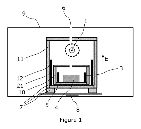
Figure 1 schematically illustrates the cross section of a device used to
implement the invention.
Generally, the term "microwaves" is understood to mean electromagnetic
waves the frequency of which is comprised between 300 MHz and 300 GHz. The
frequency of the microwaves 1 used in the invention is comprised between 900
MHz and 1000 MHz, so as to partially solve the problems of the prior art: the
microwave frequency chosen is among the lowest frequencies of the microwave-
frequency range so as to heat a solid part 4 made of ceramic material with the
largest possible penetration depth, and so as to obtain the largest possible
volume
able to heat a part uniformly in a microwave cavity. In particular, a single-
mode
resonant cavity, as schematically illustrated in figure 1, contains a volume
of 9 L
able to uniformly heat a sample when the frequency of the microwaves 1 is 915
MHz. The microwaves 1 are for example emitted into the cavity in a direction
normal to the plane of the cross section illustrated in figure 1. In
comparison, a
similar cavity, but modified (for example geometrically) to be single-mode
resonant for microwaves 1 of a frequency equal to 2.45 GHz would contain a
similar volume of 25 times smaller size. In the various embodiments of the
invention, the size of the solid part 4 made of ceramic material is chosen to
be
smaller than the size of the cavity. Advantageously, it is possible to choose
the
size of the solid part 4 depending, inter alia, on the frequency of the
emitted
microwaves 1: D being the maximum size of a part 4, it is possible to choose
the
size D so that the ratio between the penetration depth of the microwaves into
the
material of the part 4 and D is comprised between 0.5 and 100, and preferably
between 0.5 and 10. In the various embodiments of the invention, the
microwaves
1 may be emitted into a cavity 9 with a magnetron.
Generally, in all of the embodiments of the invention, the method is
carried out in a cavity 9 formed by a chamber the geometry of which is
suitable
for propagating and supporting single-mode (monomode) resonance of an
electromagnetic field at a frequency vo comprised between 900 MHz and 1 GHz,
and advantageously substantially equal to 915 MHz. In the various embodiments
of the invention, the configuration employed is preferably one in which the
cavity
9 is designed to support one mode of resonance of the microwaves 1 - the
cavity 9
is thus said to be single-mode. The geometry of the cavity 9 may be adjusted
CA 03041915 2019-04-26
8
before the introduction of a sample so as to be single-mode. The cavity
illustrated
in figure 1 is schematic: in practice, it is possible to modify the cavity by
varying,
for example, the parameters of a movable short-circuit piston or of an iris in
the
waveguides that are used to introduce the microwaves 1 into the cavity. In ah
l of
the embodiments of the invention, the electric field E in the cavity when it
is
empty, when the microwaves 1 are emitted into it, bas a uniform direction. In
particular, the direction of the field E is uniform in the volume in which a
solid
part 4 made of ceramic material is placed during a heat-treatment process and
advantageously a densification process. A vector E is illustrated in figure 1.
At least one solid part 4 made of ceramic material is placed in a cavity 9. It
is advantageously placed on a holder made of a thermal insulator 7. By "solid
part
made of ceramic material" what is meant is a part comprising at least one
ceramic
material and that is able to support itself mechanically, for example when
placed
on a holder, in contrast to a powder of ceramic material placed in a crucible.
A
solid part 4 made of ceramic material may be porous. By "porous" what is meant
is that a solid part 4 contains pores, i.e. volumes able to contain a liquid
or
gaseous medium. In particular, a porous material is a material having a ratio
between the volume of pores and the apparent volume of the material
substantially
different from zero, and preferably higher than 1%. The solid part 4 is able
to
support itself, when placed on a holder, by virtue for example of bonds
between
the various grains of the material, ensuring the mechanical stability of the
part.
Generally, the ceramic material of a solid part 4 made of ceramic material is
suitable for absorbing microwaves 1 at the frequency vo and at a temperature T
higher than or equal to 700 C. In particular embodiments of the invention, the
material of a solid part 4 may be a ceramic oxide, for example chosen from
alumina, zirconia and spinel. The mode of propagation of the microwaves 1
through the cavity 9 may be chosen so as to optimize the absorption of the
microwaves 1 by the material of the part 4. During the emission of the
microwaves 1, at least one stationary local electric-field and/or magnetic-
field
extremum may be formed in separate locations in a single-mode cavity 9. For
example anti-nodes and nodes of the electric and/or magnetic field may be
arranged longitudinally in a cavity 9 in phase quadrature. Preferably, a solid
part 4
made of ceramic material is arranged at an antinode of the electric or
magnetic
field in the cavity 9.
CA 03041915 2019-04-26
9
In one particular embodiment of the invention, the thermal insulator 7 may
for example be the thermal insulator 7 liteCell (AET Technologies, thermal
insulator with a high alumina content).
The solid part 4 made of ceramic material is surrounded by at least one
first susceptor 3. In one particular embodiment of the invention, which is
illustrated in figure 1, a solid part 4 made of ceramic material is surrounded
by
two first susceptors 3, to the left and to the right of the solid part 4 made
of
ceramic material, respectively. In other embodiments of the invention, one or
more first susceptors 3 may surround a solid part 4 made of ceramic material.
Advantageously, at least one element chosen from a ridge and an apex of at
least
one said first susceptor is rounded. This characteristic limits or prevents
the
appearance of plasma during the heat treatment. By "rounded" what is meant is
that the various walls of a first susceptor 3 join to form ridges and/or
apexes the
surface of which follows at least one radius of curvature the length of which
is
larger than one-thousandth of the maximum dimension of the cavity 9 and
preferably than one-hundredth of the maximum dimension of the cavity 9.
The dimensions, the material and the arrangement of the one or more first
susceptors 3 are chosen, or configured, so that infrared radiation is emitted
directly toward a said solid part 4 during an interaction with the microwaves
(1) at
the frequency vo in the vicinity of each said solid part 4 or around each said
part
4. By "directly", what is meant is that the path of the infrared radiation
emitted by
one or more first susceptors 3 toward the one or more solid parts 4 does not
pass
through any other part made of solid material and passes only through the gas
phase surrounding the one or more solid parts 4.
By "in the vicinity" what is meant is a length smaller than the
characteristic length of one or more than one solid part 4 made of ceramic
material.
A susceptor is a material capable of an excellent absorption of the
radiation of the microwaves 1 at a given frequency. During the absorption of
this
radiation, the susceptor material may re-emit the absorbed energy via infrared
radiation 2 for example. The absorption of a susceptor material is governed by
high dielectric, electric or magnetic losses during the excitation of the
material by
an electromagnetic field, as for example in the case of the microwaves I. The
CA 03041915 2019-04-26
materials used as first and/or second susceptors in the embodiments of the
invention may advantageously be silicon carbide (SiC) and/or lanthanum
chromite
(LaCr03). Other materials with high capacities to absorb microwaves 1 may be
used. Materials including a refractory and semiconductor oxide of a transition
5 metal may be
used. It is also possible to use materials composed of carbides, such
as boron carbide for example.
Generally, and in ail of the embodiments of the invention, the first
susceptors 3 comprise at least one first main surface 5. By "main surface"
what is
meant is that the arrangement of a portion or of the entirety of a first
susceptor 3
10 or of a second
susceptor 12 may be defined by a surface. A main surface may be a
plane: figure 1 for example illustrates two first susceptors 3 the first main
surfaces
5 of which are planes, said susceptors being seen in cross section. One of
these
main surfaces is illustrated by the dashed white une. A main surface may also
be
curved, for example in the case of the lateral surface of a cylinder.
Generally, and
in ah l of the embodiments of the invention, each said first or second main
surface
5, 21 of each said first or second susceptor 3, 12 is a ruled surface, the
generatrices of which are parallel to the electric field E of the cavity 9
when it is
empty, and/or of the volume suitable for receiving the sample. This feature
allows
one technical problem of the prior art to be solved, namely that of how to
treat a
solid part 4 made of ceramic material at high temperature, for example at a
temperature above 700 C, with microwaves 1 of frequency vo comprised between
900 MHz and 1 GHz, without forming a plasma or any electric arcs in the cavity
9. Physical aspects of the solution to this technical problem are detailed in
the
description of figures 6 and 7.
Local absorption of the microwaves 1 allows, depending on the
arrangement of the various susceptors in the cavity 9, a volume to be formed
in
which the solid part 4 may be heated directly by the one or more first
susceptors
3, by infrared radiation.
Advantageously, the assembly formed by a solid part 4 made of ceramic
material and the one or more first susceptors 3 surrounding a solid part 4
made of
ceramic material is arranged (or placed) in a first thermal confinement 10
made of
thermal insulator 7. In one particular embodiment of the invention, the
thermal
insulator 7 may be made of liteCell (AET Technologies S.A.S., thermal
insulator
with a high alumina content) and/or Quartzel (registered trademark, Saint-
Gobain
CA 03041915 2019-04-26
11
Quartz S.A.S.). This confinement by a thermal insulator 7 allows energy losses
via radiation during the heat treatment to be limited. The shape of the
thermal
confinement 10 may be cylindrical.
In one embodiment of the invention illustrated in figure 1, two second
susceptors 12 surround a first thermal confinement 10. The assembly composed
of
the second susceptors 12 and of the first thermal confinement 10 is surrounded
by
a second thermal confinement 11 made of thermal insulator 7. This structure
allows the thermal confinement to be increased. In this particular embodiment
of
the invention, the second thermal confinement 11 is made of a thermal
insulator 7.
In the embodiment of the invention illustrated in figure 1, the second
thermal confinement 11 is placed on a deck 8 made of aluminum.
The cavity 9, the first thermal confinement 10 and the second thermal
confinement 11 may be drilled in order to allow a pyrometric line of sight 6
to be
drawn. This line of sight 6 may allow a remote temperature sensor to measure
the
temperature of a solid part 4 made of ceramic material during a heat
treatment. In
one particular embodiment of the invention, the temperature sensor and the
emitter of the microwaves 1 are connected by way of a bus to a processing
unit.
The processing unit comprises one or more microprocessors and a memory. The
processing unit makes it possible to independently control the emission power
of
the microwave emitter and to process the information delivered by the
temperature
sensor. In particular embodiments of the invention, the power is automatically
controlled depending on a given temperature set point. The temperature set
point
may be variable over time so as to allow defined treatment temperature
profiles,
such as temperature ramps or constant-temperature heat treatments, to be
performed. According to one embodiment of the invention, it is possible to
measure, throughout or during some of the emission of the microwaves 1, the
temperature of a solid part 4 made of ceramic material, and then to adjust or
automatically control the emission power of the microwaves depending on the
measured temperature.
Figure 2 is a photograph of one portion of a device used to implement a
method of the invention. A solid part 4 made of ceramic material is
schematically
illustrated therein by a white rectangle, for the sake of clarity of the
photograph.
CA 03041915 2019-04-26
12
Two first susceptors 3 surround the solid part 4 made of ceramic material. By
"surround" what is meant here is that at least half of the area of a solid
part 4
made of ceramic material is located in the vicinity of a first susceptor 3.
The first
main surface 5 of one of the first susceptors 3 is shown by a dashed white
rectangle in perspective. The field E is illustrated at the bottom right of
the
photograph. In this embodiment of the invention, the planar first main
surfaces 5
of the two susceptors are parallel to the direction of the field E. The first
susceptors 3 and the solid part 4 made of ceramic material are placed in the
interior of a first thermal confinement 10, partially formed by the four
bricks
illustrated in the photograph.
Figure 3 is a schematic representation of a side view of the cavity 9
containing a part 4, and of the electric and magnetic fields associated with
varions
configurations of the cavity 9. A cavity 9 may be formed from walls, from a
coupling iris 19 at one of its ends and from a short-circuit piston 20 at the
other of
its ends. A first configuration (a) is associated with a position of a
coupling iris 19
and a position of a short-circuit piston 20, which positions are indicated by
irregular dot-dashed unes. A second configuration (b) is associated with
another
position of a coupling iris 19 and another position of a short-circuit piston
20,
which positions are also indicated by irregular dot-dashed unes. In the middle
of
figure 3, the amplitude of the electric field (c) and the amplitude of the
magnetic
field (d) corresponding to configuration (a) of the cavity are schematically
illustrated. At the bottom of figure 3, the amplitude of the electric field
(c) and the
amplitude of the magnetic field (d) corresponding to configuration (b) of the
cavity are schematically illustrated.
In the embodiments of the invention, the part 4 is placed at a local
extremum of the electric or magnetic field. In configuration (a) of the
cavity, the
part 4 is placed at an anti-node (or extremum) of the amplitude of the
magnetic
field (d) and at a node of the electric field (c). In configuration (b) of the
cavity,
the part 4 is placed at an anti-node (or extremum) of the electric field (c)
and at a
node of the magnetic field (d).
Figure 4 is a schematic representation of an indirect heating method
different from the invention. Panel A of figure 4 is a schematic
representation of a
top view of the implementation of an indirect heating operation.
CA 03041915 2019-04-26
13
Indirect heating requires at least one first susceptor 3 and a sample 18
surrounded by the one or more first susceptors 3. In the case of indirect
heating,
the material from which the sample 18 to be heated is made is transparent to
the
microwaves 1 or opaque to the microwaves 1.
By "transparent" what is meant is a material the dielectric and/or magnetic
losses of which are substantially zero when the material is subjected to a
microwave field 1 at a given frequency. A transparent material generally
possesses a very low electrical conductivity. The electrical conductivity of a
transparent material may be lower than 1O S.m1, preferably lower than 10-1
S.rn-1 and more preferably lower than 10-12 S.m-'.
By "opaque" what is meant is a material that reflects the radiation of the
microwaves 1 for a given frequency. An opaque material in general possesses a
high electrical conductivity. The electrical conductivity of an opaque
material is
preferably higher than 103 S.m-1. In this embodiment, which is different from
that
of the invention, the interaction between the microwaves 1 and the sample 18
does
flot allow the temperature of the sample 18 to increase. In contrast, the
susceptor 3
placed around the sample 18 absorbs the microwaves 1 and emits infrared
radiation 2. The sample may then be heated by the infrared radiation 2.
Panel B of figure 4 schematically illustrates a temperature profile along an
axis passing through the center of the sample 18. The two temperature maxima
of
this implementation are located at the distance (indicated by the abscissa d)
of the
location of the first susceptor 3. The temperature at the center of the sample
is
mainly due to heating by infrared radiation 2 of the periphery of the sample
and/or
convection of the medium surrounding the sample, coupled with thermal
conduction within the sample as explained above.
This mode of heat treatment does not allow one technical problem of the
prior art to be solved: a significant portion of the efficiency enabled by
heating
with the microwaves 1 is lost.
Figure 5 is a schematic representation of a direct heating method different
from the invention. Panel A of figure 5 is a schematic representation of a top
view
of the implementation of a direct heating operation. In the case of direct
heating,
the material from which the sample 18 to be heated is made absorbs the
. ,
CA 03041915 2019-04-26
14
microwaves 1 at a given frequency. The interaction between the microwaves 1
and
the absorbent material of the sample 18 allows the sample to be heated.
Panel B of figure 5 schematically illustrates a temperature profile along an
axis passing through the center of the sample 18. In this implementation,
which is
5 different from
the invention, the temperature profile has a maximum at the center
of the sample. The profile may be different because it in particular depends
on the
size of the sample 18, on the material of the sample 18, and on the power and
wavelength of the emitted microwaves 1.
This implementation does flot allow certain technical problems of the prior
10 art to be
solved. If the sample 18 is a solid part 4 made of ceramic material, it is
possible for the material of the part not to be able to be directly heated by
microwaves 1 at room temperature. In addition, a porous part 4 will be
densified
during a high-temperature heat treatment: in the case of certain ceramic
materials,
if the density of the part is too high, the penetration volume of the
microwaves 1
15 may be small
with respect to the total volume of the part 4. The effectiveness of
the heating achieved with the microwaves 1 is thus restricted, and does flot
allow
certain temperature set points, for example temperatures above 700 C, to be
reached.
Figure 6 is a schematic representation of a top view of a hybrid heating
20 process
according to one embodiment of the invention. The implementation of this
embodiment of the invention includes a solid part 4 made of ceramic material.
The
sample is surrounded by a first susceptor 3. In this embodiment of the
invention,
the susceptor 3 absorbs, at a given frequency, the microwaves 1. The first
susceptor 3 emits, in this case, infrared radiation 2 that contributes to the
heat
25 treatment of the solid part 4 made of ceramic material, in
particular during a first
phase of increase of the temperature of the solid part 4, in which phase the
material of the solid part 4 is able to interact only weakly with the
microwaves 1.
Furthermore, some of the microwaves 1 may be absorbed, at a given frequency,
by
the solid part 4 made of ceramic material. This hybrid process allows the
solid
30 part 4 to be heated via a contribution made by the infrared
radiation and via a
contribution made by the microwave radiation 1: the local strength of the
electromagnetic field may be moderate in comparison to when an equivalent part
4
is heated in the absence of a first susceptor 3, so as to limit the formation
of a
. .
CA 03041915 2019-04-26
plasma 14 in the vicinity of the solid part 4 made of ceramic material while
initiating an increase in the temperature of the solid part 4..
Figure 7 is an illustration of a simulation of the strength of the electric
5 field around
a susceptor different from a susceptor employed in the invention. The
strength of the electric field is illustrated by the greyscale of the
illustration, the
maximum strength of E corresponding to the color black. In this embodiment, a
first susceptor is a crucible, used for example to sinter a ceramic material
initially
in powder form. This first susceptor may also contain a solid part 4 made of
10 ceramic
material as illustrated in figure 7. The unes of the electric field E are
illustrated by thin black unes. In the absence of first susceptor and solid
part 4
made of ceramic material, the field unes are vertical. The geometry of the
illustrated crucible-shaped susceptor does not only comprise first main
surfaces 5
the generatrices of which are parallel to the electric field E of an empty
cavity 9.
15 The inventors
have discovered that the one or more first main surfaces 5 not
parallel to the electric field E of an empty cavity 9 are particularly likely
to lead
to spatial zones in which the electric field is of high-strength, and to
discontinuities in the electric field at the surface of a first and/or second
susceptor, during the emission of microwaves 1. These zones are particularly
likely to lead to the appearance of a plasma and/or electric arcs during the
heat
treatment and/or densification of a solid part 4 made of ceramic material. The
inventors have discovered that it is possible to decrease the size of these
zones by
employing only one or more first susceptors 3 the first main surfaces 5 of
which
are parallel to the direction of E in an empty cavity, i.e. susceptors each
said first
main surface 5 of which is a ruled surface the generatrices of which are
parallel to
E in an empty cavity 9. It is also possible to decrease the size of these
zones by
placing, in the cavity, one or more second susceptors 12 each said second main
surface 21 of which is a ruled surface the generatrices of which are parallel
to E in
an empty cavity 9.
Figure 8 is a set of illustrations of simulation of the strength of the
electric
field about a susceptor different from a susceptor employed in the invention.
The
strength of the electric field is illustrated by the greyscale of the
illustration, the
maximum strength of E corresponding to the color black.
= .
CA 03041915 2019-04-26
16
In partieular, panel A of figure 8 is a detail of figure 7, corresponding to
the bottom portion of the crucible, the geometry of which comprises no first
main
surface 5 parallel to E in an empty cavity. The dashed une corresponds to the
exterior surface of the susceptor, which is arranged above the dashed line.
The
strength, the variation in the strength and the discontinuity in the electric
field
illustrated in panel A may favor the appearance of a plasma and/or electric
arc
during the emission of microwaves 1.
Panel B of figure 8 is a detail of figure 7, corresponding to a portion on the
right of the crucible illustrated in figure 7. This portion comprises a first
main
surface parallel to the field E in an empty cavity. The average strength of E
is
lower than the average strength illustrated in panel A. The arrangement of
this
portion allows a temperature increase to be obtained that is sufficient for an
effective heat treatment and/or an effective densification without forming a
plasma and/or an electric arc in the cavity 9.
Figure 9 illustrates the variation in the temperature of a solid part 4 made
of ceramic material during a heat treatment according to one embodiment of the
invention. The ceramic material used may be alumina. In the embodiment of the
invention the variation of which is illustrated, the temperature set point is
1600 C.
This set point is achieved in less than 250 min. Three phases of the variation
may
be seen: a first phase (between 0 min and about 40 min) in which the slope of
the
variation is on average 9 C/min, a second phase (about between 40 min and 150
min) in which the slope of the variation is on average 6.5 C/min and a third
phase
(about between 150 min and 210 min) in which the slope of the variation is on
average 3.5 C. This variation has an influence on the microstructure of the
ceramic material of a part 4.
Figure 10 is a micrograph taken by scanning electron microscopy of a
cross section of a solid part 4 made of ceramic material after a heat
treatment
according to one embodiment of the invention. The ceramic material used may be
alumina. The scale bar corresponds to a length of 1 iim. The microstructure of
the
ceramic material of the micrograph corresponds to that obtained with the heat
treatment the variation of which is illustrated in figure 9. Initially, before
the heat
treatment, the employed solid part 4 made of ceramic material is a pellet of
the
CA 03041915 2019-04-26
17
oxide alumina, the diameter of which is for example 80 mm. After a
densification
process according to one embodiment of the invention, the measured density of
the solid part 4 made of ceramic material is strictly higher than 95% (by
volume)
and the microstructures observed in the material are fine: in particular,
figure 10
illustrates a microstructure the grains 17 of which have an average diameter
smaller than one micron and substantially equal to 350 nm. When the susceptors
comprise first main surfaces 5 and/or second main surfaces 21 that are flot
parallel
to the field E of an empty cavity 9, the appearance of a plasma may prevent
this
setpoint temperature from being reached. In embodiments of the invention, the
heat-treatment time corresponding to a step of emitting the microwaves 1, and
the
power of the emitted microwaves 1, may be parameterized so as to heat treat
and/or densify a solid part 4 made of ceramic material to a value higher than
90%
ceramic material per unit volume.
In embodiments of the invention, the ceramic material of a part 4 may be
polyphase, and comprise a plurality of different ceramic phases. The
properties of
interaction of these materials with the microwaves 1 may be different during
an
emission of microwaves 1 of frequency vo comprised between 900 MHz and 1
GHz. The arrangement of the various first susceptors 3 may allow the power
dissipated in the various phases to be varied and thus certain, or at least
one, of
the phases of one material of a part 4 to be selectively heat-treated and/or
densified.
Advantageously, two parts 4 made of optionally porous ceramics may be
heat treated so as to be brazed during the microwave emission. A process
according to the invention allows, in this case, conventional temperatures for
brazing ceramic parts to be reached while decreasing the risk of appearance of
a
plasma, while saving energy with respect to conventional brazing methods and
while decreasing the time required to reach these conventional brazing
temperatures (which may be comprised, depending on the ceramic material of a
solid part 4, for example between 600 C and 1200 C).