Note: Descriptions are shown in the official language in which they were submitted.
CA 03042224 2019-04-29
WO 2018/080992 PCT/US2017/057868
- 1 -
BACKLIGHT UNIT FOR A DISPLAY DEVICE
BACKGROUND OF THE INVENTION
Field
[0001] The present invention relates to display devices including light-
emitting diode
(LEDs) based backlight units (BLUs) and phosphor films including luminescent
nanostructures such as quantum dots (QDs).
Background
[0002] Display devices (e.g., liquid crystal displays (LCDs)) are used as
screens or
displays for a wide variety of electronic devices and typically require some
form of
backlighting for images to be visible in normal or reduced ambient light
environments. In
a BLU of the display device, LEDs are typically utilized as a light source.
The LEDs may
be arranged in a two dimensional array behind the viewing area of the display
device or
around the edge or perimeter of the display device. The BLU may also utilize
phosphors,
such as yttrium-aluminum-garnet (YAG) phosphors.
[0003] Luminescent nanostructures represent a class of phosphors often
used in
configurations where the phosphor may be placed external to the LEDs. Light
emanating
from the LEDs may be processed through a phosphor film of the display device
to
produce white light, which may be distributed across a display screen of the
display
device.
[0004] For example, luminescent nanostructures may be embedded in a
flexible
film/sheet (e.g., quantum dot enhancement film (QDEFg) supplied commercially
from
3M Company, St. Paul, Minnesota using quantum dots supplied by Nanosys, Inc,
Milpitas, California) that may be placed in the display device (see, e.g.,
U.S. Patent
Publication Nos. 2010/0110728 and 2012/0113672, which are incorporated by
reference
herein in their entirety). QDEF is a registered trademark of Nanosys, Inc.
[0005] One of the factors used to define the image quality of a display
device is the color
gamut coverage of standard RGB color spaces such as Rec. 2020, Rec. 709, DCI
P3,
NTSC, or sRGB provided by the display device. FIG. 1 illustrates a definition
of color
CA 03042224 2019-04-29
WO 2018/080992 PCT/US2017/057868
- 2 -
gamut coverage of a display device. In FIG. 1, area 101 formed between 1976
CIE color
coordinates 101a-101c represents the color gamut of a standard RGB color space
(e.g.,
Rec. 2020) on the 1976 CIE u'-v' chromaticity diagram 100. Area 102 formed
between
1976 CIE color coordinates 102a-102c represents the color gamut of the display
device
on the 1976 CIE u'-v' chromaticity diagram 100. Color gamut coverage of the
display
device may be defined as a ratio of the overlapping area 103 between areas 101
and 102
to area 101. The wider the color gamut coverage of a display device allows the
display
device to render a wider range of colors identifiable by the human eye (i.e.,
the visible
spectrum), and hence, improves the image quality of the display device
assuming the
other factors contributing to the image quality are optimized.
[0006] Current display devices suffer from a trade-off between achieving
the desired
brightness (e.g., brightness required by high dynamic range (HDR) imaging
standards)
and the desired color gamut coverage (e.g., greater than 85%) of the standard
RGB color
spaces. For example, some display devices suffer about 30% loss in brightness
to achieve
over 90% DCI P3 color gamut coverage. Hence, with current technology, loss of
brightness in display devices would be significantly higher in order to
achieve color
gamut coverage of color spaces that are even wider than DCI P3 (e.g., Rec.
2020).
SUMMARY
[0007] Accordingly, there is need for display devices with less of a trade-
off between
achieving the desired color gamut coverage of the wide RGB color spaces and
the desired
brightness.
[0008] According to an embodiment, a backlight unit (BLU) of a display
device includes
a light source, a quantum dot film, and a radiation absorbing element. The
quantum dot
film is optically coupled to the light source and is configured to process
light received
from the light source. The radiation absorbing element is optically coupled to
the
quantum dot film and is configured to tune a spectral emission width of the
processed
light received from the quantum dot film to achieve over 90% color gamut
coverage of a
standard RGB color space.
[0009] According to another embodiment, a display device includes a
backlight unit
(BLU) and an image generating unit (IGU). The BLU includes an optical cavity
having a
top side, a bottom side, and side walls, and an array of light sources coupled
to the optical
CA 03042224 2019-04-29
WO 2018/080992 PCT/US2017/057868
- 3 -
cavity. The BLU further includes a quantum dot film that is positioned within
the optical
cavity and is configured to process light received from the array of light
sources. Further
included in the BLU is a radiation absorbing element that is positioned within
the optical
cavity and is configured to tune a spectral emission width of the processed
light received
from the quantum dot film to achieve over 90% color gamut coverage of the Rec.
2020
color space. The BLU is configured to transmit the tuned light to the IGU.
[0010] Further features and advantages of the invention, as well as the
structure and
operation of various embodiments of the invention, are described in detail
below with
reference to the accompanying drawings. It is noted that the invention is not
limited to the
specific embodiments described herein. Such embodiments are presented herein
for
illustrative purposes only. Additional embodiments will be apparent to persons
skilled in
the relevant art(s) based on the teachings contained herein.
BRIEF DESCRIPTION OF THE DRAWGINS/FIGURES
[0011] The accompanying drawings, which are incorporated herein and form
part of the
specification, illustrate the present embodiments and, together with the
description,
further serve to explain the principles of the present embodiments and to
enable a person
skilled in the relevant art(s) to make and use the present embodiments.
[0012] FIG. 1 is a CIE 1976 u'v' chromaticity diagram of Rec. 2020 color
gamut and a
color gamut of a display device.
[0013] FIGs. 2-3 are exploded cross-sectional views of backlit display
devices, according
to various embodiments.
[0014] FIG. 4 is a schematic of a cross-sectional view of a light source
unit of a backlit
display device, according to an embodiment.
[0015] FIG. 5 is schematic of a cross-sectional view of an edge-lit
display device,
according to an embodiment.
[0016] FIG. 6 is a schematic of a cross-sectional view of a barrier layer
coated QD,
according to an embodiment.
[0017] FIG. 7 is a schematic of a barrier layer coated QD film, according
to an
embodiment.
[0018] The features and advantages of the present invention will become
more apparent
from the detailed description set forth below when taken in conjunction with
the
CA 03042224 2019-04-29
WO 2018/080992 PCT/US2017/057868
- 4 -
drawings, in which like reference characters identify corresponding elements
throughout.
In the drawings, like reference numbers generally indicate identical,
functionally similar,
and/or structurally similar elements. The drawing in which an element first
appears is
indicated by the leftmost digit(s) in the corresponding reference number.
Unless
otherwise indicated, the drawings provided throughout the disclosure should
not be
interpreted as to-scale drawings.
DETAILED DESCRIPTION OF THE INVENTION
[0019] Although specific configurations and arrangements may be discussed,
it should be
understood that this is done for illustrative purposes only. A person skilled
in the
pertinent art will recognize that other configurations and arrangements can be
used
without departing from the spirit and scope of the present invention. It will
be apparent to
a person skilled in the pertinent art that this invention can also be employed
in a variety of
other applications beyond those specifically mentioned herein. It should be
appreciated
that the particular implementations shown and described herein are examples
and are not
intended to otherwise limit the scope of the application in any way.
[0020] It is noted that references in the specification to "one
embodiment," "an
embodiment," "an example embodiment," etc., indicate that the embodiment
described
may include a particular feature, structure, or characteristic, but every
embodiment may
not necessarily include the particular feature, structure, or characteristic.
Moreover, such
phrases do not necessarily refer to the same embodiment. Further, when a
particular
feature, structure or characteristic is described in connection with an
embodiment, it
would be within the knowledge of one skilled in the art to effect such
feature, structure or
characteristic in connection with other embodiments whether or not explicitly
described.
[0021] All numbers in this description indicating amounts, ratios of
materials, physical
properties of materials, and/or use are to be understood as modified by the
word "about,"
except as otherwise explicitly indicated.
[0022] In embodiments, the term "display device" refers to an arrangement
of elements
that allow for the visible representation of data on a display screen.
Suitable display
screens may include various flat, curved or otherwise-shaped screens, films,
sheets or
other structures for displaying information visually to a user. Display
devices described
herein may be included in, for example, display systems encompassing a liquid
crystal
CA 03042224 2019-04-29
WO 2018/080992 PCT/US2017/057868
- 5 -
display (LCD), televisions, computers, mobile phones, smart phones, personal
digital
assistants (PDAs), gaming devices, electronic reading devices, digital
cameras, tablets,
wearable devices, car navigation systems, and the like.
[0023] The term "about" as used herein indicates the value of a given
quantity varies by
10% of the value. For example, "about 100 nm" encompasses a range of sizes
from 90
nm to 110 nm, inclusive.
[0024] In embodiments, the term "forming a reaction mixture" or "forming a
mixture"
refers to combining at least two components in a container under conditions
suitable for
the components to react with one another and form a third component.
[0025] In embodiment, the terms "light guide plate," "light guide," and
"light guide
panel" are used interchangeably and refer to an optical component that is
suitable for
directing electromagnetic radiation (light) from one position to another.
[0026] In embodiments, the term "optically coupled" means that components
are
positioned such that light is able to pass from one component to another
component
without substantial interference.
[0027] The term "nanostructure" as used herein refers to a structure
having at least one
region or characteristic dimension with a dimension of less than about 500 nm.
In some
embodiments, the nanostructure has a dimension of less than about 200 nm, less
than
about 100 nm, less than about 50 nm, less than about 20 nm, or less than about
10 nm.
Typically, the region or characteristic dimension will be along the smallest
axis of the
structure. Examples of such structures include nanowires, nanorods, nanotubes,
branched
nanostructures, nanotetrapods, tripods, bipods, nanocrystals, nanodots, QDs,
nanoparticles, and the like. Nanostructures can be, e.g., substantially
crystalline,
substantially monocrystalline, polycrystalline, amorphous, or a combination
thereof In
some embodiments, each of the three dimensions of the nanostructure has a
dimension of
less than about 500 nm, less than about 200 nm, less than about 100 nm, less
than about
50 nm, less than about 20 nm, or less than about 10 nm.
[0028] The term "QD" or "nanocrystal" as used herein refers to
nanostructures that are
substantially monocrystalline. A nanocrystal has at least one region or
characteristic
dimension with a dimension of less than about 500 nm, and down to the order of
less than
about 1 nm. The terms "nanocrystal," "QD," "nanodot," and "dot," are readily
understood
by the ordinarily skilled artisan to represent like structures and are used
herein
CA 03042224 2019-04-29
WO 2018/080992 PCT/US2017/057868
- 6 -
interchangeably. The present invention also encompasses the use of
polycrystalline or
amorphous nanocrystals.
[0029] The term "heterostructure" when used with reference to
nanostructures refers to
nanostructures characterized by at least two different and/or distinguishable
material
types. Typically, one region of the nanostructure comprises a first material
type, while a
second region of the nanostructure comprises a second material type. In
certain
embodiments, the nanostructure comprises a core of a first material and at
least one shell
of a second (or third etc.) material, where the different material types are
distributed
radially about the long axis of a nanowire, a long axis of an arm of a
branched nanowire,
or the center of a nanocrystal, for example. A shell can but need not
completely cover the
adjacent materials to be considered a shell or for the nanostructure to be
considered a
heterostructure; for example, a nanocrystal characterized by a core of one
material
covered with small islands of a second material is a heterostructure. In other
embodiments, the different material types are distributed at different
locations within the
nanostructure; e.g., along the major (long) axis of a nanowire or along a long
axis of arm
of a branched nanowire. Different regions within a heterostructure can
comprise entirely
different materials, or the different regions can comprise a base material
(e.g., silicon)
having different dopants or different concentrations of the same dopant.
[0030] As used herein, the term "diameter" of a nanostructure refers to
the diameter of a
cross-section normal to a first axis of the nanostructure, where the first
axis has the
greatest difference in length with respect to the second and third axes (the
second and
third axes are the two axes whose lengths most nearly equal each other). The
first axis is
not necessarily the longest axis of the nanostructure; e.g., for a disk-shaped
nanostructure,
the cross-section would be a substantially circular cross-section normal to
the short
longitudinal axis of the disk. Where the cross-section is not circular, the
diameter is the
average of the major and minor axes of that cross-section. For an elongated or
high aspect
ratio nanostructure, such as a nanowire, the diameter is measured across a
cross-section
perpendicular to the longest axis of the nanowire. For a spherical
nanostructure, the
diameter is measured from one side to the other through the center of the
sphere.
[0031] The terms "crystalline" or "substantially crystalline," when used
with respect to
nanostructures, refer to the fact that the nanostructures typically exhibit
long-range
ordering across one or more dimensions of the structure. It will be understood
by one of
CA 03042224 2019-04-29
WO 2018/080992 PCT/US2017/057868
- 7 -
skill in the art that the term "long range ordering" will depend on the
absolute size of the
specific nanostructures, as ordering for a single crystal cannot extend beyond
the
boundaries of the crystal. In this case, "long-range ordering" will mean
substantial order
across at least the majority of the dimension of the nanostructure. In some
instances, a
nanostructure can bear an oxide or other coating, or can be comprised of a
core and at
least one shell. In such instances it will be appreciated that the oxide,
shell(s), or other
coating can but need not exhibit such ordering (e.g. it can be amorphous,
polycrystalline,
or otherwise). In such instances, the phrase "crystalline," "substantially
crystalline,"
"substantially monocrystalline," or "monocrystalline" refers to the central
core of the
nanostructure (excluding the coating layers or shells). The terms
"crystalline" or
"substantially crystalline" as used herein are intended to also encompass
structures
comprising various defects, stacking faults, atomic substitutions, and the
like, as long as
the structure exhibits substantial long range ordering (e.g., order over at
least about 80%
of the length of at least one axis of the nanostructure or its core). In
addition, it will be
appreciated that the interface between a core and the outside of a
nanostructure or
between a core and an adjacent shell or between a shell and a second adjacent
shell may
contain non-crystalline regions and may even be amorphous. This does not
prevent the
nanostructure from being crystalline or substantially crystalline as defined
herein.
[0032] The term "monocrystalline" when used with respect to a
nanostructure indicates
that the nanostructure is substantially crystalline and comprises
substantially a single
crystal. When used with respect to a nanostructure heterostructure comprising
a core and
one or more shells, "monocrystalline" indicates that the core is substantially
crystalline
and comprises substantially a single crystal.
[0033] The term "ligand" as used herein refers to a molecule capable of
interacting
(whether weakly or strongly) with one or more faces of a nanostructure, e.g.,
through
covalent, ionic, van der Waals, or other molecular interactions with the
surface of the
nanostructure.
[0034] The term "quantum yield" (QY) as used herein refers to the ratio of
photons
emitted to photons absorbed, e.g., by a nanostructure or population of
nanostructures. As
known in the art, quantum yield is typically determined by a comparative
method using
well-characterized standard samples with known quantum yield values.
CA 03042224 2019-04-29
WO 2018/080992 PCT/US2017/057868
-8-
100351 The term "primary emission peak wavelength" as used herein refers
to the
wavelength at which the emission spectrum exhibits the highest intensity.
[0036] The term "full width at half-maximum" (FWHM) as used herein refers
to refers to
a measure of spectral width. In the case of an emission spectrum, a FWHM can
refer to a
width of the emission spectrum at half of a peak intensity value.
[0037] The term Forster radius used herein is also referred as Forster
distance in the art.
[0038] The terms "luminance" and "brightness" are used herein
interchangeably and refer
to a photometric measure of a luminous intensity per unit area of a light
source or an
illuminated surface.
[0039] The terms "specular reflectors," "specularly reflective surfaces,"
and "reflective
surfaces" are used herein to refer to elements, materials, and/or surfaces
capable of
specular reflection.
[0040] The term "specular reflection" is used herein to refer to a mirror-
like reflection of
light (or of other kinds of wave) from a surface, when an incident light hits
the surface.
[0041] The published patents, patent applications, websites, company
names, and
scientific literature referred to herein are hereby incorporated by reference
in their entirety
to the same extent as if each was specifically and individually indicated to
be
incorporated by reference. Any conflict between any reference cited herein and
the
specific teachings of this specification shall be resolved in favor of the
latter. Likewise,
any conflict between an art-understood definition of a word or phrase and a
definition of
the word or phrase as specifically taught in this specification shall be
resolved in favor of
the latter.
[0042] Technical and scientific terms used herein have the meaning
commonly
understood by one of skill in the art to which the present application
pertains, unless
otherwise defined. Reference is made herein to various methodologies and
materials
known to those of skill in the art.
Overview
[0043] This disclosure provides various embodiments of QD-based BLUs of
display
devices that help to improve or eliminate the current existing trade-off
between achieving
the desired brightness and the desired color gamut in display devices.
CA 03042224 2019-04-29
WO 2018/080992 PCT/US2017/057868
- 9 -
Example Embodiments of a Backlit Display Device with Radiation Absorbing
Element
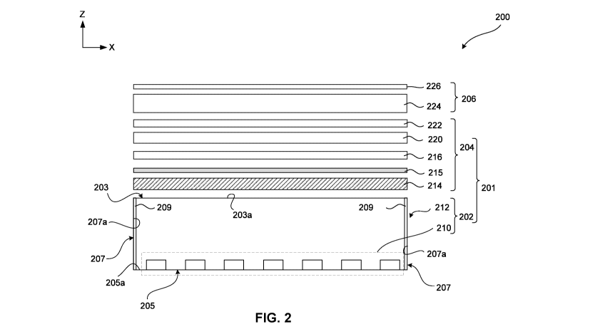
[0044] FIG. 2 illustrates a schematic of an exploded cross-sectional view
of a backlit
display device 200, according to an embodiment. Display device 200 may include
a BLU
201 having a light source unit (LSU) 202, an optical processing unit (OPU)
204, and an
image generating unit (IGU) 206.
[0045] LSU 202 may include an optical cavity 212 and an array of LEDs 210
(e.g., white
LEDs or blue LEDs) coupled to optical cavity 212. Optical cavity 212 may
include a top
side 203, a bottom side 205, sidewalls 207 and a closed volume confined by top
side 203,
bottom side 205, and sidewalls 207. LEDs 210 may be coupled to a top surface
205a of
bottom side 205 within the closed volume. LEDs 210 may be configured to
provide a
primary light (e.g., a blue light or a white light) that may be processed
through OPU 204
and subsequently, transmitted to IGU 206 to be distributed across a display
screen 226 of
IGU 206. In some embodiments, LEDs 210 may comprise blue LEDs that emit in the
range from about 440 nm to about 470 nm. In some embodiments, LEDs 210 may
comprise white LEDs that emit in the range from about 440 nm to about 700 nm
or other
possible light wavelength ranges. In an embodiment, the array of LEDs 210 may
comprise a two-dimensional array of LEDs that are spread across an area of top
surface
205a and the area may be equal to the surface area of display screen 226.
[0046] It should be noted that even though two sidewalls 207 are shown in
FIG. 2, a
person skilled in the art would understand that optical cavity 212 may include
any number
of sidewalls 207, according to various embodiments. For example, optical
cavity 212 may
have a cuboid shape and may include four sidewalls similar to sidewalls 207.
Optical
cavity 212 is not restricted to being cuboid in shape or having other straight-
sided shapes.
Optical cavity 212 may be configured to be any type of geometric shape, such
as but not
limited to cylindrical, trapezoidal, spherical, or elliptical, according to
various
embodiments, without departing from the spirit and scope of the present
invention. It
should also be noted that the rectangular cross-sectional shape of optical
cavity 212, as
illustrated in FIG. 2, is for illustrative purposes, and is not limiting.
Optical cavity 212
may have other cross-sectional shapes (e.g., trapezoid, oblong, rhomboid),
according to
various embodiments, without departing from the spirit and scope of the
present
invention.
CA 03042224 2019-04-29
WO 2018/080992 PCT/US2017/057868
- 10 -
[0047] Top side 203 of optical cavity 212 may be configured to be an
optically diffusive
and transmissive layer such that light from LEDs 210 may exit optical cavity
212 through
top side 203 with a substantially uniform distribution of brightness across
top surface
203a of top side 203 and traverse through OPU 204 and/or IGU 206. In an
embodiment,
top side 203 may include optically transparent areas and optically translucent
areas that
are strategically arranged over LEDs 210 to provide the substantially uniform
distribution
in light brightness exiting top side 203. In another embodiment, top side 203
may include
pores of varying sizes in diameters and optically translucent areas that are
strategically
arranged to provide the substantially uniform distribution in light brightness
exiting top
side 203.
[0048] Bottom side 205 and/or sidewalls 207 may be constructed from one or
more
materials (e.g., metals, non-metals, and/or alloys) that are configured to
have specularly
reflective top surface 205a and/or specularly reflective side wall interior
surfaces 207a,
respectively. For example, top surface 205a and/or side wall interior surfaces
207a may
be mirror-like surfaces having mirror-like reflection properties. In some
embodiments,
top surface 205a and/or side wall interior surfaces 207a may be completely
specularly
reflective or partially specularly reflective and partially scattering.
[0049] Optionally, optical cavity 212 may include specular reflectors 209
coupled to
sidewall interior surfaces 207a. Specular reflectors 209 may be coupled to
sidewall
interior surfaces 207a using optically transparent adhesive. The optically
transparent
adhesive may comprise tape, various glues, polymeric compositions such as
silicones, etc.
Additional optically transparent adhesive may include various polymers,
including, but
not limited to, poly(vinyl butyral), poly(vinyl acetate), epoxies, and
urethanes; silicone
and derivatives of silicone, including, but not limited to,
polyphenylmethylsiloxane,
polyphenylalkylsiloxane, polydiphenylsiloxane, polydialkylsiloxane,
fluorinated silicones
and vinyl and hydride substituted silicones; acrylic polymers and copolymers
formed
from monomers including, but not limited to, methylmethacrylate,
butylmethacrylate, and
laurylmethacrylate; styrene based polymers; and polymers that are cross linked
with
difunctional monomers, such as divinylbenzene, according to various examples.
[0050] Specularly reflective top surface 205a and side wall interior
surfaces 207a and
specular reflectors 209 may substantially minimize absorption of light from
LEDs 210
CA 03042224 2019-04-29
WO 2018/080992 PCT/US2017/057868
- 11 -
through bottom side 205 and/or side walls 207 and thus, substantially minimize
loss of
luminance within optical cavity 212 and increase light output efficiency of
LSU 202.
[0051] OPU 204 may be configured to process the light received from LSU
202 to a
desired characteristics for transmission to IGU 206. OPU 204 may include, but
not
limited to, a phosphor film 214, such as the QDEF film mentioned above, a
radiation
absorbing element 215, a brightness enhancing film (BEF) 216, a diffuser 220,
and a
reflective polarizing film (RPF) 222. It should be noted that OPU 204 may
include more
than one diffuser, BEF, and/or RPF without departing from the spirit and scope
of the
invention, as would be understood by a skilled person in the art.
[0052] Phosphor film 214 may be a QDEF including luminescent
nanostructures such as
QDs (e.g., QD 600 described with reference to FIG. 6). In an example
embodiment,
phosphor film 214 may include a plurality of luminescent nanostructures that
emit at the
same wavelength, for example, at the wavelength corresponding to green light
or red light
in the visible spectrum. In another example embodiment, phosphor film 214 may
include
a first plurality of luminescent nanostructures that emit at a first
wavelength (e.g.,
wavelength corresponding to green light) and a second plurality of luminescent
nanostructures that emit at a second wavelength (e.g., wavelength
corresponding to red
light) that is different from the first wavelength.
[0053] Phosphor film 214 may be a down-converter, where at least a portion
of the
primary light from optical cavity 212 may be absorbed, for example, by
luminescent
nanostructures in phosphor film 214 and re-emitted as secondary light having a
lower
energy or longer wavelength than the primary light. For example, the first
plurality of
luminescent nanostructures and the second plurality of luminescent
nanostructures may
absorb a portion of the blue light from optical cavity 212 and be excited to
emit green and
red secondary lights, respectively. The unabsorbed portion of the blue primary
light and
the green and red secondary lights may be mixed at a predetermined ratio to
produce
white light having a desired white point value to be transmitted through IGU
206 and
distributed across display screen 226 to serve as a backlight of display
device 200.
[0054] Radiation absorbing element 215 may be configured to tune the
spectral emission
widths (also referred as width of emission spectrum) of any processed and/or
unprocessed
light passing through radiation absorbing element 215 in order to achieve a
desired color
gamut coverage of display device 200. The term "processed light" as used
herein refers to
CA 03042224 2019-04-29
WO 2018/080992 PCT/US2017/057868
- 12 -
any light emitted from phosphor film 214 and the term "unprocessed light" as
used herein
refers to any light emitted from LSU 202 that may bypass phosphor film 214 to
reach any
of the layers/structures overlying phosphor film 214. In some embodiments,
radiation
absorbing element 215 may be configured to selectively tune the spectral
emission widths
of light emitted from the first or second plurality of luminescent
nanostructures in
phosphor film 214 or the unprocessed light from LEDs 210 (e.g., blue light).
In some
embodiments, radiation absorbing element 215 may be configured to tune the
spectral
emission widths of light emitted from both the first and second plurality of
luminescent
nanostructures in phosphor film 214. In some embodiments, radiation absorbing
element
215 may be configured to tune the spectral emission widths of light emitted
from both the
first and second plurality of luminescent nanostructures in phosphor film 214
and from
the unprocessed light from LEDs 210.
[0055] Tuning of the spectral emission widths may require absorbing one or
more
wavelengths from the processed and/or unprocessed light to narrow their
spectral
emission widths to achieve the desired color gamut coverage without
significant decrease
in brightness. For example, there may be less than 10% (e.g., about 8%, about
5%, about
3%, or about 1%) decrease in brightness due to this tuning process compared to
display
devices without radiation absorbing element 215. As processed light from
phosphor film
214 having QDs typically exhibit narrow spectral emission widths, the tuning
process
may not require absorption of wide range of wavelengths to achieve the desired
color
gamut coverage as required in current non-QD based display devices to achieve
similar
color gamut coverage.
[0056] Wide spectral emission width is one of the limitations in current
non-QD based
display devices (e.g., OLED based display devices, YAG-phosphor based display
devices) in achieving wide color gamut coverage of, for example, the Rec. 2020
color
space. Use of absorbing elements in current non-QD based display devices may
achieve
wide color gamut coverage (e.g., 80-90% Rec. 2020 color gamut coverage), but
at the
cost of significant decrease in brightness. Such decrease in brightness may
not only
adversely affect the image quality of the current display devices, but also
fail to meet the
brightness level required under the HDR imaging standards.
[0057] Radiation absorbing element 215 may include one or more non-
phosphor based
materials. That is, the one or more non-phosphor based materials exhibit
optical
CA 03042224 2019-04-29
WO 2018/080992 PCT/US2017/057868
- 13 -
absorption properties, but do not exhibit any optical emission properties. The
one or more
non-phosphor base materials may be selected based on their optical absorption
properties
to absorb only the one or more wavelengths or range of wavelengths that
require
absorbing during the above described tuning process. In some embodiments, the
one or
more non-phosphor materials may include the same absorption property. In some
embodiment, each of the one or more non-phosphor materials includes an
absorption
property different from each other.
[0058] The one or more non-phosphor materials may be selected such that
they may be
inexpensively disposed on phosphor film 214 or any other layer/structure of
display
device 200 to form radiation absorbing element 215. For example, the one or
more non-
phosphor materials may be dye (e.g., narrow band organic Exciton P491 dye),
ink, paint,
polymeric material, an/or any material that may be sprayed, painted, spin-
coated, printed,
or any other suitable low temperature (e.g., below 100 C) deposition method.
Printing
may be done using, for example, a plotter, an inkjet printer, or a screen
printer. In some
embodiments, the one or more non-phosphor materials may be directly disposed
on
phosphor film 214. In some embodiments, radiation absorbing element 215 may
include a
substrate having the one or more non-phosphor materials disposed on it.
[0059] The placement of radiation absorbing element 215 shown in FIG. 2 is
not limiting.
It may be placed above or below phosphor film 214. It may be placed below
phosphor
film 214 and on top surface 203 of optical cavity 212. It may be placed on any
layers/structures of BLU 201. For example, radiation absorbing element 215 may
be
placed on BEF 216 or diffuser 220.
[0060] In some embodiments, radiation absorbing element 215 may not be a
separate
structure as shown in FIG. 2, but may be included in any layers/structures of
BLU 201.
For example, radiation absorbing element 215 may be a part of phosphor film
214. That
is, phosphor film 214 may be a composite film comprising the luminescent
nanostructures, as described above, along with radiation absorbing element
215. The one
or more non-phosphor materials of radiation absorbing element 215 such as dye,
ink,
paint, polymeric material, or a combination thereof may be incorporated or
embedded in a
matrix of phosphor film 214. The one or more non-phosphor materials may
include
nanostructured materials that may be dispersed in a matrix of phosphor film
214. These
nanostructured materials may exhibit optical absorption properties and may not
exhibit
CA 03042224 2019-04-29
WO 2018/080992 PCT/US2017/057868
- 14 -
any optical emission properties. In some embodiments, radiation absorbing
element 215
may be included in BEF 216 or diffuser 220. For example, the one or more non-
phosphor
materials of radiation absorbing element 215 discussed above may be
incorporated in the
structure of BEF 216 or diffuser 220 described below.
[0061] BEF 216 may include reflective and/or refractive films, reflective
polarizer films,
prism films, groove films, grooved prism films, prisms, pitches, grooves, or
any suitable
BEFs or brightness enhancement features known in the art. For example, BEF 216
may
include conventional BEF such as VikuitiTM or BEF available from 3MTm.
According to
various embodiments, OPU 204 may include at least one BEF, at least two BEFs,
or at
least three BEFs. In example embodiments, at least one BEF comprises a
reflective
polarizer BEF, e.g., for recycling light which would otherwise be absorbed by
RPF 222.
The brightness-enhancing features and BEF 216 may include reflectors and/or
refractors,
polarizers, reflective polarizers, light extraction features, light recycling
features, or any
brightness-enhancing features known in the art. BEF 216 may include a first
layer having
pitches or prisms having a first pitch angle, according to an embodiment.
Additionally or
optionally, another BEF (not shown) in OPU 204 may include a second layer
having
pitches or prisms having a second pitch angle that is different from the first
pitch angle.
[0062] The brightness-enhancing features of BEF 216 may be configured to
reflect a
portion of the primary light (e.g., blue light from optical cavity 212) back
toward
phosphor film 214, thereby providing recycling of the primary light back into
phosphor
film 214. Because of light recycling, portions of the primary light may pass
through
phosphor film 214 multiple times before exiting BLU 201. Light transmitted
through BEF
216 may be dependent on the angle at which the light is incident upon BEF 216.
For
example, light traveling upward from optical cavity 212 may transmit through
BEF 216 if
the light is normal or perpendicular to BEF 216. However, such light may be
reflected
downward toward optical cavity 212 if the light has a higher angle. BEF 216
may be
selected to have multiple reflection angles for light of different angles to
achieve a desired
recycling of the primary light. Such recycling of the primary light may
increase optical
path length of the primary light in phosphor film 214, resulting in increased
absorption of
the primary light and increased re-emission of one or more secondary lights,
such as but
not limited to green light or red light.
CA 03042224 2019-04-29
WO 2018/080992 PCT/US2017/057868
- 15 -
[0063] Diffuser 220 is distinct from and supplemental to the scattering
features described
herein. According to an example of this embodiment, diffuser 220 may include
any
diffuser film known in the art, including gain diffuser films, and may be
disposed above
or below BEF 216 or other optical films of display device 200. In example
embodiments,
phosphor film 214 may eliminate the need for a conventional bottom diffuser
(not
shown), thereby minimizing the thickness of BLU 201. The compositions of
phosphor
film 214 may also include one or more scattering or diffuser features
associated
therewith, which may serve the purpose of traditional diffusers in addition to
increasing
secondary emission of luminescent nanostructures in phosphor film 214.
[0064] IGU 206 may include an LCD module 224 and display screen 226 and
may be
configured to generate images on display screen 226. Display screen 226 may be
a touch
screen display, according to an example embodiment. In some embodiments,
radiation
absorbing element 215 may be placed on or within any layers/structures of IGU
206. For
example, radiation absorbing element 215 may be placed on or within LCD module
224.
[0065] Display device 200 may further comprise one or more medium
materials (not
shown) disposed between any of the adjacent elements in display device 200,
for example
between optical cavity 212 and phosphor film 214; between radiation absorbing
element
215; between phosphor film 214 and BEF 216, diffuser 220, RPF 222, or other
features;
or between any other elements of display device 200. The one or more medium
materials
may include, but not limited to, a vacuum, air, gas, optical materials,
adhesives, optical
adhesives, glass, polymers, solids, liquids, gels, cured materials, optical
coupling
materials, index-matching or index-mismatching materials, index-gradient
materials,
cladding or anti-cladding materials, spacers, epoxy, silica gel, silicones,
brightness-
enhancing materials, scattering or diffuser materials, reflective or anti-
reflective
materials, wavelength-selective materials, wavelength-selective anti-
reflective materials,
color filters, or other suitable medium material known in the art. Medium
materials may
also include optically transparent, non-yellowing, pressure-sensitive optical
adhesives.
Suitable materials include silicones, silicone gels, silica gel, epoxies
(e.g., LoctiteTM
Epoxy E-30CL), acrylates (e.g., 3MTm Adhesive 2175). The one or more medium
materials may be applied as a curable gel or liquid and cured during or after
deposition, or
pre-formed and pre-cured prior to deposition. Curing methods may include UV
curing,
thermal curing, chemical curing, or other suitable curing methods known in the
art. Index-
CA 03042224 2019-04-29
WO 2018/080992 PCT/US2017/057868
- 16 -
matching medium materials may be chosen to minimize optical losses between
elements
of BLU 201.
[0066] Display device 200 may be any type of geometric shape, such as but
not limited to
cylindrical, trapezoidal, spherical, or elliptical, according to various
embodiments,
without departing from the spirit and scope of the present invention. Display
device 200
is not restricted to being cuboid in shape or having other straight-sided
shapes. It should
be noted that the rectangular cross-sectional shape of display device 200 is
for illustrative
purposes, and is not limiting. Display device 200 may have other cross-
sectional shapes
(e.g., trapezoid, oblong, rhomboid), according to various embodiments, without
departing
from the spirit and scope of the present invention. It should also be noted
that even
though optical cavity 212, phosphor film 214, radiation absorbing element 215,
BEF 216,
diffuser 220, RPF 222, LCD module 224, and display screen 226 are shown in
FIG. 2 to
have similar dimensions along X direction, a person skilled in the art would
understand
that each of these components may have dimensions different from each other in
one or
more directions, according to various embodiments.
[0067] FIG. 3 illustrates a schematic of an exploded cross-sectional view
of a backlit
display device 300, according to an embodiment. Display device 300 may be
similar to
display device 200 in structure, composition, and function except for the
differences
described below.
[0068] Display device 300 may include a BLU 301 having a LSU 302, an OPU
304, and
IGU 206. LSU 302 may include optical cavity 212, array of LEDs 210 (e.g.,
white LEDs
or blue LEDs) coupled to optical cavity 212, phosphor film 214, and radiation
absorbing
element 215.
[0069] Phosphor film 214 may be placed within the closed volume of optical
cavity 212.
In an embodiment, phosphor film 214 may be coupled to sidewalls 207 using
optically
transparent adhesive, mechanical fasteners, or any other fastening mechanism.
The
position of phosphor film 214 within optical cavity 212, for example, distance
214t
between array of LEDs 210 and phosphor film 214 may depend on thickness 212t
of
optical cavity 212 and/or optical diffusivity of top side 203. In an example
embodiment,
distance 214t may range from about 20 mm to about 30 mm for a thickness 212t
of
optical cavity 212 ranging from about 30 mm to about 40 mm.
CA 03042224 2019-04-29
WO 2018/080992 PCT/US2017/057868
- 17 -
[0070]
The placement of phosphor film 214 within optical cavity 212 may allow display
device 300 to produce a white point value, of the light distributed across
display screen
226, substantially similar to the white point value of current display devices
by using a
smaller QD population size in phosphor film 214 than the QD population size in
phosphor
films placed outside optical cavities. The ability to reduce QD population
size in
phosphor films by placing them within optical cavities to obtain white point
values that
may be comparable to current display devices increases the range of white
point values
that may be achieved in display devices. Such reduction may also help to lower
the cost
of phosphor films in display devices.
[0071] Further shown in FIG. 3, radiation absorbing film 215 may be
disposed on
phosphor film 214 within optical cavity 212. But, this placement of radiation
absorbing
element 215 is not limiting. It may be placed in the volume between phosphor
film 214
and LEDs 210. In some embodiments, radiation absorbing element 215 may be
coupled
to sidewalls 207 using optically transparent adhesive, mechanical fasteners,
or any other
fastening mechanism. The optically transparent adhesive may comprise tape,
various
glues, polymeric compositions such as silicones, etc., placed between phosphor
film 214
and sidewalls 207. Additional optically transparent adhesive may include
various
polymers, including, but not limited to, poly(vinyl butyral), poly(vinyl
acetate), epoxies,
and urethanes; silicone and derivatives of silicone, including, but not
limited to,
polyphenylmethylsiloxane, polyphenylalkylsiloxane,
polydiphenylsiloxane,
polydialkylsiloxane, fluorinated silicones and vinyl and hydride substituted
silicones;
acrylic polymers and copolymers formed from monomers including, but not
limited to,
methylmethacrylate, butylmethacrylate, and laurylmethacrylate; styrene based
polymers;
and polymers that are cross linked with difunctional monomers, such as
divinylbenzene,
according to various examples.
[0072] FIG. 4 illustrates a schematic of a cross-sectional view of an
LSU 402, according
to an embodiment. LSU 402 can be implemented as a part of display devices 200
or 300,
according to an example of this embodiment. LSU 402 may be similar to LSU 202
and
302 in structure and function except for the differences described below.
[0073] LSU 402 may include an array of phosphor films 414 and an array
of radiation
absorbing elements 415 placed within the closed volume of optical cavity 212.
Each of
radiation absorbing element of the array of radiation absorbing element 415
may be
CA 03042224 2019-04-29
WO 2018/080992 PCT/US2017/057868
- 18 -
disposed on respective one of phosphor film of the array of phosphor films
414. Each of
radiation absorbing element of the array of radiation absorbing element 415
may be
similar to radiation absorbing element 215 in structure, composition, and
function. Each
of the phosphor film of the array of phosphor films 414 may be spaced from
each other
by a gap of 417 along X and/or Y direction. Each of the phosphor films 414 may
be
similar to phosphor films 214 in structure, composition, and function but may
be smaller
in dimension along, for example, X and/or Y direction compared to phosphor
film 214. In
an embodiment, each row of array of phosphor films 414 may be arranged to be
substantially aligned with a corresponding row of array of LEDs 210. In
another
embodiment, each of the phosphor films 414 may have a dimension along Y
direction
large enough to cover the corresponding row of array of LEDs 210 along Y
direction.
Each of radiation absorbing element of the array of radiation absorbing
element 415 may
be similar in dimension to the respective one of the phosphor film that it is
disposed on.
[0074] Using array of phosphor films 414, instead of a single phosphor
film (e.g.,
phosphor film 214), to cover an area equal to the surface area of a display
screen (e.g.,
display screen 226), may help to reduce manufacturing costs of phosphor films,
overcome
phosphor film size limitations for large display screens, and/or improve
production yield
by producing substantially defect-free smaller phosphor films and
consequently, improve
yield of display devices.
[0075] The position of array of phosphor films 414 within optical cavity
212 may depend
on width 417w of gap 417. Larger the width 417w, farther away from top side
203 the
array of phosphor films 414 and the array of radiation absorbing elements 415
may be
placed within optical cavity 212, and larger a volume 414v between the array
of phosphor
films 414 and top side 203 may be provided. In an example, the array of
phosphor films
414 may be placed 10 mm below top side 203 for width 417w of about 3 mm.
[0076] LSU 402 may further include a first plate 416 configured to support
the array of
phosphor films 414 and the array of radiation absorbing elements 415 within
optical
cavity 212. Bottom surface of the array of phosphor films 414 may be in
substantial
contact with first plate 416. In some embodiments, LSU 402 may further include
support
posts 420.1 and 420.2, mechanical fasteners, and/or any other fastening
mechanism to
hold first plate 416 in position within optical cavity 212. Optionally, LSU
402 may
include a second plate 418 positioned on top of the array of radiation
absorbing elements
CA 03042224 2019-04-29
WO 2018/080992 PCT/US2017/057868
- 19 -
415 and coupled to the array of radiation absorbing elements 415 using
optically
transparent adhesive, mechanical fasteners, and/or any other fastening
mechanism.
Support posts 420.3 and 420.4, mechanical fasteners, and/or any other
fastening
mechanism may also be included in LSU 402 to hold second plate 418 in position
within
optical cavity 212. In some embodiments, support posts 420.1 through 420.4 may
be
partially or completely optically transparent. In some embodiments, support
posts 420.1
through 420.4 may have scattering and/or specularly reflective surfaces.
[0077] It should be noted that even though four support posts 420.1
through 420.4 are
shown in FIG. 4, a person skilled in the art would understand that optical
cavity 212 may
include any number of support posts, according to various embodiments.
[0078] First plate 416 may be configured to be optically transmissive such
that light from
array of LEDs 210 are transmitted to the array of phosphor films 414.
Additionally or
optionally, first plate 416 may be configured to be optically diffusive such
that
substantially uniform distribution of light from array of LEDs 210 is received
across the
array of phosphor films 414. Such uniform distribution of light may help to
reduce peak
light flux received by phosphor films 414 and maximize performance, integrity,
and
lifetime of phosphor film 414.
[0079] Second plate 418 may be configured to be optically transmissive and
diffusive
such that tuned light from the array of radiation absorbing elements 415 may
pass through
second plate 418 with a substantially uniform distribution of brightness
across second
plate top surface 418a. In some embodiments, second plate 418 may include
optically
transparent areas and optically translucent areas or pores of varying sizes in
diameters and
optically translucent areas that are strategically arranged to provide such
optically
diffusivity in second plate 418.
[0080] In some embodiments, radiation absorbing elements 415 may be
disposed
between phosphor films 414 and first plate 416. In some embodiments radiation
absorbing elements 415 may be disposed on top surface 418a of second plate
418.
Example Embodiments of an Edge-lit Display Device with Radiation Absorbing
Element
[0081] FIG. 5 illustrates a schematic of an exploded cross-sectional view
of an edge-lit
display device 500, according to an embodiment. Display device 500 may include
a BLU
501 having a light source unit (LSU) 502. Similar to display device 200,
display device
CA 03042224 2019-04-29
WO 2018/080992 PCT/US2017/057868
- 20 -
500 may further include OPU 204 and IGU 206. The differences between display
devices
200 and 500 are described below.
[0082] LSU 502 may include an LED 510 (e.g., a blue LED), an LGP 512, and
a reflector
508. LSU 502 may be configured to provide a primary light (e.g., a blue light)
that may
be processed through OPU 204 and subsequently, transmitted to IGU 206 to be
distributed across a display screen 226. The blue LED may emit in the range
from about
440 nm to about 470 nm. According to an embodiment, the blue LED may be, for
example, a GaN LED that emits blue light at a wavelength of 450 nm.
[0083] LGP 512 may include fiber optic cables, polymeric or glass solid
bodies such as
plates, films, containers, or other structures, according to various examples
of this
embodiment. The size of LGP 512 may depend on the ultimate application and
characteristics of LED 510. The thickness of LGP 512 may be compatible with
thickness
of LED 510. The other dimensions of LGP 512 may be designed to extend beyond
the
dimensions of LED 510, and may be on the order of 10's of millimeters, to 10's
to 100's of
centimeters.
[0084] According to various examples of this embodiment, the materials of
LGP 512 may
include polycarbonate (PC), poly methyl methacrylate (PMMA), methyl
methacrylate,
styrene, acrylic polymer resin, glass, or any suitable LGP materials known in
the art.
Suitable manufacturing methods for LGP 512 may include injection molding,
extrusion,
or other suitable embodiments known in the art. According to an example of
this
embodiment, LGP 512 may be configured to provide uniform primary light
emission,
such that primary light entering OPU 504 may be of uniform color and
brightness. LGP
512 may include any thickness or shape known in the art. For example,
thickness of LGP
512 may be uniform over the entire LGP 512 surface. Alternatively, LGP 512 may
have a
wedge-like shape.
[0085] LGP 512 may be optically coupled to LED 510 and may be physically
connected
or disconnected to LED 510, according to various examples of this embodiment.
For
physically connecting LGP 512 to LED 510, optically transparent adhesive may
be used
(not shown). In further embodiments, LGP 512 may be physically connected to
LED 510,
for example, by utilizing a polymeric LGP 512, that when heated melts or
deforms such
that LED 510 may be contacted to LGP 512 it cools, thereby facilitating the
formation of
a physical adhesion or contact between the two elements.
CA 03042224 2019-04-29
WO 2018/080992 PCT/US2017/057868
-21 -
[0086] Alternatively, LSU 502 may include an array of LEDs (not shown),
each of which
may be similar to LED 510 in structure and function. The array of LEDs may be
configured to provide the primary light to the OPU 204 for processing and for
subsequent
transmission to IGU 206 as discussed above with reference to FIG. 2.
[0087] In a further embodiment, reflector 508 may be configured to
increase the amount
of light that is emitted from LGP 512. Reflector 508 may comprise any suitable
material,
such as a reflective mirror, a film of reflector particles, a reflective metal
film, or any
suitable conventional reflectors. In an example embodiment, reflector 108 may
include a
white film. In certain embodiments, reflector 508 may comprise additional
functionality
or features, such as scattering, diffuser, or brightness-enhancing features.
[0088] The placement of radiation absorbing element 215 in FIG. 5 is not
limiting. In
some embodiments, it may be placed above or below phosphor film 214. In some
embodiments, it may be placed below phosphor film 214 and on top surface 512a
of LGP
512. In some embodiments, it may be placed on any layers/structures of BLU 201
and/or
IGU 206. For example, it may be placed on top surface 508a of reflector 508,
on BEF
215, diffuser 220, or LCD module 224. In some embodiments, radiation absorbing
element 215 may be placed within LGP 512 or LCD module 224.
An Example Embodiment of a Barrier Layer Coated QD
[0089] FIG. 6 illustrates a cross-sectional structure of a barrier layer
coated QD 100,
according to an embodiment. In an embodiment, a population of QD 100 may be
included
in phosphor films 214 and 414. In some embodiments, the first plurality of
luminescent
nanostructures of phosphor films 214 and 414 may include a first population of
QD 100
that emits at the first wavelength (e.g., wavelength corresponding to green
light) and the
second plurality of luminescent nanostructures of phosphor films 214 and 414
may
include a second population of QD 100 that emits at the second wavelength
(e.g.,
wavelength corresponding to red light).
[0090] Barrier layer coated QD 600 includes a QD 601 and a barrier layer
606. QD 601
includes a core 602 and a shell 604. Core 602 includes a semiconducting
material that
emits light upon absorption of higher energies. Examples of the semiconducting
material
for core 602 include indium phosphide (InP), cadmium selenide (CdSe), zinc
sulfide
(ZnS), lead sulfide (PbS), indium arsenide (InAs), indium gallium phosphide,
(InGaP),
cadmium zinc selenide (CdZnSe), zinc selenide (ZnSe) and cadmium telluride
(CdTe).
CA 03042224 2019-04-29
WO 2018/080992 PCT/US2017/057868
- 22 -
Any other II-VI, III-V, tertiary, or quaternary semiconductor structures that
exhibit a
direct band gap may be used as well. In an embodiment, core 602 may also
include one or
more dopants such as metals, alloys, to provide some examples. Examples of
metal
dopant may include, but not limited to, zinc (Zn), Copper (Cu), aluminum (Al),
platinum
(Pt), chrome (Cr), tungsten (W), palladium (Pd), or a combination thereof. The
presence
of one or more dopants in core 602 may improve structural and optical
stability and QY
of QD 601 compared to undoped QDs.
[0091] Core 602 may have a size of less than 20 nm in diameter, according
to an
embodiment. In another embodiment, core 602 may have a size between about 1 nm
and
about 5 nm in diameter. The ability to tailor the size of core 602, and
consequently the
size of QD 601 in the nanometer range enables photoemission coverage in the
entire
optical spectrum. In general, the larger QDs emit light towards the red end of
the
spectrum, while smaller QDs emit light towards the blue end of the spectrum.
This effect
arises as larger QDs have energy levels that are more closely spaced than the
smaller
QDs. This allows the QD to absorb photons containing less energy, i.e. those
closer to the
red end of the spectrum.
[0092] Shell 604 surrounds core 602 and is disposed on outer surface of
core 602. Shell
604 may include cadmium sulfide (CdS), zinc cadmium sulfide (ZnCdS), zinc
selenide
sulfide (ZnSeS), and zinc sulfide (ZnS). In an embodiment, shell 604 may have
a
thickness 604t, for example, one or more monolayers. In other embodiments,
shell 604
may have a thickness 604t between about 1 nm and about 5 nm. Shell 604 may be
utilized
to help reduce the lattice mismatch with core 602 and improve the QY of QD
601. Shell
604 may also help to passivate and remove surface trap states, such as
dangling bonds, on
core 602 to increase QY of QD 601. The presence of surface trap states may
provide non-
radiative recombination centers and contribute to lowered emission efficiency
of QD 601.
[0093] In alternate embodiments, QD 601 may include a second shell
disposed on shell
604, or more than two shells surrounding core 602, without departing from the
spirit and
scope of the present invention. In an embodiment, the second shell may be on
the order of
two monolayers thick and is typically, though not required, also a
semiconducting
material. Second shell may provide protection to core 602. Second shell
material may be
zinc sulfide (ZnS), although other materials may be used as well without
deviating from
the scope or spirit of the invention.
CA 03042224 2019-04-29
WO 2018/080992 PCT/US2017/057868
- 23 -
[0094] Barrier layer 606 is configured to form a coating on QD 601. In an
embodiment,
barrier layer 606 is disposed on and in substantial contact with outer surface
604a of shell
604. In embodiments of QD 601 having one or more shells, barrier layer 606 may
be
disposed on and in substantial contact with the outermost shell of QD 601. In
an example
embodiment, barrier layer 606 is configured to act as a spacer between QD 601
and one
or more QDs in, for example, a solution, a composition, and/or a film having a
plurality
of QDs, where the plurality of QDs may be similar to QD 601 and/or barrier
layer coated
QD 600. In such QD solutions, QD compositions, and/or QD films, barrier layer
606 may
help to prevent aggregation of QD 601 with adjacent QDs. Aggregation of QD 601
with
adjacent QDs may lead to increase in size of QD 601 and consequent reduction
or
quenching in the optical emission properties of the aggregated QD (not shown)
including
QD 601. In further embodiments, barrier layer 606 provides protection to QD
601 from,
for example, moisture, air, and/or harsh environments (e.g., high temperatures
and
chemicals used during lithographic processing of QDs and/or during
manufacturing
process of QD based devices) that may adversely affect the structural and
optical
properties of QD 601.
[0095] Barrier layer 606 includes one or more materials that are
amorphous, optically
transparent and/or electrically inactive. Suitable barrier layers include
inorganic materials,
such as, but not limited to, inorganic oxides and/or nitrides. Examples of
materials for
barrier layer 606 include oxides and/or nitrides of Al, Ba, Ca, Mg, Ni, Si,
Ti, or Zr,
according to various embodiments. Barrier layer 606 may have a thickness 606t
ranging
from about 8 nm to about 15 nm in various embodiments.
[0096] As illustrated in FIG. 6, barrier layer coated QD 600 may
additionally or
optionally include a plurality of ligands or surfactants 608, according to an
embodiment.
Ligands or surfactants 608 may be adsorbed or bound to an outer surface of
barrier layer
coated QD 600, such as on an outer surface of barrier layer 606, according to
an
embodiment. The plurality of ligands or surfactants 608 may include
hydrophilic or polar
heads 608a and hydrophobic or non-polar tails 608b. The hydrophilic or polar
heads 608a
may be bound to barrier layer 606. The presence of ligands or surfactants 608
may help to
separate QD 600 and/or QD 601 from other QDs in, for example, a solution, a
composition, and/or a film during their formation. If the QDs are allowed to
aggregate
during their formation, the quantum efficiency of QDs such as QD 600 and/or QD
601
CA 03042224 2019-04-29
WO 2018/080992 PCT/US2017/057868
- 24 -
may drop. Ligands or surfactants 608 may also be used to impart certain
properties to
barrier layer coated QD 600, such as hydrophobicity to provide miscibility in
non-polar
solvents, or to provide reaction sites (e.g., reverse micellar systems) for
other compounds
to bind.
[0097] A wide variety of ligands exist that may be used as ligands 608. In
some
embodiments, the ligand is a fatty acid selected from lauric acid, caproic
acid, myristic
acid, palmitic acid, stearic acid, and oleic acid. In some embodiments, the
ligand is an
organic phosphine or an organic phosphine oxide selected from
trioctylphosphine oxide
(TOPO), trioctylphosphine (TOP), diphenylphosphine (DPP), triphenylphosphine
oxide,
and tributylphosphine oxide. In some embodiments, the ligand is an amine
selected from
dodecylamine, oleylamine, hexadecylamine, and octadecylamine. In some
embodiments,
the ligand is trioctylphosphine (TOP). In some embodiments, the ligand is
oleylamine. In
some embodiments, the ligand is diphenylphosphine.
[0098] A wide variety of surfactants exist that may be used as surfactants
608. Nonionic
surfactants may be used as surfactants 608 in some embodiments. Some examples
of
nonionic surfactants include polyoxyethylene (5) nonylphenylether (commercial
name
IGEPAL CO-520), polyoxyethylene (9) nonylphenylether (IGEPAL CO-630),
octylphenoxy poly(ethyleneoxy)ethanol (IGEPAL CA-630), polyethylene glycol
oleyl
ether (Brij 93), polyethylene glycol hexadecyl ether (Brij 52), polyethylene
glycol
octadecyl ether (Brij S10), polyoxyethylene (10) isooctylcyclohexyl ether
(Triton X-100),
and polyoxyethylene branched nonylcyclohexyl ether (Triton N-101).
[0099] Anionic surfactants may be used as surfactants 608 in some
embodiments. Some
examples of anionic surfactants include sodium dioctyl sulfosuccinate, sodium
stearate,
sodium lauryl sulfate, sodium monododecyl phosphate, sodium
dodecylbenzenesulfonate,
and sodium myristyl sulfate.
[0100] In some embodiments, QDs 601 and/or 600 may be synthesized to emit
light in
one or more various color ranges, such as red, orange, and/or yellow range. In
some
embodiments, QDs 601 and/or 600 may be synthesized to emit light in the green
and/or
yellow range. In some embodiments, QDs 601 and/or 600 may be synthesized emit
light
in the blue, indigo, violet, and/or ultra-violet range. In some embodiments,
QDs 601
and/or 600 may be synthesized to have a primary emission peak wavelength
between
CA 03042224 2019-04-29
WO 2018/080992 PCT/US2017/057868
- 25 -
about 605 nm and about 650 nm, between about 510 nm and about 550 nm, or
between
about 300 nm and about 480 nm.
[0101] QDs 601 and/or 600 may be synthesized to display a high QY. In some
embodiments, QDs 601 and/or 600 may be synthesized to display a QY between 80%
and
95% or between 85% and 90%.
[0102] Thus, according to various embodiments, QDs 600 may be synthesized
such that
the presence of barrier layer 606 on QDs 601 does not substantially change or
quench the
optical emission properties of QDs 601.
An Example Embodiment of a QD Film
[0103] FIG. 7 illustrates a cross-sectional view of a QD film 700,
according to an
embodiment. In some embodiments, phosphor films 214 and/or 414 may be similar
to QD
film 700.
[0104] QD film 700 may include a plurality of barrier layer coated core-
shell QDs 600
(FIG. 6) and a matrix material 710, according to an embodiment. QDs 600 may be
embedded or otherwise disposed in matrix material 710, according to some
embodiments.
As used herein, the term "embedded" is used to indicate that the QDs are
enclosed or
encased within matrix material 710 that makes up the majority component of the
matrix.
It should be noted that QDs 600 may be uniformly distributed throughout matrix
material
710 in an embodiment, though in other embodiments QDs 600 may be distributed
according to an application-specific uniformity distribution function. It
should be noted
that even though QDs 600 are shown to have the same size in diameter, a person
skilled
in the art would understand that QDs 600 may have a size distribution.
[0105] In an embodiment, QDs 600 may include a homogenous population of
QDs
having sizes that emit in the blue visible wavelength spectrum, in the green
visible
wavelength spectrum, or in the red visible wavelength spectrum. In other
embodiments,
QDs 600 may include a first population of QDs having sizes that emit in the
blue visible
wavelength spectrum, a second population of QDs having sizes that emit in the
green
visible wavelength spectrum, and a third population of QDs that emit in the
red visible
wavelength spectrum.
[0106] Matrix material 710 may be any suitable host matrix material
capable of housing
QDs 600. Suitable matrix materials may be chemically and optically compatible
with
QDs 600 and any surrounding packaging materials or layers used in applying QD
film
CA 03042224 2019-04-29
WO 2018/080992 PCT/US2017/057868
- 26 -
700 to devices. Suitable matrix materials may include non-yellowing optical
materials
which are transparent to both the primary and secondary light, thereby
allowing for both
primary and secondary light to transmit through the matrix material. In an
embodiment,
matrix material 710 may completely surround each of the QDs 600. The matrix
material
710 may be flexible in applications where a flexible or moldable QD film 700
is desired.
Alternatively, matrix material 710 may include a high-strength, non-flexible
material.
[0107] Matrix material 710 may include polymers and organic and inorganic
oxides.
Suitable polymers for use in matrix material 710 may be any polymer known to
the
ordinarily skilled artisan that can be used for such a purpose. The polymer
may be
substantially translucent or substantially transparent. Matrix material 710
may include,
but not limited to, epoxies, acrylates, norbornene, polyethylene, poly(vinyl
butyral):poly(vinyl acetate), polyurea, polyurethanes; silicones and silicone
derivatives
including, but not limited to, amino silicone (AMS), polyphenylmethylsiloxane,
polyphenylalkylsiloxane, polydiphenylsiloxane, polydialkylsiloxane,
silsesquioxanes,
fluorinated silicones, and vinyl and hydride substituted silicones; acrylic
polymers and
copolymers formed from monomers including, but not limited to,
methylmethacrylate,
butylmethacrylate, and laurylmethacrylate; styrene-based polymers such as
polystyrene,
amino polystyrene (APS), and poly(acrylonitrile ethylene styrene) (AES);
polymers that
are crosslinked with bifunctional monomers, such as divinylbenzene; cross-
linkers
suitable for cross-linking ligand materials, epoxides which combine with
ligand amines
(e.g., APS or PEI ligand amines) to form epoxy, and the like.
[0108] In some embodiments, matrix material 710 includes scattering
microbeads such as
TiO2 microbeads, ZnS microbeads, or glass microbeads that may improve photo
conversion efficiency of QD film 700.
[0109] In another embodiment, matrix material 710 may have low oxygen and
moisture
permeability, exhibit high photo- and chemical-stability, exhibit favorable
refractive
indices, and adhere to outer surfaces of QDs 600, thus providing an air-tight
seal to
protect QDs 600. In another embodiment, matrix material 710 may be curable
with UV or
thermal curing methods to facilitate roll-to-roll processing.
[0110] According to some embodiments, QD film 700 may be formed by mixing
QDs
600 in a polymer (e.g., photoresist) and casting the QD-polymer mixture on a
substrate,
CA 03042224 2019-04-29
WO 2018/080992 PCT/US2017/057868
- 27 -
mixing QDs 600 with monomers and polymerizing them together, mixing QDs 600 in
a
sol-gel to form an oxide, or any other method known to those skilled in the
art.
Example Embodiments of Luminescent Nanocrystal Phosphors or Nanostructures
[0111] Described herein are various compositions comprising nanocrystals,
including
luminescent nanostructures. The various properties of the luminescent
nanostructures,
including their absorption properties, emission properties and refractive
index properties,
may be tailored and adjusted for various applications.
[0112] The material properties of nanostructures may be substantially
homogenous, or in
certain embodiments, may be heterogeneous. The optical properties of
nanocrystals may
be determined by their particle size, chemical or surface composition. The
ability to tailor
the luminescent nanostructure size in the range between about 1 nm and about
15 nm may
enable photoemission coverage in the entire optical spectrum to offer great
versatility in
color rendering. Particle encapsulation may offer robustness against chemical
and UV
deteriorating agents.
[0113] Luminescent nanostructures, for use in embodiments described herein
may be
produced using any method known to those skilled in the art. Suitable methods
and
example nanocrystals are disclosed in U.S. Patent No. 7,374,807; U.S. Patent
Application
Ser. No. 10/796,832, filed Mar. 10, 2004; U.S. Patent. No. 6,949,206; and U.S.
Provisional Patent Application No. 60/578,236, filed Jun. 8, 2004, the
disclosures of each
of which are incorporated by reference herein in their entireties.
[0114] Luminescent nanostructures for use in embodiments described herein
may be
produced from any suitable material, including an inorganic material, and more
suitably
an inorganic conductive or semiconductive material. Suitable semiconductor
materials
may include those disclosed in U.S. patent application Ser. No. 10/796,832,
and may
include any type of semiconductor, including group II-VI, group III-V, group
IV-VI and
group IV semiconductors. Suitable semiconductor materials may include, but are
not
limited to, Si, Ge, Sn, Se, Te, B, C (including diamond), P, BN, BP, BAs, A1N,
AlP,
AlAs, AlSb, GaN, GaP, GaAs, GaSb, InN, InP, InAs, InSb, A1N, AlP, AlAs, AlSb,
GaN,
GaP, GaAs, GaSb, ZnO, ZnS, ZnSe, ZnTe, CdS, CdSe, CdTe, HgS, HgSe, HgTe, BeS,
BeSe, BeTe, MgS, MgSe, GeS, GeSe, GeTe, SuS, SnSe, SnTe, Pb0, PbS, PbSe, PbTe,
CuF, CuCl, CuBr, CuI, Si3N4, Ge3N4, A1203, (Al, Ga, In)2 (S, Se, Te)3, Al2CO3
and an
appropriate combination of two or more such semiconductors.
CA 03042224 2019-04-29
WO 2018/080992 PCT/US2017/057868
- 28 -
[0115] In certain embodiments, the luminescent nanostructures may comprise
a dopant
from the group consisting of a p-type dopant or an n-type dopant. The
nanocrystals useful
herein may also comprise II-VI or III-V semiconductors. Examples of II-VI or
III-V
semiconductor nanocrystals may include any combination of an element from
Group II,
such as Zn, Cd and Hg, with any element from Group VI, such as S, Se, Te and
Po, of the
Periodic Table; and any combination of an element from Group III, such as B,
Al, Ga, In,
and Tl, with any element from Group V, such as N, P, As, Sb and Bi, of the
Periodic
Table.
[0116] The luminescent nanostructures, described herein may also further
comprise
ligands conjugated, cooperated, associated or attached to their surface.
Suitable ligands
may include any group known to those skilled in the art, including those
disclosed in U.S.
Patent No. 8,283,412; U.S. Patent Publication No. 2008/0237540; U.S. Patent
Publication
No. 2010/0110728; U.S. Patent No. 8,563,133; U.S. Patent No. 7,645,397; U.S.
Patent
No. 7,374,807; U.S. Patent No. 6,949,206; U.S. Patent No. 7,572,393; and U.S.
Patent
No. 7,267,875, the disclosures of each of which are incorporated herein by
reference. Use
of such ligands may enhance the ability of the luminescent nanostructures to
incorporate
into various solvents and matrixes, including polymers. Increasing the
miscibility (i.e., the
ability to be mixed without separation) of the luminescent nanostructures in
various
solvents and matrixes may allow them to be distributed throughout a polymeric
composition such that the nanocrystals do not aggregate together and therefore
do not
scatter light. Such ligands are described as "miscibility-enhancing" ligands
herein.
[0117] In certain embodiments, compositions comprising luminescent
nanostructures
distributed or embedded in a matrix material are provided. Suitable matrix
materials may
be any material known to the ordinarily skilled artisan, including polymetic
materials,
organic and inorganic oxides. Compositions described herein may be layers,
encapsulants, coatings, sheets or films. It should be understood that in
embodiments
described herein where reference is made to a layer, polymeric layer, matrix,
sheet or
film, these terms are used interchangeably, and the embodiment so described is
not
limited to any one type of composition, but encompasses any matrix material or
layer
described herein or known in the art.
[0118] Down-converting nanocrystals (for example, as disclosed in U.S.
Patent No.
7,374,807) utilize the emission properties of luminescent nanostructures that
are tailored
CA 03042224 2019-04-29
WO 2018/080992 PCT/US2017/057868
- 29 -
to absorb light of a particular wavelength and then emit at a second
wavelength, thereby
providing enhanced performance and efficiency of active sources (e.g., LEDs).
[0119] While any method known to the ordinarily skilled artisan may be
used to create
nanocrystals (luminescent nanostructures), a solution-phase colloidal method
for
controlled growth of inorganic nanomaterial phosphors may be used. See
Alivisatos, A.
P., "Semiconductor clusters, nanocrystals, and quantum dots," Science 271:933
(1996);
X. Peng, M. Schlamp, A. Kadavanich, A. P. Alivisatos, "Epitaxial growth of
highly
luminescent CdSe/CdS Core/Shell nanocrystals with photostability and
electronic
accessibility," I Am. Chem. Soc. 30:7019-7029 (1997); and C. B. Murray, D. J.
Norris,
M. G. Bawendi, "Synthesis and characterization of nearly monodisperse CdE
(E=sulfur,
selenium, tellurium) semiconductor nanocrystallites," J Am. Chem. Soc.
//5:8706 (1993),
the disclosures of which are incorporated by reference herein in their
entireties. This
manufacturing process technology leverages low cost processability without the
need for
clean rooms and expensive manufacturing equipment. In these methods, metal
precursors
that may undergo pyrolysis at high temperature are rapidly injected into a hot
solution of
organic surfactant molecules. These precursors may break apart at elevated
temperatures
and react to nucleate nanocrystals. After this initial nucleation phase, a
growth phase may
begin by the addition of monomers to the growing crystal. The result may be
freestanding
crystalline nanoparticles in solution that may have an organic surfactant
molecule coating
their surface.
[0120] Utilizing this approach, synthesis may occur as an initial
nucleation event that
takes place over seconds, followed by crystal growth at elevated temperature
for several
minutes. Parameters such as the temperature, types of surfactants present,
precursor
materials, and ratios of surfactants to monomers may be modified so as to
change the
nature and progress of the reaction. The temperature controls the structural
phase of the
nucleation event, rate of decomposition of precursors, and rate of growth. The
organic
surfactant molecules may mediate both solubility and control of the
nanocrystal shape.
The ratio of surfactants to monomer, surfactants to each other, monomers to
each other,
and the individual concentrations of monomers may strongly influence the
kinetics of
growth.
[0121] According to an embodiment, CdSe may be used as the nanocrystal
material, in
one example, for visible light down-conversion, due to the relative maturity
of the
CA 03042224 2019-04-29
WO 2018/080992 PCT/US2017/057868
- 30 -
synthesis of this material. Due to the use of a generic surface chemistry, it
may also
possible to substitute non-cadmium-containing nanocrystals.
[0122] In semiconductor nanocrystals, photo-induced emission arises from
the band edge
states of the nanocrystal. The band-edge emission from luminescent
nanostructures
competes with radiative and non-radiative decay channels originating from
surface
electronic states. X. Peng, et at., J Am. Chem. Soc. 30:7019-7029 (1997). As a
result, the
presence of surface defects such as dangling bonds provide non-radiative
recombination
centers and contribute to lowered emission efficiency. An efficient and
permanent method
to passivate and remove the surface trap states may be to epitaxially grow an
inorganic
shell material on the surface of the nanocrystal. X. Peng, et at., I Am. Chem.
Soc. 30:701
9-7029 (1997). The shell material may be chosen such that the electronic
levels are type 1
with respect to the core material (e.g., with a larger bandgap to provide a
potential step
localizing the electron and hole to the core). As a result, the probability of
non-radiative
recombination may be reduced.
[0123] Core-shell structures may be obtained by adding organometallic
precursors
containing the shell materials to a reaction mixture containing the core
nanocrystal. In this
case, rather than a nucleation event followed by growth, the cores act as the
nuclei, and
the shells may grow from their surface. The temperature of the reaction is
kept low to
favor the addition of shell material monomers to the core surface, while
preventing
independent nucleation of nanocrystals of the shell materials. Surfactants in
the reaction
mixture are present to direct the controlled growth of shell material and to
ensure
solubility. A uniform and epitaxially grown shell may be obtained when there
is a low
lattice mismatch between the two materials.
[0124] Example materials for preparing core-shell luminescent
nanostructures may
include, but are not limited to, Si, Ge, Sn, Se, Te, B, C (including diamond),
P, Co, Au,
BN, BP, BAs, A1N, AlP, AlAs, AlSb, GaN, GaP, GaAs, GaSb, InN, InP, InAs, InSb,
AIN, AlP, AlAs, AlSb, GaN, GaP, GaAs, GaSb, ZnO, ZnS, ZnSe, ZnTe, CdS, CdSe,
CdTe, HgS, HgSe, HgTc, BeS, BcSe, BcTe, MgS, MgSe, GeS, GeSe, GeTe, SnS, SnSe,
SnTe, Pb0, PbS, Pb Se, PbTe, CuP, CuCl, CuBr, CuI, Si3N4, Ge3N4, A1203, (Al,
Ga, In)2
(S, Se, Te)3, AlCO, and shell luminescent nanostructures for use in the
practice of the
present invention include, but are not limited to, (represented as
Core/Shell), CdSe/ZnS,
InP/ZnS, InP/ZnSe, PbSe/PbS, CdSe/CdS, CdTe/CdS, CdTe/ZnS, as well as others.
CA 03042224 2019-04-29
WO 2018/080992 PCT/US2017/057868
-31-
101251 As used throughout, a plurality of phosphors or a plurality of
luminescent
nanostructures means more than one phosphor or luminescent nanostructure
(i.e., 2, 3, 4,
5, 10, 100, 1,000, 1,000,000, etc., nanocrystals). The compositions will
suitably comprise
phosphors or luminescent nanostructures having the same composition, though in
further
embodiments, the plurality of phosphors or luminescent nanostructures may be
various
different compositions. For example, the luminescent nanostructures may all
emit at the
same wavelength, or in further embodiments, the compositions may comprise
luminescent nanostructures that emit at different wavelengths.
[0126] Luminescent nanostructures for use in the embodiments described
herein may be
less than about 100 nm in size, and down to less than about 2 nm in size and
invention
absorb visible light. As used herein, visible light is electromagnetic
radiation with
wavelengths between about 380 and about 780 nanometers that is visible to the
human
eye. Visible light can be separated into the various colors of the spectrum,
such as red,
orange, yellow, green, blue, indigo and violet. Blue light may comprise light
between
about 435 nm and about 500 nm, green light may comprise light between about
520 nm
and 565 nm and red light may comprise light between about 625 nm and about 740
nm in
wavelength.
[0127] According to various embodiments, the luminescent nanostructures
may have a
size and a composition such that they absorb photons that are in the
ultraviolet,
near-infrared, and/or infrared spectra. The ultraviolet spectrum may comprise
light
between about 100 nm to about 400 nm, the near-infrared spectrum may comprise
light
between about 750 nm to about 100 [tm in wavelength, and the infrared spectrum
may
comprise light between about 750 nm to about 300 [tm in wavelength.
[0128] While luminescent nanostructures of any suitable material may be
used in the
various embodiments described herein, in certain embodiments, the nanocrystals
may be
ZnS, InAs, CdSe, or any combination thereof to form a population of
nanocrystals for use
in the embodiments described herein. As discussed above, in further
embodiments, the
luminescent nanostructures may be core/shell nanocrystals, such as CdSe/ZnS,
InP/ZnSe,
CdSe/CdS or InP/ZnS.
[0129] According to various embodiments, the luminescent nanostructures
may include at
least one population of luminescent nanostructures capable of emitting red
light and/or at
least one population of luminescent nanostructures capable of emitting green
light upon
CA 03042224 2019-04-29
WO 2018/080992 PCT/US2017/057868
- 32 -
excitation by a blue/UV light source. The luminescent nanostructure
wavelengths and
concentrations may be adjusted to meet the optical performance required. In
other
embodiments, the luminescent nanostructures phosphor material may comprise a
population of luminescent nanostructures which absorb wavelengths of light
having
undesirable emission wavelengths, and reemit secondary light having a
desirable
emission wavelength. In this manner, the luminescent nanostructure films
described
herein may comprise at least one population of color-filtering luminescent
nanostructures
to further tune the BLU emission and to reduce or eliminate the need for color
filtering.
[0130] Suitable luminescent nanostructures, methods of preparing
luminescent
nanostructures, including the addition of various solubility-enhancing
ligands, can be
found in Published U.S. Patent Publication No. 2012/0113672, the disclosure of
which is
incorporated by reference herein in its entirety.
[0131] It is to be understood that while certain embodiments have been
illustrated and
described herein, the claims are not to be limited to the specific forms or
arrangement of
parts described and shown. In the specification, there have been disclosed
illustrative
embodiments and, although specific terms are employed, they are used in a
generic and
descriptive sense only and not for purposes of limitation. Modifications and
variations of
the embodiments are possible in light of the above teachings. It is therefore
to be
understood that the embodiments may be practiced otherwise than as
specifically
described.