Note: Descriptions are shown in the official language in which they were submitted.
CA 03042379 2019-04-30
WO 2018/106128 PCT/NZ2017/050160
1
APPARATUS AND METHODS FOR CONTROLLED ELECTROCHEMICAL SURFACE MODIFICATION
Field of Invention
The invention relates to the use of focused charge density (voltage and/or
current) to control the
location or modification of active species on an electrode surface. More
particularly, although not
exclusively, the invention relates to attachment or removal of species at the
tip of a surface structure to
enable electrochemical sensing, catalysis, deposition or modification.
Background of the invention
Localisation of an active species (e.g. a sensory agent or catalyst) onto an
electrode is important in
number of applications. For example, sensors, catalysis for fuel cells, and
hydrogen and oxygen
production or storage.
In recent years, nanomaterials and nanotechnology have attracted great
interest due to the intriguing
properties at the nano-dimension differing from its macro-scale counterpart.
The unusual electronic
behaviours exhibited by these materials can be exploited for new technologies
in advanced materials
and device miniaturization, and opens a plethora of applications in medical
diagnostics, environmental
analysis, food industry and biochemical studies.
To produce sensors with high sensitivity and accuracy it is often desirable to
deposit either covalently
electrostatically or supramolecularly, an active species on a surface then
expose the surface to a target
analyte. For sensing purposes, a qualitative or quantitative modification of
the active species is
detected. Active species may include organic (e.g. DNA, antibodies,
biomarkers, aptamers) or inorganic
species (e.g. organometallics, metals, inorganic salts). However, the ability
to achieve deposition of the
active species on a surface is often limited when using mechanical fabrication
methods. As such, a
number of techniques have been developed to achieve deposition.
A technique employed to achieve deposition is application of a self-assembled
mono-layer (SAM), which
includes terminal reactive functional groups. Common reactive functional
groups include amino,
carboxyl, ethynyl or azide groups. SAMs are assembled on a surface, which
itself may have been
deposited onto a base substrate. SAMs are typically assembled on a conducting
surface which has been
deposited onto a base substrate (e.g. Si, glass or a polymer).
CA 03042379 2019-04-30
=
WO 2018/106128 PCT/NZ2017/050160
2
SAMs are applied or deposited in liquid form by contacting the
substrate/electrode surface with a liquid
containing the SAM components, or by vapour deposition, or by Langmuir
blodget. These methods
allow for average distances between adjacent functional groups to be adjusted
by the addition of a
diluent to the liquid. Furthermore, the conducting surface can act as an
electrode to provide the option
of electrochemically inducing attachment of the SAM and functionalisation.
The reaction used to deposit an active species onto a SAM functionalised
electrode may be via either
chemical or electrochemical attachment. Chemical immobilisation is typically
achieved by chemical
activation of either the reactive functional groups of the SAM (e.g., COOH
activation with EDC/NHS) or
the active species (e.g. or Cu(I) catalysed Azide Alkyne cycloaddition).
However, chemical activation
does not allow the position of immobilisation to be controlled, and instead
results in coverage of the
entire SAM surface. As such there is no selectivity in the attachment location
or density of the active
species.
In other electrochemical processes, it is desirable to attach functional
groups to a surface where those
functional groups interact with target analytes in a solution and mediate a
detectable response.
Functionalization of an electrode surface with an active species can be
achieved by a chemical reaction
between functional groups on an active species in solution and chemically
compatible receptor groups
on the electrode surface. However, precise spatial control of the location of
attachment of functional
groups on an electrode has not been possible to date with high precision.
Controlled deposition of metal, organometallic complexes or other ionic
species is important in fields
such as catalysis, photonic materials, microchip reactors and biosensors.
Various methods are currently
used for metal deposition. However, current methods lack selectivity in the
attachment location.
It is therefore an object of the present invention to provide apparatus and
methods for focussing charge
density (voltage or current) electrochemical surface modification, deposition,
sensing or catalysis that
overcome or ameliorate at least one of the disadvantages of the prior art. It
is a further or alternative
object of the present invention to at least provide the public with a useful
choice.
Summary of the Invention
In a first aspect the invention provides a method of focussing charge density
(voltage or current) at a
functional surface on an electrode array, the method comprising the steps of:
CA 03042379 2019-04-30
,
,
WO 2018/106128 PCT/NZ2017/050160
3
a. providing an electrode array comprising:
i. a support substrate;
ii. at least one surface structure protruding from an upper surface of the
support
substrate wherein the surface structure includes an electrode layer;
iii. a functional surface on the electrode layer, wherein the functional
surface is on
an upper portion of the at least one surface structure and wherein the
functional surface is adapted to contact an active species in a conductive
solution;
b. exposing the surface structure to a conductive solution in which a counter
electrode is
positioned; and
c. establishing a current or voltage between the functional
surface on the electrode layer
and the counter electrode such that the charge density is focussed at the
functional
surface on the electrode layer.
Preferably the functional surface is at or about an apex of the surface
structure.
Preferably the functional surface is at or about an apex of the surface
structure and the surface
structure is tapered to an apex and/or has a substantially triangular cross-
section along a plane parallel
to a top surface of the support substrate.
Preferably the functional surface is at or about an apex of the surface
structure and wherein the width
of the apex of each surface structure is between about mm to about 5000
micron; about mm to about
500 micron; about mm to about 50 micron.
Preferably the functional surface is at or about an apex of the surface
structure and wherein the width
of the apex of each surface structure is between about mm to about 50 micron
and wherein the width
of the surface structure where it joins the support substrate is between about
20nm to about 50001.tm
and wherein the width at the apex of the surface structure is less than the
width of the surface structure
where it joins the support substrate.
Preferably the functional surface is at or about an apex of the surface
structure and wherein the apexes
of the surface structures are separated from each other by about 50 nm to
about 10001.1m apex to apex.
Preferably the surface structures are pyramidal, conical, ridges, or
combinations thereof.
Preferably the counter electrode structure is flat, pyramidal, conical, or
ridged.
Preferably the shape of the counter electrode reflects that of the surface
structures.
Preferably the counter electrode is parallel to the surface structures.
Preferably the active species is electrochemically modified following contact
with the functional surface.
CA 03042379 2019-04-30
WO 2018/106128 PCT/NZ2017/050160
4
Preferably the active species is electrochemically modified following contact
with the functional surface
and the thermodynamic efficiency and kinetic efficiency of the electrochemical
modification in
comparison to a flat electrode is improved compared to a corresponding flat
electrode.
Preferably the functional surface comprises a catalyst capable of
electrochemical activation.
Preferably the functional surface comprises a catalyst, wherein the catalyst
is activated via application of
a current or voltage to yield an activated catalyst and the catalytic turnover
rates compared to the same
material on a flat surface are improved.
Preferably the catalyst is selected from metallic and organometallic
materials.
Preferably the metallic materials are selected from Pt, Au and Ni.
Preferably the organometallic material is selected from Ferrocene and
Porphyrin, or Phenanthroline,
Porphyrin Imidazole, tris pyridyl amine, and triazole, with a transition metal
(Ferrocene already including
a transition metal and Porphyrin may optionally include a transition metal).
Preferably the transition metal is selected from Ru, Fe, Mn, Mg, Cu, Ir, Co,
Pt, Pd, Au, Ag, Mg
Preferably the electrode array comprises a binding layer wherein the binding
layer is either present on
the functional surface at a significantly increased density than at a non-
functional surface on the
electrode array; or present on a non-functional surface of the electrode array
at a significantly increased
density than at a position on the functional surface on the surface structure.
Preferably the binding layer comprises a self-assembled monolayer (SAM).
Preferably the array includes a catalyst at the apex of the surface structure
and a co-catalyst in the
valleys between the surface structures, wherein the catalysts are selected as
described above and the
co-catalysts are selected from any one or more oxides of a metal (e.g.
ruthenium, nickel, aluminum,
calcium, cerium, gallium, hafnium, iron, lanthanum, magnesium, strontium,
titanium, zirconium, or zinc).
.. Preferably, the method also achieves an increase in the rate of catalysis
compared with a flat electrode
(Kinetic efficiency ¨ i.e. the speed at which catalysis occurs, and relating
primarily to the speed at which
the reactants and the products diffuse to and away from the catalytic
surface.)
Preferably, the method achieves a decrease in the energy required to drive a
redox catalytic reaction for
both metallic and organometallic electrocatalysts (Thermodynamic efficiency -
i.e. the energy required
.. to drive the electrocatalytic reaction)
Preferably the method achieves increases in both Kinetic and Thermodynamic
efficiency compared to an
electrode with a flat surface.
CA 03042379 2019-04-30
WO 2018/106128 PCT/NZ2017/050160
In another aspect, the invention provides a method of focussing charge density
(voltage or current)
charge density (voltage or current) at a functional surface on an electrode
array and electrochemically
modifying an active species in a conductive solution exposed to the array, the
method comprising the
steps of:
5 a) providing an electrode array comprising
i) a support substrate;
ii) at least one surface structure protruding from an upper surface of the
support substrate
wherein the surface structure includes an electrode layer;
iii) a functional surface on the electrode layer, wherein the functional
surface is on an upper
portion of the at least one surface structure and wherein the functional
surface is adapted
to contact an active species in a conductive solution;
b) exposing the surface structure to a solution comprising an active species
and including a counter
electrode therein; and
c) establishing a current or voltage between the electrode layer and the
counter electrode such
that the charge density is focussed at the functional surface and the active
species is
electrochemically modified following contact with the functional surface.
The invention also provides a method of focussing charge density (voltage or
current) at a functional
surface on an electrode array, the method comprising the steps of:
a. providing an electrode array comprising:
a support substrate;
at least one surface structure protruding from an upper surface of the support
substrate to create a 3 dimensional structure wherein the surface structure
includes an electrode layer;
iii. a functional surface
on the electrode layer, wherein the functional surface is on
an upper portion of the at least one surface structure and wherein the
functional surface is adapted to contact an active species in a conductive
solution;
b. exposing the surface structure to a solution comprising an active
species and including a
counter electrode positioned therein; and
c. establishing a current or voltage between the electrode layer and the
counter electrode
such that the charge density is focussed at the functional surface and the
active species
is electrochemically modified following contact with the functional surface;
and
CA 03042379 2019-04-30
W02018/106128 PCT/NZ2017/050160
6
wherein the functional surface and the upper surface of the support material
are formed from
the same material and, in use, electrochemical activity is focussed at the at
the functional
surface and is differentiated from the upper surface of the support substrate.
The invention also provides a method of focussing charge density (voltage or
current) at a functional
surface on an electrode array, the method comprising the steps of:
a. providing an electrode array comprising:
a support substrate;
at least one surface structure protruding from an upper surface of the support
substrate to create a 3 dimensional structure wherein the surface structure
includes an electrode layer;
a functional surface on the electrode layer, wherein the functional surface is
on
an upper portion of the at least one surface structure and wherein the
functional surface is adapted to contact an active species in a conductive
solution;
b. exposing the surface structure to a solution comprising an active
species and including a
counter electrode positioned therein; and
c. establishing a current or voltage between the electrode layer
and the counter electrode
such that the charge density is focussed at the functional surface and the
active species
is electrochemically modified following contact with the functional surface;
and
wherein the functional surface and the upper surface of the support material
are formed from the same
material and, in use, electrochemical activity is focussed at the at the
functional surface and is
differentiated from the upper surface of the support substrate.
Preferably the functional surface is at or about an apex of the surface
structure.
In a first embodiment of the first aspect, the active species comprises a
catalyst, wherein the catalyst is
activated via electrochemical modification following contact with the
functional surface to yield an
activated catalyst.
Preferably the functional surface is formed of a catalytic material which is
activated via electrochemical
modification via the current or voltage between the electrode layer and the
counter electrode.
Preferably the catalyst is capable of reduction or oxidation to form an
activated catalyst.
CA 03042379 2019-04-30
WO 2018/106128 PCT/NZ2017/050160
7
Preferably the catalyst comprises a redox active species.
Preferably the catalyst comprises copper, a transition metal, an
organometallic complex, an
organometallic complex including transition metal, an organic material that is
able to be oxidised or
reduced.
Preferably, electrochemical activation of the catalyst comprises oxidation or
reduction of the catalyst at
the functional surface.
Preferably the catalyst comprises two or more oxidation states.
Preferably the catalyst is inactive in at least one oxidation state, and
catalyses the reaction between a
solute reactant in another conductive solution (i.e. different to the
conductive solution containing the
active species) or the same conductive solution with a binding layer in at
least one other oxidation state.
Preferably, electrochemical activation of the catalyst occurs at a
substantially greater rate at the
functional surface than activation would occur at another surface position on
the electrode layer.
In one embodiment, the method further comprises the step of electrochemically
activating the active
species in the solution to yield an activated catalyst.
Preferably, the activated catalyst catalyses the reaction of a solute reactant
in another conductive
solution (i.e. different to the conductive solution containing the active
species) or the same conductive
solution with a binding layer and the method further comprises the step of
attaching the solute reactant
to the binding layer on the functional surface.
Preferably, the activated catalyst catalyses a reaction of a solute reactant
with a binding layer to yield an
attached product on the functional surface.
Preferably the active species comprises copper (II) and the electrochemically
activated catalyst
comprises copper (I).
Preferably initiation of the attachment of the solute reactant to the
functionalised surface is achieved by
a redox process, and could include for example tetrazines and quinones
CA 03042379 2019-04-30
. ,
,
z
WO 2018/106128 PCT/NZ2017/050160
8
Preferably the reaction between the solute reactant and the binding layer is a
copper (I) catalysed azide
alkyne cycloaddition reaction.
Preferably the solution comprises a buffer solution with alkali metal chloride
ions and copper2+ ions.
Preferably the solute reactant comprises a compound with a functional group
that when in the presence
of the activated catalyst reacts with a functional group on the binding layer.
Preferably, the solute reactant is selected from the group consisting of but
not limited to alkynes,
tatrazines, quinones, azides, alkenes, carboxylic acids, esters, ketones,
aldehydes, alcohols and amines.
Preferably the alkyne comprises acetylene.
Preferably the solute reactant further comprises a detection moiety adapted to
attach to the functional
surface following reaction of the solute reactant with the binding layer.
Preferably the detection moiety is capable of detection using protein
detection, electrochemical
detection, optical detection, colorimetric detection, chemiluminescence
detection, fluorescence
detection, bioluminescence, chernifluorescence or radiographic detection.
Preferably, the solute reactant with detection moiety comprises a fluorophore,
an ethynyl functionalised
fluorophore, a protein, organic catalyst, organometallic catalyst, an
antibody, a nucleic acid, DNA, RNA,
a small molecule, or a functional group, for example one selected from the
group consisting of
carboxylic acid, amine, alcohol, ester, ketone and aldehyde.
Preferably the binding layer comprises a self-assembled monolayer. Preferably
the SAM is
functionalised with a functional group. Preferably the functional group is
selected from the group
consisting of azide, carboxylic acid, amine, alcohol, ester, ketone, cyano and
aldehyde.
Preferably, the active species comprises a solute reactant capable of
attachment to the binding layer.
Preferably the binding layer is present on at least one of:
= the functional surface;
= the surface structures;
= the passivating layer; or
= the support substrate.
Preferably the method of the first embodiment of the first aspect further
comprises depositing a SAM
on at least one of:
CA 03042379 2019-04-30
WO 2018/106128 PCT/NZ2017/050160
9
= the functional surface;
= the surface structures;
= the passivating layer; or
= the support substrate.
Preferably, the method of the first embodiment does not include the step of
depositing a SAM on the
electrode array.
Preferably the step of depositing the SAM is carried out prior to
electrochemically activating the active
species following contact with the functional surface to yield an activated
catalyst.
Preferably the step of depositing the SAM is carried out prior to attaching a
solute reactant to a binding
layer on the functional surface.
In a particular embodiment, the binding layer is selected from the group
consisting of azides, tetrazines,
quinones, carboxylic acid, amine, alcohol, ester, ketone, cyano and aldehyde.
Preferably the binding layer on the functional surface is substantially stable
for the duration of the
current flow between the electrode layer and the counter electrode.
Preferably the SAM comprises a carbon chain of C6 to C16, more preferably the
SAM comprises a
carbon chain of C11 to C16. Preferably the carbon chain can be any one or more
of C6, 7, 8, 9, 10, 11, 12,
13, 14, 15, 16.
Preferably, the SAM may comprise a mixture of carbon chains of C6 to C16, more
preferably C11 to C16.
Preferably the carbon chains are alkane, alkene, alkyne, or aromatic
structures and mixtures thereof.
Preferably the attached product is selected from any one or more of the group
consisting of:
a. a functional group, for example one selected from the group consisting
of carboxylic acid,
amine, alcohol, aldehyde, biotin, avidin, azide and ethynyl;
b. a binding agent adapted to bind to a target analyte in solution, for
example one selected from
the group consisting of antigens, antibodies, antibody fragments, single-chain
variable
fragments, biotinylated proteins, peptides, nucleic acids, avidin,
streptavidin, NeutrAvidin,
recombinantly expressed proteins containing polyhistidine or glutathione S-
transferase,
atetylenic quinone, azides, tetrazine, large or small amine-containing
molecules, sulfhydryl-
containing molecules or proteins expressing glutathione S-transferase (GST),
metals and metal
CA 03042379 2019-04-30
WO 2018/106128 PCT/NZ2017/050160
salts (such as lead, lead phosphate, chromium, platinum, palladium, iridium,
copper), ssDNA,
ssRNA, miRNA, mRNA, aptamers, and small molecules with and without a spacer
molecule;
c. a catalytic species which catalyses a reaction in solution, for example
a catalyst selected from
the group consisting of copper, a transition metal, an organometallic complex,
an
5 organometallic complex including transition metal, or an organic material
that is able to be
oxidised or reduced; and
d. a detection moiety, for example one selected from the group consisting of a
fluorophore, an
ethynyl functionalised fluorophore, a protein, an antibody, a nucleic acid,
DNA, RNA, a small
molecule, or a functional group, for example one selected from the group
consisting of
10 carboxylic acid, amine, alcohol, ester, ketone and aldehyde.
Preferably the attached product is selected from the group consisting of
triazoles, amides, quinones and
esters, or mixtures thereof. Alternatives as would be known to the skilled
person could also be used.
In a second embodiment of the first aspect, the electrode array comprises a
binding layer covering the
functional surface and at least part of other surfaces of the array, wherein
the step of establishing a
current between the electrode layer and the counter electrode results in
selective removal of the
binding layer from the functional surface compared to other positions on the
electrode array.
Preferably the method of the first aspect further comprises the step of
selective removal of at least part
of the binding layer from the functional surface as compared to other
positions on the electrode array.
Preferably the method of the first aspect further comprises the step of
selective deposition of a further
binding layer on the functional surface which has undergone selective removal
of the first binding layer.
Preferably the electrode array comprises a binding layer on a lower portion of
the surface structure but
absent from an upper portion of the surface structure, and the method further
comprises the step of
selective deposition of a further binding layer on the functional surface.
Preferably the active species is solvated within a charge carrying or ionic
species, for example one
selected from the group consisting of a buffer, a salt species, and NaCI.
Preferably the binding layer comprises a self-assembled monolayer (SAM).
CA 03042379 2019-04-30
WO 2018/106128 PCT/NZ2017/050160
11
Preferably the electrode array defined in the first aspect further comprises a
self-assembled monolayer
(SAM).
Preferably the SAM is present on an upper surface of the electrode layer.
Preferably the SAM is present on an upper surface of the support substrate.
Preferably the SAM is present around the surface structures such that the
surface structure or a portion
thereof protrudes with an exposed functional surface thereon.
Preferably the SAM comprises long-chain molecules comprising a carbon chain of
C6 to C24 which may
be alkane, alkene, alkyne or aromatic. Preferably, C6, 7, 8, 9 ,10 ,11 ,12
,13, 14, 15, 16, 17, 18, 19, 20,
21, 22, 23, or 24 or mixtures of these.
Preferably the SAM comprises short-chain molecules comprising a carbon chain
of C10 or less.
Preferably, Cl, 2, 3, 4, 5, 6, 7, 8 ,9, or 10 or mixtures of these.
Preferably the SAM is a mixed SAM comprising long (C10 ¨ C24 as above) and
short chain (Cl ¨ C10 as
above) molecules, which may be alkane, alkene, alkyne or aromatic.
Preferably the mixed SAM comprises long-chain molecules comprising a carbon
chain of C6 to C24 (as
above) and short-chain molecules of C5 to Cl (as above).
Preferably the long-chain SAM comprises molecules selected from the group
consisting of azides,
amines, carboxylates , aldehydes, ketones, esters or carboxylic acids or
mixtures thereof. Such
molecules being present within the backbone of the SAM.
Preferably the short-chain SAM comprises molecules selected from the group
consisting of alkanes,
azides, amines, hydroxyls, carbox0ates or carboxylic acids or mixtures
thereof. Such molecules being
present within the backbone of the SAM..
In one particular embodiment, the SAM comprises a mixture of long chain
molecules comprising
carboxylic acid molecules of greater than C6 and short chain molecules
comprising hydroxyl molecules.
In the above embodiments, the SAM long chain molecules are preferably selected
from C6 to C24
molecules
CA 03042379 2019-04-30
WO 2018/106128 PCT/NZ2017/050160
12
Preferably the SAM is present on the electrode array but is absent at the
upper portion of the surface
structure as defined above.
Preferably the SAM comprises short-chain molecules comprising a carbon chain
of CS or less and
wherein the upper portion of the surface structure(s) is either a. free of
SAM, or b. wherein the SAM is
adapted to be removed by establishing a current between the electrode layer
and the counter
electrode.
Preferably the SAM comprises with a long chain SAM having a carbon chain of C6
to C24, and wherein
.. the upper portion of the surface structure(s) is either a. free of SAM, or
b. comprises a SAM adapted to
be removed by establishing a current between the electrode layer and the
counter electrode.
In one particular embodiment, the electrode array comprises a SAM binding
layer on an upper and
lower portion of the surface structure and contact of the active species with
the functional surface
results in selective removal of the SAM binding layer from the upper portion
of the surface structure
where charge density (voltage or current) is focussed. In this embodiment, the
method further
comprises the step of selective deposition of a further binding layer on the
now exposed portion of the
electrode layer at the functional surface.
Preferably the SAM is selected from the group consisting of an alkane thiol
with a terminal methyl,
azide, thiol, aldehyde, cyano, diazonium, amines, alcohols, silanes,
phosphonic acids and carboxylic
acids.
In particular embodiments, the SAM comprises:
R-(aromatic)n-SHõ alkane, alkene, alkyne or aromatic. Plus the backbones
(amide ester etc)
R-(CH2)9-SH, R-(CH2)0-NH2, or
R-(CH2)0-Si(OR')3
wherein R = alkyl, carboxylic acid, amine, aldehyde, alcohol, azide , quinone
or tetrazine; and
R' = Me, Me0H, Cl, (Halide), Et, Et0H; and
wherein n=1 to 50
Preferably the SAM comprises a functional group which reacts with the solute
reactant. Preferably the
functional group is a terminal functional group.
Preferably the method of the first aspect further comprises selective
deposition of a binding layer on the
functional surface as compared to other positions on the array.
CA 03042379 2019-04-30
,
WO 2018/106128 PCT/NZ2017/050160
13
Preferably the further binding layer comprises a functional group selected
from the group consisting of
SAM-COOH, SAM-C-NH2, SAM-N3, wherein SAM comprises a self-assembled monolayer.
Preferably the step of deposition of a further binding layer comprises
coupling of an active species to
the binding layer on the functional surface. Preferably the coupling comprises
a 1-Ethy1-3-(3-
dimethylaminopropy1)-carbodiimide/N-hydroxysuccinimide (EDC/NHS) coupling
reaction.
Preferably the binding layer further comprises a binding agent selected from
the group consisting of
antigens, antibodies, antibody fragments, single-chain variable fragments,
biotinylated proteins,
peptides, nucleic acids, avidin, streptavidin, NeutrAvidin, recombinantly
expressed proteins containing
polyhistidine or glutathione S-transferase, atetylenic quinone, azides,
tetrazine, large or small amine-
containing molecules, sulfhydryl-containing molecules or proteins expressing
glutathione S-transferase
(GST), metals and metal salts (such as lead, lead phosphate, chromium,
platinum, palladium, iridium,
copper).
Preferably, the active species comprises an entity with potential for
electrochemical reduction or
oxidation. Preferably the active species comprises a binding agent as
described above or a functional
group capable of attachment to the binding layer. Preferably the functional
group is selected from the
group consisting of COO H, NH2, azide, ethynyl, bioactive biotin, avidin,
cyano, aldehyde, ester, ketone,
quinone and tetrazine.
Preferably the binding agent is capable of binding to a target analyte within
a solution. Preferably the
binding agent is selected from the group consisting of nucleic acids, ssDNA,
ssRNA, miRNA, mRNA,
Aptamers, Antibodies, small molecules with and without a spacer molecule.
Preferably the electrode array provided in step a) of the first aspects
comprises a passivating layer
deposited on the support substrate and covering the upper portion of the
surface structure.
Preferably the step of applying a current or a voltage to focus charge density
(voltage or current) results
in removal of the passivating layer on the functional surface on the upper
portion of the surface
structures.
Preferably the passivating layer is removed by applying a reductive or
oxidative potential between the
counter electrode and the electrode surface. Preferably the potential is
between, -2V and +2V, and
CA 03042379 2019-04-30
WO 2018/106128 PCT/NZ2017/050160
14
preferably -200mV and -1V, and preferably -400mV relative to a silver/silver
chloride reference
electrode.
Preferably the passivating layer comprises a functional group to attach to the
electrode surface. In one
embodiment, the passivating layer comprises a binding layer as described and
defined herein. In one
embodiment, the passivating layer comprises a SAM. Preferably the SAM is
attached to the electrode
surface by a sulphur atom. Preferably the electrode surface is gold.
Preferably the SAM further
comprises a functional group, for example an alkyl chain, and preferably
further comprises a carboxylic
acid coupled to an amine on the functional group.
Preferably the passivating layer is a photoresist or a protein.
Preferably the electrode array comprises a passivating layer between the
surface structures. Preferably
the passivating layer is selected from the group consisting of a cross-linked
polymer, a photo-resist, a
self-assembled mono-layer (SAM), an epoxy-based negative photoresist and SU-8.
In a third embodiment of the first aspect, the active species comprises a
charged particle wherein the
charged particle is attached to the functional surface following the
electrochemical modification.
Preferably the charged particle comprises a metal ion. Preferably the metal
ion comprises an ionic form
of platinum, gold, palladium, Iron, Iridium, silver, copper, an alloy or a
transition metal.
Preferably the ionic form is an oxidised form of the metal ion.
Preferably the ionic form is selected from the group consisting of Cr', Cu',
Cu 4, Ag+, Pt, pd2+, Fe2+, 4.2+
and a transition metal ion such as Ru, Sc, Ti, Vn, Cr, Mn, Co, Zn, Au, Tg, Yt,
Mb.
Preferably, the charged particle comprises a binding agent for a biological
sensor. Preferably the binding
agent is selected from the group consisting of antigens, aptamers, antibodies,
antibody fragments,
single-chain variable fragments, biotinylated proteins, peptides, nucleic
acids (DNA, RNA, miRNA),
avidin, streptavidin, NeutrAvidin, recombinantly expressed proteins containing
polyhistidine or
glutathione S-transferase, large or small amine-containing molecules,
sulfhydryl-containing molecules or
proteins expressing glutathione S-transferase (GST), metals and metal salts
(such as lead, lead
phosphate, chromium, platinum, palladium, iridium, copper).
CA 03042379 2019-04-30
õ
1
W02018/106128 PCT/NZ2017/050160
Preferably, the density of charged particle attached on the functional surface
is greater than the density
of charged particle attached on other exposed surfaces of the electrode layer.
Preferably the functional surface of any embodiment of the first aspect is on
an upper surface of the
5 electrode layer.
Preferably the functional surface of any embodiment of the first aspect is on
an upper surface of an
electrode layer on a surface structure protruding from the support substrate
or the passivating layer.
10 Preferably the functional surface of any embodiment of the first aspect
is on an upper portion of the
surface structure.
Preferably the functional surface of any embodiment of the first aspect is non-
planar.
15 Preferably the surface structure of any embodiment of the first aspect
comprises a functional surface
defined by the extent of the passivating layer.
Preferably the functional surface of any embodiment of the first aspect is
separated from other
functional surfaces on other surface structures by the passivating layer or
the support substrate.
Preferably a functional surface of any embodiment of the first aspect on one
electrode layer is
electrically connected to at least one further functional surface on the same
electrode layer. Preferably
the electrical connection to the at least one further functional surface is
under the passivating layer.
Preferably the electrode array of any embodiment of the first aspect comprises
a plurality of surface
structures each with a functional surface on the electrode layer.
Preferably the plurality of functional surfaces are electrically connected via
the electrode layer to form a
functional grouping. In one embodiment, the array comprises two or more
functional groupings where
each functional grouping is electrically isolated from other groupings.
Preferably the functional surface of any embodiment of the first aspect
comprises a protective coating.
Preferably the protective coating comprises a SAM, a photoresist or a protein.
CA 03042379 2019-04-30
WO 2018/106128 PCT/NZ2017/050160
16
Preferably the extent of the functional surface of any embodiment of the first
aspect is defined by the
charge density (voltage or current) being greater than the charge density
(voltage or current) measured
on a flat surface of the electrode layer.
Preferably the charge density (voltage or current) is at least 2, 3, 4, 5, 10,
20, 50, 100 or 1000 times
greater on the functional surface as compared to the flat surface.
Preferably the surface structure of any embodiment of the first aspect
protrudes through the
passivating layer.
Preferably the surface structure of any embodiment of the first aspect
comprises an apex at the top of
the surface structure.
Preferably the apex is on a surface structure that has an upper section with a
contoured surface and at
least one lower section with a differently contoured surface. In some
embodiments, the surface
structure or the upper section thereof is dome-shaped, cone-shaped, pyramid-
shaped, papilliform, a
ridge or polyhedron-shaped.
Preferably the surface structure of any embodiment of the first aspect
comprises an upper section with
a convex upper surface.
Preferably the surface of the upper section is tapered to an apex or rounded
to an apex.
Preferably the surface structure of any embodiment of the first aspect has a
triangular, convex, semi-
circular or papilliform cross-section along a plane orthogonal to a top
surface of the support substrate.
Preferably the surface structure of any embodiment of the first aspect has a
substantially triangular,
substantially circular or substantially square cross-section along a plane
parallel to a top surface of the
support substrate.
Preferably a cross-sectional area of the surface structure of any embodiment
of the first aspect
diminishes along an axis that is orthogonal to a top surface of the support
substrate.
CA 03042379 2019-04-30
=
WO 2018/106128 PCT/NZ2017/050160
17
Preferably the surface structures of any embodiment of the first aspect are
uniformly arranged on the
support substrate. Preferably the surface structures are randomly arranged on
the support substrate.
Preferably, the surface structures of any embodiment of the first aspect have
at least one line of
symmetry.
Preferably, the surface structures of any embodiment of the first aspect are
uniformly separated from
each other by about 5nm to about 2000p.m. More preferably, about 15nm to about
1500p.m; about
35nm to about 1000pm; about 55nm to about 750p.m; about 100nm to about
1000p.m; about 250nm to
about 1500pm about 5nm to about 1500pm; about 5nm to about 10001.Lm; about 5nm
to about 750pm;
about 15nm to about 2000p.m; about 35nm to about 2000p.m; about 55nm to about
2000p.m.
Preferably, the width of the surface structure of any embodiment of the first
aspect where it joins the
support substrate is between about 20nm to about 5000pm. More preferably,
about 40nm to about
4000pm; about 55nm to about 3000pm; about 75nm to about 2500pm; about 100nm to
about 4000pm;
about 250nm to about 35001.tm about 20nm to about 3500p.m; about 2nm to about
40001.tm; about
20nm to about 2500p.m; about 20nm to about 4000p.m; about 20nm to about
3000pm; about 20nm to
about 20001.tm.
Preferably, the apex of each surface structure of any embodiment of the first
aspect is located at the top
of the upper portion of each surface structure.
Preferably, the upper portion of the surface structure of any embodiment of
the first aspect comprises a
tip or a point, or is convex, papilliform, tapered, conical, hemispherical or
polyhedral.
Preferably, the surface structure of any embodiment of the first aspect
comprises a ridge with an apex
extending along an axis generally parallel to a top surface of the support
substrate.
Preferably the width of the apex of each surface structure is between about mm
to about 5000 micron,
more preferably between about 10nm to about 10 micron, or about 20nm to about
2 micron, or about
30 nm to about 1 micron. The width of the apex of each surface structure being
less than where it joins
the support substrate.
CA 03042379 2019-04-30
WO 2018/106128 PCT/NZ2017/050160
18
Preferably, the ridge has a convex, papilliform, tapered, triangular or
polygonal cross-section along a
plane orthogonal to a top surface of the support substrate.
Preferably the support substrate of any embodiment of the first aspect
comprises a polymer, silicon or
glass.
Preferably the support substrate of any embodiment of the first aspect
comprises a single layer or
multiple layers.
Preferably the support substrate of any embodiment of the first aspect is non-
conductive, polymer,
Glass silica.
Preferably the support substrate of any embodiment of the first aspect is
conductive. Preferably the
conductive material is a doped Si, metal, conductive polymer. Preferably the
metal is Ni, Cu, Al.
Preferably the at least one surface structure of any embodiment of the first
aspect is integral with the
support substrate.
Preferably, the support substrate of any embodiment of the first aspect has a
thickness of between
about 50p.m to 5mm. Preferably, the support substrate has a thickness between
about 1mm and 2 mm;
about 841.m and about 2 mm; about 85 m and about 1 mm; about 1mm and about 4
mm; about 1mm
and about 3 mm; about 85 m and about 2 mm.
Preferably the electrode layer of any embodiment of the first aspect is
deposited on an upper surface of
the support substrate.
Preferably the electrode layer of any embodiment of the first aspect is
deposited on an upper surface of
the surface structure(s).
Preferably the electrode layer of any embodiment of the first aspect is
deposited on the surface
structure(s) and the support substrate.
Preferably the electrode layer of any embodiment of the first aspect comprises
a layer of substantially
constant thickness.
CA 03042379 2019-04-30
WO 2018/106128 PCT/NZ2017/050160
19
Preferably the thickness of the electrode layer of any embodiment of the first
aspect is between about
mm and 5p.m, more preferably between about 20nm and 500nm or between about
50nm and 100nm;
about 50nm and 500nm; about 50nm and 300nm; about mm and about 3p.m; about 3nm
and about
5p.m; about 2nm and about 4p.m.
Preferably the electrode layer of any embodiment of the first aspect on the
upper surface of two or
more surface structures are electrically connected within the array.
Preferably, the electrode layer of any embodiment of the first aspect is
selected from the group
consisting of a metal, a carbonaceous material, carbon nano-tubes, graphene,
gold, silver, platinum, an
alloy, conductive ink, loaded polymer, titanium dioxide, fluoride doped
tinoxide (FTO), indium tinoxide
(ITO) or doped silicon.
Preferably the electrode array of any embodiment of the first aspect comprises
a passivating layer on
the support substrate and a lower portion of the surface structure. Preferably
the passivating layer is
absent from the upper portion of the surface structure.
Preferably the support structure of any embodiment of the first aspect
protrudes through the
passivating layer such that the functional surface is exposed above the
passivating layer.
Preferably the passivating layer of any embodiment of the first aspect is
deposited on the support
substrate and a lower portion of the surface structure(s) such that the
passivating layer is absent from
the upper portion of the surface structure including the functional surface.
Preferably the extent of the functional surface of any embodiment of the first
aspect is defined by
deposition of a passivating layer on the support substrate and a lower portion
of the surface structure(s)
such that the passivating layer is absent from the functional surface.
Preferably the passivating layer of any embodiment of the first aspect
comprises a non-conductive layer.
Preferably the passivating layer of any embodiment of the first aspect
comprises a cross-linked polymer,
a photo-resist or a self-assembled mono-layer (SAM). Preferably the cross-
linked polymer is an epoxy-
based negative photoresist such as 5U-8.
CA 03042379 2019-04-30
' t 0 '
,
WO 2018/106128 PCT/NZ2017/050160
Preferably the solution of any embodiment of the first aspect comprises an
electrolyte. Preferably the
medium is water but can also be an organic solvent such as alcohol, ether,
acetone and DMSO.
Preferably the electrolyte comprises a standard buffer(s) used in biology,
including non-buffered salt
solutions such as NaCI, or acid and base solutions H2504, HNO3, NaOH.
5 Preferably the solution of any embodiment of the first aspect is selected
from the group consisting of
fresh water, sea water, blood, urine, milk or saliva.
In one embodiment, the solution of any embodiment of the first aspect further
comprises a reference
electrode.
10 Preferably the solution comprises a buffer solution with alkali metal
chloride ions and copper' ions.
The counter electrode that is present in the solution comprising the active
species when the electrode
array is positioned in that solution of any embodiment of the method of the
first aspect preferably
comprises an inert conductive material. Preferably the counter electrode is
formed from a material
15 selected from the group consisting of a metal, Pt, Gold, nickel, copper,
iron, carbon, graphite, graphene,
carbon fibre, carbon nano-tubes, Bucky Balls, conducting polymer PPy, PA,
Polycetylene, stainless steel.
The counter electrode may be made of a solid layer or the conducting layer
deposited onto a suitable
support e.g. polymer glass, metal.
Preferably the counter electrode is a bare metal (such as Au, Pt, Stainless
steel, and/or copper), or an Au
20 or Pt plated substrate (such as metal, polymer and/or glass).
Preferably the counter electrode has 3D surface features which are configured
in such a way as to
promote the location of the charge density (voltage or current) on the 3D
working electrode. For
example, the counter electrode may include a series of tips that reflect the
tips of the working
electrode.
Preferably the counter electrode of any embodiment of the first aspect is in a
fixed orientation with
respect to the surface structure.
Preferably the counter electrode of any embodiment of the first aspect is
electrochemically associated
with the electrode array.
Preferably the counter electrode is held in an orientation to minimise
differential in distance between
each of the surface structures of the array. Preferably the orientation of the
counter electrode is above
an upper surface of the array. Thus the solution that comprises both the
active species and the counter
CA 03042379 2019-04-30
. , t
,
WO 2018/106128
PCT/NZ2017/050160
21
electrode as referred to in the first aspect, simply has the counter electrode
present in that solution as
would be clear to the skilled person. The first aspect in an alternative
version therefore reads:
The invention provides a method of focussing charge density (voltage or
current) at a functional surface
on an electrode array, the method comprising the steps of:
a) providing an electrode array comprising
i) a support substrate;
ii) at least one surface structure protruding from an upper surface of the
support substrate
wherein the surface structure includes an electrode layer;
iii) a functional
surface on the electrode layer, wherein the functional surface is on an
upper portion of the at least one surface structure and wherein the functional
surface is
adapted to contact an active species in a solution;
b) exposing the surface structure to a solution comprising an active
species and including a counter
electrode; and
c) establishing a current or voltage between the electrode layer and the
counter electrode such
that the charge density is focussed at the functional surface and the active
species is
electrochemically modified following contact with the functional surface.
Preferably the electrode array further comprises a reference electrode in
contact with the solution.
Preferably the reference electrode comprises an electrode formed from Ag/AgCI,
NHE (standard
hydrogen electrode, calomel, Pt, Au, stainless steel.
Preferably, the current of any embodiment of the first aspect established
between the electrode layer
and the counter electrode as measured at the electrode layer is an oxidising
or reducing current.
Preferably the potential difference established between the counter electrode
and the electrode layer is
between about -2V and +2V, between about -200mV and -1V, or about -400mV, 0
and -1mV, relative to
a silver/silver chloride reference electrode.
Preferably, the current of any embodiment of the first aspect is pulsed
between an activating potential
and an inactivating potential.
Preferably the activating potential comprises a reductive potential of between
about OmV to -2V, more
preferably about -400mV to -600mV. Preferably the inactivating potential
comprises an oxidative
CA 03042379 2019-04-30
,
WO 2018/106128 PCT/NZ2017/050160
22
potential of between about OmV and 2V, more preferably about 200mV to 500mV.
In an alternative
embodiment, the inactivating potential is open circuit or turned "off".
Preferably, the electrochemical modification of the active species of any
embodiment of the first aspect
results in the elicitation of a detectable response. Preferably the detectable
response comprises a
change in current, voltage, capacitance, resistance, conductance, impedance,
magnetic flux or electric
field.
Preferably the detectable response is measured at a measurement electrode.
Preferably the
measurement electrode is connected to a measuring means which measures a
change in one or more of
current, impedance, voltage, capacitance, resistance, conductance, magnetic
flux or electric field.
In use, the array comprises a measurement electrode electrically connected to
one or more functional
surfaces or groups. Preferably the measurement electrode is connected to a
measuring means which
measures a change in one or more of current, impedance, voltage, capacitance,
resistance,
conductance, magnetic flux or electric field. Suitable measuring means will be
known to those of skill in
the art, however, by way of example, the measurement instrument comprises an
Ivium Compactstat,
Pine potentiostat or Palmsens MultiEmStat. In some embodiments, the
measurement electrode is used
to protect or deprotect the functional surface with a protective coating or
inert layer.
In a second aspect, the invention provides an electrode array comprising:
a) a support substrate;
b) at least one surface structure protruding from an upper surface of the
support substrate,
wherein the surface structure includes an electrode layer;
c) a functional surface on the electrode layer, wherein the functional surface
is on an upper
portion of the at least one surface structure and wherein the functional
surface is adapted to
contact an active species in a solution;
d) a binding layer wherein the binding layer is either:
i) present on the functional surface at a significantly increased density
than at a non-
functional surface on the electrode array; or
ii) present on a non-functional surface of the electrode array at a
significantly increased
density than at a position on the functional surface on the surface structure,
wherein the functional surface is at or about an apex of the surface
structure.
CA 03042379 2019-04-30
WO 2018/106128 PCT/NZ2017/050160
23
Preferably the functional surface comprises a portion of the electrode layer
defined by the charge
density (voltage or current) being at least two times greater than the charge
density (voltage or current)
measured under equivalent conditions on a flat surface of the electrode layer
when a current is
established between the electrode layer and a counter electrode in a solution
contacting the electrode
layer.
Preferably the binding layer comprises a self-assembled monolayer (SAM), or a
charged particle as
defined in the first aspect.
Preferably the features of the electrode array of the second aspect are as
described in relation to the
electrode array defined in the first aspect.
Preferably a non-functional surface comprises a flat surface of the electrode
layer.
Preferably a non-functional surface comprises a surface on which charge
density (voltage or current) is
least two times less than the charge density (voltage or current) on the
functional surface.
Further aspects of the invention, which should be considered in all its novel
aspects, will become
apparent to those skilled in the art upon reading of the following description
which provides at least one
example of a practical application of the invention.
Brief Description of the Drawings
Embodiments of the invention will now be described, by way of example only,
with reference to the
accompanying drawings in which:
CA 03042379 2019-04-30
WO 2018/106128 PCT/NZ2017/050160
24
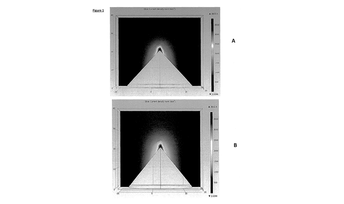
Figure 1 shows a computer model of current density when passed through a
surface structure with a
triangular cross-section. The darker colour at the apex of the structure
indicates a higher distribution of
current density. The same figures are shown in colour (A) and black and white
(B).
Figure 2 shows a computer model of current density when passed through a
surface structure with a
semi-circular cross-section. The darker colour at the apex of the structure
indicates a higher distribution
of current density. The same figures are shown in colour (A) and black and
white (B).
Figure 3 shows a comparison between the charge density (voltage or current)
ranges observed for a flat
sensing surface versus an array of sensing surfaces on tips.
Figure 4 shows a cross-sectional view of an electrode array according to the
invention with a triangular
cross-section.
Figure 5 shows an embodiment of the invention in which the active species
comprises a catalyst,
wherein the catalyst is activated via electrochemical modification following
contact with the functional
surface to yield an activated catalyst.
Figure 6 shows a Cu(I) catalysed azide alkyne cycloaddition reaction with an
ethynyl fluorophore (A)
Figure 7A shows a negative fluorescence image of an array with no potential
applied and figure 7B
shows a negative fluorescence image of an array with a reductive potential
applied to activate the
copper catalyst.
Figure 8 shows the desorption profile of a SAM attached to an electrode layer
for (A) pyramidal surface
structures and (B) a flat surface.
Figure 9 and 10 show SEM images illustrating the Pt deposition at the apex of
a group of surface
structures.
Figure 11 shows an AFM analysis of a typical 'flat' surface showing particle
sizes of "< 100 nm in a closely
packed formation.
Figure 12 shows a graph associated with Figure 11 showing the topography, and
the relative height of
the particles.
Figure 13 shows an SEM image of an array of approximately 100nm tips in
polymer.
Figures 14 - 16 show the comparison in the activity for typical flat vs nano-
structured electrodes for both
Hydrogen production and Oxygen reduction by an Au electrode and Pt electrode
using a 3D surface to
control the distance between and the location of the particles.
Figure 17 shows an SEM of the surface of the pure nickel structure from Table
1.
Figure 18 shows the effect of changing the pulse frequency of the
electrochemical "Click" reaction on
the ferrocene surface coverage, (triangles high, circle medium and squares low
frequencies).
Figure 19 shows the pictorial representation of the control on the extent of
surface functionalization at
the apex at different frequencies
CA 03042379 2019-04-30
,
WO 2018/106128 PCT/NZ2017/050160
Figure 20 shows cyclic voltammetry of immobilised ferrocene on Pyramidal
electrode
Figure 21 shows cyclic voltammetry of immobilised ferrocene on flat electrode
Figure 22 shows the
ascorbic acid oxidation in the absence of ferrocene on SAM coated Pyramid
(solid line) and flat (dashed
line).
5 Figure 23 shows the ascorbic acid (1m M) oxidation by ferrocene
immobilised on pyramid (solid line) and
flat (dashed line)
Figure 24 shows the ascorbic acid (100 mM) oxidation by ferrocene immobilised
on pyramid (solid line)
and flat (dashed line)
10 .. Detailed Description of the invention
Definitions
"Attach" or "bind" means covalent bonding, electrostatic bonding or some other
bonding mode where
the species is bound in some way to the support. Attachment may be direct or
via another species.
"Tapered" means moving from a wider surface structure to a narrower surface
structure.
15 "Smooth" means substantially no changes in the rate of change of angles
of a surface.
"Deposited" means formed on a surface and may refer to any form of formation,
layering or production.
In one embodiment, the deposition is achieved by sputtering, e-beam or thermal
evaporation.
Preferably the deposited layer has some degree of adherence to the layer on
which it is deposited. This
adherence may be covalent, electrostatic or include Van der Waals forces.
20 "Substantially constant thickness" in relation to the electrode layer
means that the electrode layer does
not vary significantly over the extent of its coverage of the support
substrate or binding layer.
Unintentional variations in the thickness of the layer that have substantially
no effect on function of the
sensor are intended to be incorporated by the term substantially constant
thickness.
"Comprise", "comprising", and the like, are, unless the context clearly
requires otherwise, to be
25 construed in an inclusive sense as opposed to an exclusive or exhaustive
sense, that is to say, in the
sense of "including, but not limited to".
The terms "Surface structure" and "functional surface" as referred to herein
are intended to refer to
singular or plural structure/surfaces.
"Width" of a surface structure is measured by the greatest distance across a
cross-sectional area of the
surface structure where the cross-section is taken along a plane substantially
parallel to an upper
surface of the support substrate. Where width is referred to, the point on the
surface structure at
which the parallel plane occurs is also described (e.g. at the joint between
the support substrate and the
surface structure).
"Catalyst" refers to the species that increases the rate of a chemical
reaction.
CA 03042379 2019-04-30
WO 2018/106128 PCT/NZ2017/050160
26
"Electrochemically modified" in relation to an active species means that the
active species undergoes
reduction or oxidation i.e. gain or loss of electrons.
"Solute reactant" means a reactant found in the solution which takes part in a
reaction catalysed by a
catalyst active species. The solute reactant will preferably be in another
conductive solution (i.e.
different to the conductive solution comprising the active species) or may be
in the same solution and
will once reacted with the active species serve to bind/react with a target
molecule to be detected by
the sensor (refer "attached product" below).
"Binding layer" comprises a layer of molecules attached to a surface of the
electrode array. The binding
layer may be formed from a cross-linked polymer, a photo-resist or a self-
assembled mono-layer (SAM).
Preferably the cross-linked polymer is an epoxy-based negative photoresist
such as SU-8. The binding
layer may be deposited onto the surface of the electrode array by means known
to those of skill in the
art, for example by spin-coating, spray-coating, dip-coating, wiping or
painting. In alternative
embodiments, the binding layer is attached to a surface of the electrode array
by electrochemical
modification of a precursor to a binding layer (i.e. an active species),
preferably according to the
methods described herein.
"Attached product" is the product of a reaction between a solute reactant and
a binding layer, wherein
a catalyst catalyses said reaction. In other words, it is the bond / linger
that forms upon binding
occurring.
"Detection moiety" comprises a component capable of attachment (directly or
via another functional
group) to a binding layer and which is capable of detection using detection
techniques known to those
of skill in the art. For example such techniques selected from the group
consisting of protein detection,
colorimetric detection, electrochemical, chemiluminescence detection,
fluorescence detection,
bioluminescence, chemifluorescence or radiographic detection. Where detection
moieties are
employed, they may be detected by standard methods known to those of skill in
the art, for example
fluorescence, optical or colourimetric measurements may be carried out.
"Focussed" in relation to an electrical current or voltage means that the
charge density (voltage or
current) is stronger in a focused position on a surface compared to another
position on a surface.
Charge density (voltage or current) on a surface can be measured according to
methods known to those
of skill in the art. However, in one embodiment, the charge density (voltage
or current) is measured by
modelling, and then directed attachment of a fluorophore, or platinum
deposition on the surface.
"Counter electrode" the counter electrode may be any conductive entity that
facilitates a current flow
from the electrode layer through the solution. In one embodiment, the counter
electrode comprises a
wire or other form of electrode structure held within the solution. Preferably
the counter electrode is
formed from a material selected from the group consisting of a metal, Pt,
Gold, nickel, copper, iron,
CA 03042379 2019-04-30
. õ
W02018/106128 PCT/NZ2017/050160
27
carbon, graphite, graphene, carbon fibre, carbon nano-tubes, Bucky Balls,
conducting polymer PPy, PA,
Polycetylene, stainless steel. The counter electrode may be made of a solid
layer or the conducting
layer deposited onto a suitable support e.g. polymer glass, metal. The counter
electrode may also be a a
bare metal (Au, Pt, Stainless steel, copper) or an Au or Pt plated substrate
(metal, polymer or glass), and
may have 3D surface features which are configured in such a way as to promote
the location of the
charge density (voltage or current) on the 3D working electrode. For example,
it may be a series of tips
that reflects the tips of the working electrode.
"Activating" or "activate" means to convert an active species from an inactive
form to a reactive form.
Thus, "electrochemical activation" means to convert the active species into a
reactive form by oxidising
or reducing it by applying a current at an electrode.
"Activating potential" means the voltage (oxidative or reductive in the
typical range between +2V and -
2V) required to initiate a coupling/attachment/modification reaction.
Typically a reductive activating
potential for click is from -500mV to -100 mV.
"Inactivating potential" means the voltage required to stop a
coupling/attachment/modification
reaction
"Active species" means an entity present in the solution which has the
potential to undergo
electrochemical modification. In one embodiment, the active species is a
catalyst or a catalyst
precursor. In another embodiment, the active species is a component of a
binding layer. In another
embodiment, the active species is a charged particle capable of attachment to
a functional surface. In
another embodiment, the active species is a binding agent capable of detecting
a target analyte in the
solution.
"Oxidation" means a chemical reaction involving the loss of electrons.
Therefore, "oxidative" means
facilitating the loss of electrons in a chemical reaction.
"Reduction" means a chemical reaction involving the gaining of electrons.
Therefore, "reductive" means
facilitating the gaining of electrons in a chemical reaction.
"Pulsed" or "pulsing" means to modulate a voltage or current from an
activating potential to an
inactivating potential. Pulsing may be regular or intermittent.
"Self-assembled monolayer (SAM)" means molecular assemblies comprising head
groups linked to a tail
group which terminates with a functional group.
"Selective removal" in reference to removal of an entity from a functional
surface means that the
removal is enhanced when compared to another surface on the array at which
current is not focussed.
For example the removal of a SAM will occur at a faster rate, or a greater
concentration of the entity will
be removed when compared to those other surfaces. This wording does not imply
that removal is
complete or that removal does not occur to a lesser degree on other surfaces.
CA 03042379 2019-04-30
WO 2018/106128
PCT/NZ2017/050160
28
"Selective deposition" in reference to deposition of an entity on a functional
surface means that
deposition is enhanced when compared to another surface on the array at which
current is not focused.
For example the deposition of a SAM will occur at a faster rate, or a greater
concentration or density of
the entity will be deposited compared to those other surfaces. This wording
does not preclude the
possibility that deposition occurs to a lesser degree on other surfaces.
"Functionality" means any feature capable of attachment to a surface which has
a function. For
example binding layers, binding agents, active species, detection moieties,
charged particles and
attached products are all functionalities.
"Salvation" (or solvated) is an interaction of a solute with the solvent,
which leads to stabilization of the
solute species in the solution.
Description
Applications involving modification and functionalisation of surfaces suffer
from a lack of options to
position functional groups, binding layers or ionic substances. The lack of
options to date has meant
that the sensitivity and selectivity of sensors and catalytic arrays has been
limited. The inventors have
found that when current or voltage is passed through an electrode array
exposed to an electrolyte
solution, charge density (voltage or current) can be focussed towards the top
of surface structures.
They have advanced this concept to develop an electrode array with a
functional surface which can be
selectively functionalised by deposition or removal of binding layers, binding
agents, active species or
other functionality at or about an apex of each surface structure.
Figures 1 and 2 illustrate a computer model (COMSOL) of current passing from a
surface structure on a
flat base into a solution. This indicates that the charge density (voltage or
current is highest at or about
the apex of the structure. The modelling also suggests that the aspect ratio
(sharpness) and the shape
of the structure affect the distribution of charge density (voltage or
current). The inventors have found
that active species in a solution can be electrochemically modified via
contact with the functional
surface at which charge density (voltage or current) is focussed to enable
precise location and
deposition of functional groups, binding layers, ionic substances or other
functionalities on a surface.
The inventors have also shown that the same effect of focussing charge density
(voltage or current) at
the surface can be used to selectively remove functional groups, binding
layers, ionic substances or
other functionalities from a surface. While the sharper the point at the apex
of the surface feature is
the more precise deposition is (as the charge density is more focussed at the
tip, more rounded options
may also be used should that be desired.)
CA 03042379 2019-04-30
WO 2018/106128 PCT/NZ2017/050160
29
This invention is directed to the application of three dimensionality for
catalysis and sensing.
Features/results include:
= Kinetic enhancement, i.e. a dramatic increase in the rate of catalysis
and the rate of binding of a
capture agent. This kinetic effect is obvious to anyone in the field when
observing the results
herein (see Example 6 and 8 and the Tables below).
= Thermodynamic enhancement, i.e. a dramatic decrease in the energy
required to drive a redox
catalytic reaction for both metallic and organometallic electrocatalysts. The
enhancements
achieved are in the order shown in Examples 6 and 8, and the Tables below.
Metallic catalyst
02 reduction H2 production
Voltage shift Power gained at peak Voltage shift
Power gained
rel. to flat rel. to flat rel. to flat rel. to flat 15
Pt (Nano) 200 mV 1500%
Au (Nano) 60 mV 850%
Ni (Nano) 100 mV 770% 20
Pt (Pyramid) 65 mV 250%
25 Organometallic catalyst (comparison of pyramid vs flat only)
Ascorbic acid oxidation
Voltage shift Power gained rel.
rel. to flat to flat
Ferrocene (pyramid) 59 mV 152 %
The invention is based on one or more of the following non-limiting concepts:
1. Selective functionalization using a redox process at a predefined location
on a surface using either
30 voltage or current density distribution localised at the apex of a
structure (tip or a line).
= The sharper the tip, the more focused the functionalisation.
= The higher the frequency, the more focused the functionalisation. (for
example see example 7)
Examples include:
= Selective attachment using a redox mediated reaction
35 = Selective metal deposition
CA 03042379 2019-04-30
WO 2018/106128 PCT/NZ2017/050160
= Selective desorption of a self-assembled monolayer (could be applied to
non-specific binding of
matrix proteins)
2. Enhancement of an electro-catalytic process, by reducing the thermodynamic
energy cost and
increasing the kinetic turn-over.
5
The invention has particular application in the fields of biosensors,
electrochemical sensing, optical
sensing, electrocatalysis or selective deposition of material. Further
applications could also include
displays, signs, active surfaces and other applications requiring attachment
of functionalities onto a
surface.
Figure 3 shows the separate (A and B) and overlapped (C) cyclic voltammograms
for both flat (A) and tip
(B) electrodes for Ferrocyanide (0.1mol) in phosphate buffer relative to a
Ag/AgCI reference electrode.
The cyclic voltammetry traces shown take into account the relative area of the
electrodes and
demonstrates the dramatic increase in the signal, and hence signal to noise
obtained for an array of
71.i.m tips verses a flat electrode. The inset figure A shows a response range
of approximately 21.tAcm 2.
In contrast, the inset figure B shows a response range nearly 8000 times
larger at 16000 pAcm2for the
same surface area. This effect occurs in microelectrodes due to spherical
diffusion towards the tips,
rather than planar diffusion which is seen for a flat electrode.
Selective functionalisation of the upper portion of the surface structures
enables electrode arrays to be
produced with diversity of attached functionalities on the same electrode
surface. For example, an
electrode surface with positionally distinct functionalities may be prepared
by electrochemically
depositing a functionality A at or about the apex of a surface structure and a
different functionality B
bound to the remainder of the electrode surface (i.e. on the surface between
the functional surfaces of
the surface structures).
The present invention has a number of applications including:
= digital sensing (high resolution pixilation for optical sensing);
= detection of generated analytes as a consequence of the high surface area
of the electrode
array;
= mass producing high aspect ratio conducting polymer forest/grass for
sensing application; and
= catalysis.
= Photovoltaics
CA 03042379 2019-04-30
WO 2018/106128 PCT/NZ2017/050160
31
The invention therefore provides a method of focussing charge density (voltage
or current) at a
functional surface on an electrode array, the method comprising the steps of:
a. providing an electrode array comprising:
i. a support substrate;
ii. at least one surface structure protruding from an upper surface of the
support
substrate wherein the surface structure includes an electrode layer;
iii. a functional surface on the electrode layer, wherein the functional
surface is on
an upper portion of the at least one surface structure and wherein the
functional surface is adapted to contact an active species in a solution;
b. exposing the surface structure to a conductive solution containing an
active species in
which a counter electrode is positioned; and
c. establishing a current or voltage between the functional surface on
the electrode layer
and the counter electrode such that the charge density is focussed at the
functional
surface on the electrode layer.
Preferably the functional surface is at or about an apex of the surface
structure of the array.
In a more preferred form, the functional surface is at or about an apex of the
surface structure and the
apex is tapered to an apex and/or has a substantially triangular cross-section
along a plane parallel to a
top surface of the support substrate.
It is also preferred that the functional surface is at or about an apex of the
surface structure and
wherein the width of the apex of each surface structure is between about mm to
about 5000 micron.
Further options of use are described herein but would be apparent to a skilled
reader.
It is also preferred that the functional surface is at or about an apex of the
surface structure and
wherein the width of the surface structure where it joins the support
substrate is between about 20nm
to about 5000p.m (further options of use are described herein but would be
apparent to a skilled reader)
and wherein the width at the apex of the surface structure is less than the
width of the surface structure
where it joins the support substrate.
It is also preferred that the functional surface is at or about an apex of the
surface structure and
wherein the apexes of the surface structures are separated from each other by
about 50 nm to about
1000p.m apex to apex (further options of use are described herein but would be
apparent to a skilled
reader).
While the surface structures may be of any form as is described herein, it is
preferred that they are
pyramidal, conical, ridges, or combinations thereof, and it is also preferred
that the counter electrode
structure is also flat, pyramidal, conical, or ridged.
In a preferred form, the shape of the counter electrode reflects that of the
surface structures and, in a
more preferred form, the counter electrode is parallel to the surface
structures.
The functional surface will preferably comprise a catalyst capable of
electrochemical activation.
CA 03042379 2019-04-30
4
WO 2018/106128 PCT/NZ2017/050160
32
In a preferred form the functional surface is formed of a catalytic material
(e.g. Pt, Au, Ni) which is
activated via electrochemical modification via the current or voltage between
the electrode layer and
the counter electrode.
When the functional surface comprises a catalyst (including when it is formed
of a catalytic material), it
is preferred that the catalyst is activated via application of a current or
voltage to yield an activated
catalyst and the catalytic turnover rates (thermodynamic and kinetic) compared
to the same material on
a flat surface are improved.
The catalyst will preferably be selected from metallic and organometallic
materials, and the metallic
materials are preferably selected from one or more of Pt, Au and Ni, and the
organometallic material is
selected from one or more of Ferrocene, and Porphyrin, or Phenanthroline,
Porphyrin, Imidazole, tris
pyridyl amine, and triazole, with a transition metal. Preferably the
transition metal is selected from any
one or more of Ru, Fe, Mn, Mg, Cu, Ir, Co, Pt, Pd, Au, Ag, Mg. (Ferrocene
already including a transition
metal and Porphyrin may optionally include a transition metal).
It is also preferred that the active species is electrochemically modified
following contact with the
functional surface. Preferably the active species is electrochemically
modified following contact with the
functional surface and the thermodynamic efficiency and kinetic efficiency of
the electrochemical
modification is improved compared to a corresponding flat electrode.
The electrode array of the invention also preferably comprises a binding layer
which is either present on
the functional surface at a significantly increased density than at a non-
functional surface on the
electrode array; or present on a non-functional surface of the electrode array
at a significantly increased
density than at a position on the functional surface on the surface structure.
The binding layer will preferably comprise a self-assembled monolayer (SAM) as
is described in more
depth herein.
In another preferred option, the array includes a catalyst at the apex of the
surface structure and a co-
catalyst in the valleys between the surface structures, wherein the catalysts
are selected as described
above, and the co-catalysts are selected from any one or more oxides of a
metal (e.g. ruthenium, nickel,
aluminum, calcium, cerium, gallium, hafnium, iron, lanthanum, magnesium,
strontium, titanium,
zirconium,or zinc).
The method also achieves an increase in the rate of catalysis compared with a
flat electrode (Kinetic
efficiency ¨ i.e. the speed at which catalysis occurs, and relating primarily
to the speed at which the
CA 03042379 2019-04-30
'
WO 2018/106128 PCT/NZ2017/050160
33
reactants and the products diffuse to and away from the catalytic surface.).
The method also achieves a
decrease in the energy required to drive a redox catalytic reaction for both
metallic and organometallic
electrocatalysts (Thermodynamic efficiency - i.e. the energy required to drive
the electrocatalytic
reaction)
Preferably the method achieves increases in both Kinetic and Thermodynamic
efficiency compared to an
electrode with a flat surface.
In another aspect, the invention provides a method of focussing charge density
(voltage or current) at a
functional surface on an electrode array, the method comprising the steps of:
a) providing an electrode array comprising
i) a support substrate;
ii) at least one surface structure protruding from an upper surface of the
support substrate
wherein the surface structure includes an electrode layer;
iii) a functional surface on the electrode layer, wherein the functional
surface is on an upper
portion of the at least one surface structure and wherein the functional
surface is adapted
to contact an active species in a solution;
b) exposing the surface structure to a solution comprising both an active
species and a counter
electrode that is positioned therein; and
c) establishing a current or voltage between the electrode layer and the
counter electrode such
that the charge density is focussed at the functional surface and the active
species is
electrochemically modified following contact with the functional surface.
Preferably the functional surface is at or about an apex of the surface
structure. It will be appreciated
by those of skill in the art that surface structures with an apex are likely
to be substantially flat when
viewed at very high magnification. Accordingly, the shapes and measurements
provided herein are
intended to refer to the overall shape of the surfaces structure rather than
being precise geometric
descriptions.
In this aspect, charge density (voltage or current) is focussed on the upper
portion of the surface
structure ¨ referred to as the functional surface. The inventors have shown
that this effect, when put
into effect with appropriately shaped surface structures, can be used to
selectively functionalise or de-
functionalise the upper portion of the surface structures where they contact a
solution.
CA 03042379 2019-04-30
a ,
WO 2018/106128 PCT/NZ2017/050160
34
In a first embodiment, the active species comprises a catalyst, wherein the
catalyst is activated via
electrochemical modification following contact with the functional surface to
yield an activated catalyst.
Figure 4 shows an embodiment of the invention in which the electrode array 400
comprises a support
substrate 410, surface structures 415 and an electrode layer 420. The
electrode layer is overlaid with a
binding layer 430 onto which are attached terminal functional groups 440. In
another embodiment, the
functional surface is formed of a catalytic material (e.g. Pt, Au, Ni) which
is activated via electrochemical
modification via the current or voltage between the electrode layer and the
counter electrode.
The electrode array of figure 4 is shown in figure SA submerged in an
electrolyte solution 500 containing
an active species (not shown), several solute reactant particles 510 and a
counter electrode 520. When
a current is established between the electrode layer 420 and the counter
electrode (see figure 56), the
active species ¨ a catalyst in solution ¨ is activated and catalyses the
reaction of the solute reactant with
the functional groups R on the binding layer in an active region at or about
the apex of the surface
structures. The solute reactant may be in either the same or a different
conductive solution to the
active species. The active region being created by the interaction of the
functional surface on the
electrode layer and the positioning of the counter electrode. This is possible
due to the focussing of the
charge density at the top of the functional surface as has been previously
been discussed (see Figures 1
and 2). Figure SC shows the selectively functionalised surface structures with
the functionality localised
at or about the apex of the surface structures.
As will be apparent to the skilled reader, where the description of the
invention refers to a solution
comprising both an active species and a counter electrode, this refers to the
solution having the counter
electrode position therein.
The catalyst may be any suitable catalyst which is activated by oxidation or
reduction at a charged
surface. In particular embodiments the catalyst comprises a charged metal
species such as transition
metals like copper, Cr, Ag*, Pt2*, Pd2*, Fe2*, Ir2+, Ni24, Rd, Co, Mn, Ru,
Such catalysts will typically occur in two or more oxidation states and will
be active in catalysing a
reaction of a solute reactant with a binding layer in one state and inactive
in at least one other oxidation
state. The catalyst is preferentially activated at the area of charge focusing
(voltage or current) (on the
upper portion of the surface structures) as compared to other surfaces on the
array, for example on the
support substrate, the electrode layer on a lower portion of the surface
structures, or on the binding
layer on the lower portion or between surface structures. As such,
electrochemical activation of the
CA 03042379 2019-04-30
W02018/106128 PCT/NZ2017/050160
catalyst occurs at a substantially greater rate at the functional surface than
activation would occur at
another surface position on the electrode layer.
The effect described above enables the method of the first aspect to be
extended to further comprise
5 the step of electrochemically activating the active species in the
solution to yield an activated catalyst.
The further step of attaching a solute reactant to a binding layer on the
functional surface can be
achieved once the catalyst is activated.
In one embodiment, the current established between the electrode surface and
the counter electrode
10 activates (reduces) Cu(II) which contacts the functional surface to
Cu(I). The Cu(I) catalyses the azide
alkyne cycloaddition reaction shown in figure 6. Figure 6 also shows an
ethynyl fluorophore detection
moiety (A) which is attached to the surface following cycloaddition. Example 2
provides experimental
details of the Cu(I) catalysed azide alkyne cycloaddition reaction. Figure 7A
shows a negative
fluorescence image of an array with no potential applied and figure 78 shows a
negative fluorescence
15 image of an array with a reductive potential applied to activate the
copper. The dark patches are the
fluorophores fluorescing. Negative images are used to more clearly represent
the areas of fluorescence
and enable clear representation in black and white. The attached fluorophores
are visible on the upper
portions of the surface structures in figure 78 but substantially absent from
figure 7A (the control).
Preferably, the activated catalyst catalyses a reaction of a solute reactant
with a binding layer to yield an
20 attached product on the functional surface. The Cu active species can be
any other suitable catalyst that
is activatable by redox type reactions at a charged surface, such as the metal
and organometallic active
species discussed herein.
Preferably the active species comprises copper (II) and the electrochemically
activated catalyst
25 comprises copper (I).
Preferably the reaction between the solute reactant and the binding layer is a
copper (I) catalysed azide
alkyne cycloaddition reaction.
Preferably the solution comprises a buffer solution with alkali metal chloride
ions and copper' ions.
Preferably the solute reactant comprises a compound with a reactant group that
is able to couple to the
surface and a functionality (e.g. for sensing, catalysis, optics, further
attachment).
CA 03042379 2019-04-30
WO 2018/106128 PCT/NZ2017/050160
36
Preferably, the solute reactant is selected from the group consisting of but
not limited to alkynes,
alkenes, carboxylic acids, esters, ketones, aldehydes, alcohols and amines.
Preferably the alkyne
comprises acetylene.
Preferably the solute reactant comprises a detection moiety adapted to attach
to the functional surface
following reaction of the solute reactant with the binding layer.
Preferably the detection moiety is capable of detection using protein
detection, electrochemical
detection, amperiometric, current, voltage, capacitance, colorimetric
detection, chemiluminescence
detection, fluorescence detection, bioluminescence, chemifluorescence or
radiographic detection.
Preferably, the solute reactant with detection moiety comprises an ethynyl
functionalised fluorophore,
Preferably the binding layer to which a solute reactant binds comprises a self-
assembled monolayer
(SAM).
The SAM may be functionalised with a functional group to provide it with a
desired functionality.
Preferably, the active species comprises a solute reactant capable of
attachment to the binding layer.
Preferably the binding layer is present on at least one of:
= the functional surface;
= the surface structures;
= the passivating layer; or
= the support substrate.
Preferably the method of the first embodiment of the invention further
comprises depositing a SAM on
at least one of:
= the functional surface;
= the surface structures;
= the passivating layer; or
= the support substrate.
Preferably the step of depositing the SAM is carried out prior to
electrochemically activating the active
species following contact with the functional surface to yield an activated
catalyst.
Preferably the step of depositing the SAM is carried out prior to attaching a
solute reactant to a binding
layer on the functional surface.
CA 03042379 2019-04-30
WO 2018/106128
PCT/NZ2017/050160
37
In a particular embodiment, the binding layer is selected from the group
consisting of azides, carboxylic
acid, amine, alcohol, ester, ketone, cyano and aldehyde.
Preferably the binding layer on the functional surface is substantially stable
for the duration of the
current flow between the electrode layer and the counter electrode. To
maintain a stable binding layer
the SAM preferably comprises a carbon chain of C6 to C16 (C6, 7, 8, 9, 10, 11,
12, 13, 14, 15, or 16). For
better stability, the SAM preferably comprises a carbon chain of C11 to C16
(C11, 12, 13, 14, 15, or 16).
The carbon chains can be an alkane, alkene, alkyne and aromatic structure.
Mixtures of carbon chains as
referred to above (of C6 to C16, preferably C11 to C16), of any structure may
also be used.
Preferably the attached product is selected from the group consisting of:
a. a functional group, for example one selected from the group consisting
of carboxylic acid,
amine, alcohol, aldehyde, biotin, avidin, azide and ethynyl;
b. a binding agent adapted to bind to a target analyte in solution, for
example one selected from
the group consisting of antigens, antibodies, antibody fragments, single-chain
variable
fragments, biotinylated proteins, peptides, nucleic acids, avidin,
streptavidin, NeutrAvidin,
recombinantly expressed proteins containing polyhistidine or glutathione S-
transferase,
atetylenic quinone, azides, tetrazine, large or small amine-containing
molecules, sulfhydryl-
containing molecules or proteins expressing glutathione S-transferase (GST),
metals and metal
salts (such as lead, lead phosphate, chromium, platinum, palladium, iridium,
copper), ssDNA,
ssRNA, miRNA, mRNA, aptamers, and small molecules with and without a spacer
molecule;
c. a catalytic species which catalyses a reaction in solution, for example
a catalyst selected from
the group consisting of copper, a transition metal, an organometallic complex,
an
organometallic complex including transition metal, or an organic material that
is able to be
oxidised or reduced; and
d. a detection moiety, for example one selected from the group consisting of a
fluorophore, an
ethynyl functionalised fluorophore, a protein, an antibody, a nucleic acid,
DNA, RNA, a small
molecule, or a functional group, for example one selected from the group
consisting of
carboxylic acid, amine, alcohol, ester, ketone and aldehyde.
Preferably the attached product is selected from the group consisting of
triazoles, amides, quinones and
esters or mixtures thereof.
Preferably the attached product is selected from the group consisting of
triazoles, amides, quinones and
esters, or Pt, Ir, Au, Ag, Fe, and mixtures thereof.
CA 03042379 2019-04-30
WO 2018/106128
PCT/NZ2017/050160
38
It will be understood by those of skill in the art that removal of a binding
layer such as a SAM is very
difficult using manual means or other means described in the prior art. Even
more challenging is the
selective removal of a SAM from a specific location on a surface, to produce a
regular patterned array of
exposed surface for subsequent functionalisation or reaction. If high currents
(for example greater than
about 2V) are applied across the surface, electrolysis of the solution can
occur yielding oxygen or
hydrogen at the electrode layer. This is undesirable and can affect
measurements and reactions which
occur at the surface. Another problem is the undesirable stripping of the
electrode layer from the
surface. In this case, the electrode layer (often gold or another precious
metal) can be lost to the
solution. Preferably therefore the current applied is less than 2V and more
preferably less than 1V,
between 0 and 1V (0.1, 0.2, 0.3, 0.4, 0.5, 0.6, 0.7, 0.8, 0.9)
The inventors have shown that the focussing of charge density (voltage or
current) at the functional
surface on an upper portion of the surface structure can be used to
selectively attach or remove binding
layers to the functional surface, preferably without the electrolysis of water
nor the removal of the
electrode layer.
Accordingly, in one embodiment, the electrode array of the invention comprises
a binding layer
(preferably a SAM) covering the functional surface and at least part of other
surfaces of the array,
wherein the step of establishing a current between the electrode layer and the
counter electrode results
in selective removal of the binding layer from the functional surface compared
to other positions on the
electrode array. The inventors demonstrate in example 3 the selective removal
(desorption) of a SAM
from the upper portion of surface structures.
Preferably the method of the invention further comprises the step of selective
removal of at least part
of the binding layer from the functional surface as compared to other
positions on the electrode array.
Preferably the method of the invention further comprises the step of selective
deposition of a further
binding layer on the functional surface which has undergone selective removal
of the first binding layer.
Example 5 shows an example of the deposition of a first binding layer (SAM) on
an electrode array, then
selective removal of the binding layer from the functional surface at or about
the apex of the surface
structures of the array followed by deposition of a different binding layer
(SAM) at or about the apex.
The removal of the binding layer from the upper portion of the surface
structure enables a binding layer
comprising functionalities to be selectively attached at or about the apex of
the surface structure. This
CA 03042379 2019-04-30
WO 2018/106128 PCT/NZ2017/050160
39
can be used for attachment of binding agents and/or detection moieties, for
example for use as
biosensors for testing of solutions for target analytes.
Removal of the binding layer at the functional surface is made possible by
electrochemical modification
of an active species in the solution where the active species is solvated
within a charge carrying or ionic
species, for example selected from the group consisting of a buffer, a salt
species, and NaCI. The active
species preferably acts as an electron donor and provides the binding layer,
for example the sulphur on
the SAM, with an electron thus liberating the SAM. The binding layer may
comprise a number of
different molecules or atoms which are susceptible to reduction or oxidation
by the charged active
species, for example S, 0 or N. The effect of the electrochemical modification
of the active species is the
oxidation or reduction of the functionality on the binding layer that binds to
the functional surface (e.g.
the S atom of the SAM).
Preferably the electrochemical modification of the active species comprises
either a partial or full
oxidation or reduction.
In one particular embodiment, the electrode array comprises a binding layer on
a lower portion of the
surface structure but absent from an upper portion of the surface structure,
and the method further
comprises the step of selective deposition of a further binding layer on the
functional surface.
In this embodiment, an electrode array previously prepared with the binding
layer removed from the
upper portion is selectively functionalised at the functional surface ¨ i.e.
on the upper portion of the
surface structure.
.. Preferably the electrode array defined in the first aspect further
comprises a self-assembled monolayer
(SAM).
Preferably the SAM is present on an upper surface of the electrode layer.
Preferably the SAM is present on an upper surface of the support substrate.
Preferably the SAM is present around the surface structures such that the
surface structure or a portion
thereof protrudes with an exposed functional surface thereon.
CA 03042379 2019-04-30
=
WO 2018/106128 PCT/NZ2017/050160
Preferably the SAM comprises long-chain molecules comprising a carbon chain of
C6 to C24 (C6 7 8 9 10
11 12 13 14 15 16 17 18 19 20 21 22 23 or 24) in alkane, alkene, alkyne, or
aromatic structures; or
mixtures thereof. In this embodiment, the stability of the SAM is increased
relative to a shorter carbon
chain. In turn this requires a stronger current to destabilise and remove the
SAM.
5
Preferably the SAM comprises short-chain molecules comprising a carbon chain
of C5 to Cl (Cl 2 3 4 5).
In this embodiment, the SAM is less stable and therefore requires a weaker
current. It is therefore
more susceptible to removal and this may be preferable for applications that
require fast removal of the
SAM.
Preferably the SAM is a mixed SAM comprising long and short chain molecules.
Preferably the mixed SAM comprises long-chain molecules comprising a carbon
chain of C6 to C24 and
short-chain molecules of C5 to Cl (all of which are referred to above).
Preferably the long-chain SAM comprises molecules selected from the group
consisting of azides,
amines, carboxylates or carboxylic acids.
Preferably the short-chain SAM comprises molecules selected from the group
consisting of alkanes,
azides, amines, hydroxyls, carboxylates or carboxylic acids.
In one particular embodiment, the SAM comprises a mixture of long chain
molecules comprising
carboxylic acid molecules of C6 to C24 (as defined above) and short chain
molecules (as defined above)
comprising hydroxyl molecules. In the above embodiments, the SAM long chain
molecules are
preferably selected from C6, C8, C10, C12, C14, C16, C18 or C20 molecules.
Preferably the SAM is present on the electrode array but is absent at the
upper portion of the surface
structure as defined above.
Preferably the SAM comprises long-chain molecules comprising a carbon chain of
C6 or more (to C24 as
defined above) or short-chain molecules C5 or less (to Cl as defined above)
and wherein the upper
portion of the surface structure(s) is either a. free of SAM, or b. comprises
a SAM adapted to be
removed by establishing a current between the electrode layer and the counter
electrode.
CA 03042379 2019-04-30
WO 2018/106128 PCT/NZ2017/050160
41
Preferably the SAM comprises an long chain molecule with a carbon chain of
between C6 to C24, and
wherein the upper portion of the surface structure(s) is either a. free of
SAM, or b. comprises a SAM
adapted to be removed by establishing a current between the electrode layer
and the counter
electrode.
In one particular embodiment exemplified in example 5, the electrode array
comprises a SAM binding
layer on an upper and lower portion of the surface structure and contact of
the active species with the
functional surface results in selective removal of the SAM binding layer from
the upper portion of the
surface structure where charge density (voltage or current) is focussed. In
this embodiment, the
method further comprises the step of selective deposition of a further binding
layer on the now exposed
portion of the electrode layer at the functional surface.
Preferably the SAM is selected from the group consisting of alkane thiols with
a terminal methyl, azide,
thiol, aldehyde, cyano, diazonium, amines, alcohols, silanes, phosphonic acids
and carboxylic acids.
In particular embodiments, the SAM comprises:
R-(CH2)9-SH, R-(CH2)0-NH2, or
11-(CH2)n-Si(01113
wherein R = alkyl, azide , quinone or tetrazine; and
R' = Me, CI, Et; and
wherein n=1 to 50
The method of the invention may comprise selective deposition of a further
binding layer on the
functional surface as compared to other positions on the array. This step may
be carried out on an array
which has already undergone selective removal of a binding layer (e.g. a SAM)
from the functional
surface.
Preferably the further binding layer comprises a functional group selected
from the group consisting of
SAM-COOH, SAM-C-NH2, SAM-N3, wherein SAM comprises a self-assembled monolayer.
Preferably the step of deposition of a further binding layer comprises
coupling of an active species to
the binding layer on the functional surface. Preferably the coupling comprises
a 1-Ethy1-3-(3-
dimethylaminopropy1)-carbodiimide/N-hydroxysuccinimide (EDC/NHS) coupling
reaction.
Preferably the binding layer further comprises a binding agent. The binding
agent is preferably capable
of binding to a target analyte within a solution. For example the binding
agent is selected from the
group consisting of antigens, antibodies, antibody fragments, single-chain
variable fragments,
CA 03042379 2019-04-30
WO 2018/106128 PCT/NZ2017/050160
42
biotinylated proteins, peptides, nucleic acids, avidin, streptavidin,
NeutrAvidin, recombinantly expressed
proteins containing polyhistidine or glutathione S-transferase, atetylenic
quinone, azides, tetrazine,
large or small amine-containing molecules, sulfhydryl-containing molecules or
proteins expressing
glutathione S-transferase (GST), metals and metal salts (such as lead, lead
phosphate, chromium,
platinum, palladium, iridium, copper), ssDNA, ssRNA, miRNA, mRNA, aptamers,
and small molecules
with and without a spacer molecule.
Preferably, the active species comprises an entity with potential for
electrochemical reduction or
oxidation. Preferably the active species comprises a binding agent as
described above or a functional
group capable of attachment to the binding layer. Preferably the functional
group is selected from the
group consisting of avidin, cyano, aldehyde, ester, ketone, COOH, NH2, azide,
ethynyl, bioactive biotin,
quinone and tetrazine or combinations thereof.
The inventors have also found that the focussing of charge density (current or
voltage) on a functional
surface can be used to attach particles to the functional surface following
the electrochemical
modification.
Accordingly, in a further embodiment of the invention, the active species
comprises a species wherein
the species is attached to the functional surface following the
electrochemical modification.
Preferably the active species is a charged particle preferably selected from a
metal ion(s). Preferably the
metal ion comprises an ionic form of platinum, gold, palladium, Iron, Iridium,
silver, copper, an alloy or a
transition metal.
Preferably the ionic form is an oxidised form of the metal ion.
Preferably the ionic form is selected from the group consisting of Ni2+, Cr',
Cu2*, Cu *, Ag+, pt2+, pd 2+, Fe2+,
Ir2+ or other transition metal ions such as Sc, Ti, Vn, Cr, Mn, Co, Zn, Au,
Tg, Yt, Mb
In an alternative embodiment, the charged particle may be a binding agent for
a biological sensor.
Preferably the binding agent is selected from the group consisting of
antigens, antibodies, antibody
fragments, single-chain variable fragments, biotinylated proteins, peptides,
nucleic acids, avidin,
streptavidin, NeutrAvidin, recombinantly expressed proteins containing
polyhistidine or glutathione S-
transferase, large or small amine-containing molecules, sulfhydryl-containing
molecules or proteins
CA 03042379 2019-04-30
WO 2018/106128 PCT/NZ2017/050160
43
expressing glutathione S-transferase (GST), metals and metal salts (such as
lead, lead phosphate,
chromium, platinum, palladium, iridium, copper).
It will be appreciated by those of skill in the art that the above binding
agents need not be attached
directly to the functional surface, they may be attached indirectly via a
linker molecule and it may be the
linker molecule which provides the charge necessary for attraction and binding
to the functional surface.
The linker molecule may be a monomer whereby monomers are attached to a
binding agent and form a
conducting polymer on the functional surface. For example applying an
oxidative potential to a solution
containing pyrroles would result in the pyrroles attaching to the surface and
have the effect of attaching
the binding agent to surface. Other linkers might include alkane,
polyethyleneglycol, poly acetylene
chains with various functional groups within the backbone including ethers,
esters, amides.
Example 4 describes an experiment to selectively deposit particles - platinum -
on a surface structure by
focussing of charge density (voltage or current) at the upper portion of said
surface structures. Figures 9
.. and 10 show scanning electron microscope (SEM) micrographs with platinum
particles selectively
attached to the upper portion (at or about the apex) of pyramidal surface
structures.
Preferably the charged particle comprises a metal ion or a conducting polymer
(PPY, PA, PA).
Preferably the metal ion comprises an ionic form of platinum, gold, palladium,
Iron, Iridium, Silver,
Preferably the ionic form is an oxidised form of the metal ion.
Preferably the ionic form is selected from the group consisting of transition
metals, for example Ni2+,
cu24, r-2+,
t Fe2+, Ir24, Sc, Ti, Vn, Cr, Mn, Co, Zn, Au, Tg, Yt, Mb.
Preferably, the density of charged particle attached on the functional surface
is greater than the density
of charged particle attached on other exposed surfaces of the electrode layer.
The ability to selectively coat the upper portion of a surface structure can
be used to minimise use of the
charged particle to reduce cost during preparation of an array.
CA 03042379 2019-04-30
WO 2018/106128 PCT/NZ2017/050160
44
The functional surface of is an area found on the electrode layer at which
charge density (voltage or
current) is focussed. On contact with the functional surface, the active
species undergo oxidation (loss
of electrons) or reduction (gain of electrons) and undergoes electrochemical
modification.
The surface area of the functional surface changes according to a number of
factors including the shape
of the surface structure and the strength of the current established. Where
the surface structure
comprises a sharp upper portion (for example with a triangular cross-section
as shown in figure 1), the
charge density (voltage or current) will be higher at a region close to the
apex. For surfaces structures
with a rounded upper portion (for example figure 2), the charge density
(voltage or current) is more
dispersed therefore the functional surface will extend further from the apex.
While a surface structure
having a sharp upper surface at the apex has advantages in terms of charge
density focus, rounded
apexes have the advantage of being easier, and therefore cheaper. to make. The
choice of design is
therefore dependent on the user's requirements.
It is preferred that the height of the surface structure that protrudes from
an upper surface of the
support substrate on the array (and that forms the 3 dimensional structure) is
between about mm to
about 5cm. More preferably 5nm, 25 nm, 50 nm, 100 nm, 125 nm, 150 nm, 200 nm,
250 nm, 300nm,
400nm, 1 p.m.
More preferably between about 5nm to about 5mm, about 1micron to about
50m1cron, about 100 nm
to about 1 p.m, or about 25 nm to about 400nm.
Preferably the functional surface of any embodiment of the invention is on an
upper surface of the
electrode layer.
Preferably the functional surface of any embodiment of the invention is on an
upper surface of an
electrode layer on a surface structure protruding from the support substrate
or the passivating layer.
Preferably the functional surface of any embodiment of the invention is on an
upper portion of the
surface structure.
Preferably the functional surface of any embodiment of the invention is non-
planar.
Preferably the surface structure of any embodiment of the invention comprises
a functional surface
defined by the extent of the passivating layer.
CA 03042379 2019-04-30
WO 2018/106128 PCT/NZ2017/050160
Preferably the functional surface of any embodiment of the invention is
separated from other functional
surfaces on other surface structures by the passivating layer or the support
substrate.
5 Preferably a functional surface of any embodiment of the invention on one
electrode layer is electrically
connected to at least one further functional surface on the same electrode
layer. Preferably the
electrical connection to the at least one further functional surface is under
the passivating layer.
It is preferred that the electrode array comprises a passivating layer between
the surface structures
10 wherein the passivating layer is selected from the group consisting of a
cross-linked polymer, a photo-
resist, a self-assembled mono-layer (SAM), an epoxy-based negative photoresist
and SU-8.
Preferably the electrode array of any embodiment of the invention comprises a
plurality of surface
structures each with a functional surface on the electrode layer.
Preferably the plurality of functional surfaces are electrically connected via
the electrode layer to form a
functional grouping. In one embodiment, the array comprises two or more
functional groupings where
each functional grouping is electrically isolated from other groupings.
Preferably the functional surface of any embodiment of the invention comprises
a protective coating.
Preferably the protective coating comprises a SAM (as defined previously) or a
protein (such as
ovalbumin or other blocking protein with no specific activity).
Preferably the extent of the functional surface of any embodiment of the
invention is defined by the
charge density (voltage or current) being greater than the charge density
(voltage or current) measured
on a flat surface of the electrode layer. Preferably the charge density
(voltage or current) is at least 2, 3,
4, 5, 10, 20, 50, 100 or 1000 times greater on the functional surface as
compared to the flat surface.
The support substrate forms a base of the electrode array and supports the
surface structures and any
other components of the array. Preferably the support substrate comprises a
conducting or a non-
conductive surface, polymer, silicon, metal, or glass. Where a polymer is
used, it is typically amorphous
but could be a semi-crystalline polymer. Preferably an extrudable polymer is
used. Suitable forms of
polymer will be known to those of skill in the art but include, for example
polycarbonate and PM MA. It
may be flexible or rigid and is preferably planar. As will be known to a
skilled person in the art, the
CA 03042379 2019-04-30
=
WO 2018/106128 PCT/NZ2017/050160
46
thickness of the substrate material is primarily governed by the thickness
required to ensure proper
handling. Therefore, preferably, the substrate material is between about 50
microns to about 5 mm
thick, or between about 500 microns to about 2 mm thick, or between about 50
microns to about 100
microns thick.
In one embodiment, the support substrate is a conducting material. In another
embodiment, the
support substrate is a non-conducting material. Where the support substrate is
a non-conducting
material, it may also act as an insulating material. Examples of suitable
flexible materials for use in the
present invention include thermoplastic polyurethane, rubber, silicone rubber,
and flexible epoxy.
Examples of suitable rigid support substrates for use in the present invention
include glass, PMMA, PC,
PS, ceramic, resin, composite materials, loaded polymers and rigid epoxy. The
support substrate may
also be formed from a metal such as gold, silver, nickel or the like, as
discussed in more detail below.
The surface structures may be joined to one another where they meet the
support substrate, or they
may be situated apart from one another such that a substantially planar upper
surface of the support
substrate is present between the base of each surface structure.
In one embodiment, the surface structure(s) are integral with the support
substrate. This means the
surface structures are formed from the same material as the support substrate
and protrude from it. In
this embodiment, the upper surface of the support substrate may comprise an
array of surface
structures arranged in an ordered or random configuration. In this embodiment,
the electrode layer
may be formed on the upper surface of the surface structures (and support
substrate where it is
exposed). The support substrate with integrated surface structure(s) may be
formed by known
methods, for example hot embossing, CFT processing, injection moulding,
stamping, electroforming or
lithographic techniques.
In an alternative embodiment, the surface structures are formed from a
different material than the
support substrate and are deposited on or attached to the support substrate.
In this embodiment, the
surface structures may be integral to the electrode layer. This means that the
surface structures are
part of the electrode layer and are formed from the same material as the
electrode layer.
Alternatively, an electrode layer may be deposited or otherwise formed on the
surface structures, and
said surface structures are deposited on, integral with or otherwise formed on
the support substrate.
The support substrate with surface structure(s) formed from different
materials may be formed by
CA 03042379 2019-04-30
WO 2018/106128 PCT/NZ2017/050160
47
known methods, for example hot embossing, CFT processing, lasering of a
photoresist, stamping or
lithographic techniques.
Preferably the support substrate of any embodiment of the invention comprises
a single layer or
multiple layers.
Preferably the support substrate of any embodiment of the invention is non-
conductive (polymer, glass,
Si and TiO2) or (conducting polymer, metals, metallic surfaces (Ni, Al, Ag,)
doped Si, stainless steel).
The surface structures effectively provide a channel to enable the focussing
of charge density at the
upper portion of the structure. The surface structures may be any suitable
shape that protrudes
outward from the support substrate and enables diffusion to the functional
surface to occur from a
greater angle than if the surface was flat. The effect of this "spherical
diffusion" to the functional
surface is to enable the active species in the solution to diffuse to and away
from the charged surface at
a greater rate than would be possible at a flat surface or a "well" or
"channel".
Preferably the surface structure of any embodiment of the invention protrudes
through the passivating
layer.
Preferably the surface structure of any embodiment of the invention comprises
an apex at the top of the
surface structure.
Preferably the apex is on a surface structure that has an upper section with a
contoured surface and at
least one lower section with a differently contoured surface. In some
embodiments, the surface
structure or the upper section thereof is dome-shaped, cone-shaped, pyramid-
shaped, papilliform, a
ridge or polyhedron-shaped.
Preferably the surface structure of any embodiment of the invention comprises
an upper section with a
convex upper surface.
Preferably the surface of the upper section is tapered to an apex or rounded
to an apex.
Preferably the surface structure of any embodiment of the invention has a
triangular, convex, semi-
circular or papilliform cross-section along a plane orthogonal to a top
surface of the support substrate.
CA 03042379 2019-04-30
WO 2018/106128 PCT/NZ2017/050160
48
Preferably the surface structure of any embodiment of the invention has a
substantially triangular,
substantially circular or substantially square cross-section along a plane
parallel to a top surface of the
support substrate.
Preferably a cross-sectional area of the surface structure of any embodiment
of the invention diminishes
along an axis that is orthogonal to a top surface of the support substrate.
Preferably the surface structures of any embodiment of the invention are
uniformly arranged on the
support substrate. Preferably the surface structures are randomly arranged on
the support substrate.
Preferably, the surface structures of any embodiment of the invention have at
least one line of
symmetry.
Preferably, the surface structures of any embodiment of the invention are
uniformly separated from
.. each other by about 5nm to about 2000p.m. More preferably, about 15nm to
about 15001.Lm; about
35nm to about 1000p.m; about 55nm to about 750p.m; about 100nm to about
1000pm; about 250nm to
about 1500pm about 5nm to about 1500p.m; about 5nm to about 1000 m; about 5nm
to about 750pm;
about 15nm to about 2000p.m; about 35nm to about 2000 m; about 55nm to about
20001.tm.
Preferably, the width of the surface structure of any embodiment of the
invention where it joins the
support substrate is between about 20nm to about 5000pm. More preferably,
about 40nm to about
40001.tm; about 55nm to about 3000 m; about 75nm to about 2500p.m; about 100nm
to about 40001.im;
about 250nm to about 3500pm about 20nm to about 3500p.m; about 2nm to about
40001im; about
20nm to about 2500p.m; about 20nm to about 4000p.m; about 20nm to about 3000
m; about 20nm to
about 2000pm.
Preferably, the apex of each surface structure of any embodiment of the
invention is located at the top
of the upper portion of each surface structure.
Preferably, the upper portion of each surface structure of any embodiment of
the invention comprises a
tip or a point, or is convex, papilliform, tapered, conical, hemispherical or
polyhedral.
Preferably, the surface structure of any embodiment of the invention comprises
a ridge with an apex
extending along an axis generally parallel to a top surface of the support
substrate.
CA 03042379 2019-04-30
WO 2018/106128 PCT/NZ2017/050160
49
Preferably the width of the apex of each surface structure is as defined
previously herein and preferably
between about mm to about 5000 micron, more preferably between about lOnm to
about 10 micron,
or about 20nm to about 2 micron, or about 30 nm to about 1 micron. The width
of the apex of each
surface structure being less than where it joins the support substrate, for
example for an apex of width
of about mm, the width where it joins the support substrate could be great
than about 20nm.
Preferably, the ridge has a convex, papilliform, tapered, triangular or
polygonal cross-section along a
plane orthogonal to a top surface of the support substrate.
Preferably the surface structures are separated from each other by about 5 nm
to about 1000 m apex
to apex. As will be apparent from Figures 13 and 17 (which shows a separation
of about 250nm apex to
apex), and Example 1 (apex to apex spacing of 70 m) the distance apex to apex
between the surface
structures is preferably substantially uniform although this could vary if
desired. Uniformity is preferred
as this results in more predictable behaviours and results. As will be very
apparent to a skilled
addressee, a variety a ranges and options fall within this range of options
and could be selected by the
user. About 50 nm to about 1000p.m; about 100 nm to about 1000p.m; about 250
nm to about 1000 m;
about 5 nm to about 750p.m; about 5 nm to about 500p.m; about 5 nm to about
100p.m.
As will be apparent, the surface structures protruding from an upper surface
of the support substrate
create a 3 dimensional (3D) structure on the array.
In an alternative embodiment, the invention may therefore be seen to be a
method of focussing charge
density (voltage or current) at a functional surface on an electrode array,
the method comprising the
steps of:
a) providing an electrode array comprising
i) a support substrate;
ii) at least one surface structure protruding from an upper surface of the
support substrate
wherein the surface structure includes an electrode layer;
iii) a functional surface on the electrode layer, wherein the functional
surface is on an upper
portion of the at least one surface structure and wherein the functional
surface is adapted
to contact an active species in a solution;
CA 03042379 2019-04-30
WO 2018/106128 PCT/NZ2017/050160
iv) wherein the surface structures are separated from each other by about 5 nm
to about
1000p.m apex to apex and wherein this separation is preferably but optionally
substantially
uniform;
b) exposing the surface structure to a solution comprising an active
species and having a counter
5 electrode therein; and
c) establishing a current or voltage between the electrode layer and the
counter electrode such
that the charge density is focussed at the functional surface and the active
species is
electrochemically modified following contact with the functional surface.
10 Preferably, the surface structures are separated from each other by
about 50 nm to about 1000p.m;
about 100 nm to about 100011m; about 250 nm to about 1000 m; about 5 nm to
about 7501.tm; about 5
nm to about 5001.tm; about 5 nm to about 100 m, apex to apex.
The electrode layer comprises any suitable conducting material. Preferably the
electrode layer
15 comprises a conductive material selected from the group consisting of a
conductive metal, carbon,
glassy carbon, carbonaceous materials, graphene, carbon nanotubes, conducting
ink, loaded polymers, a
conducting polymer, gold, silver, nickel, platinum, fluoride doped tinoxide
(FTO), indium tinoxide (ITO),
doped silicon, titanium dioxide or a layered structure. Preferably the
conducting metal comprises gold,
silver, nickel or platinum. Preferably the layered structure comprises
titanium with gold, chromium with
20 gold, or gold with a conducting polymer.
Preferably the electrode layer is deposited on the surface structures by a
technique selected from the
group consisting of a sputtering technique, preferably magnetron sputtering,
evaporation, painting,
spray-coating or spin coating.
Preferably the electrode layer comprises a layer of substantially constant
thickness that covers the
surface structure(s) and optionally the support substrate.
The electrode layer may be functionalised by the attachment of a binding layer
as described herein
and/or binding agents. Preferably the binding agent is selected from the group
consisting of antigens,
antibodies, antibody fragments, single-chain variable fragments, biotinylated
proteins, peptides, nucleic
acids, avidin, streptavidin, NeutrAvidin, recombinantly expressed proteins
containing polyhistidine or
glutathione S-transferase, atetylenic quinone, azides, tetrazine, large or
small amine-containing
CA 03042379 2019-04-30
t , ,
W02018/106128 PCT/NZ2017/050160
51
molecules, sulfhydryl-containing molecules or proteins expressing glutathione
S-transferase (GST),
metals and metal salts (such as lead, lead phosphate, chromium, platinum,
palladium, iridium, copper).
The electrode layer is deposited on the surface structure(s) and optionally
the support substrate
between the structures. In this embodiment, any flat support substrate surface
that is exposed will also
be covered by the electrode layer, subject to the bounds of the electrode
layer. Preferably the
electrode layer comprises a layer of substantially constant thickness. Where
the electrode layer is
deposited on an upper surface of the surface structures, the upper surface
topology of the electrode
layer will preferably correspond to the topology of the underlying surface
structure(s) and optionally
support substrate.
This correspondence in surface topologies can be seen in figure 4 in which the
electrode layer 420 is
deposited on the support substrate 410.
Although the thickness of the electrode layer may be any suitable thickness,
it is preferably between
about 5nm and .5 m thick, more preferably between 5nm and 10 m, 15nm and 50nm,
20 and 500nm or
between 50 and 100nm thick. The inventors have found that using a layer that
is less than about 5nm is
less desirable due to problems with conductivity of electrical charge. In
addition, layers greater than
500nm thick provide an economic disadvantage due to the cost of the material
used to make the
electrode layer which is typically gold.
Preferably the electrode layer comprises one or more terminal connection means
adapted to electrically
connect the electrode layer to a measurement electrode. Preferably the
terminal connection means is
adapted to engage a connector such as a slot connector. Preferably the
terminal connection means
comprises a region of the support substrate with surface structures protruding
above the surface of the
support substrate.
In a particular embodiment, the electrode layer is less than 5 p.m thick.
The inventors have found that having multiple functional surfaces all
electrically connected to form a
functional grouping enables a greater signal response to be detected. In
addition, the inventors have
found that minimising the surface area of the functional surfaces increases
the sensitivity of each
surface. This means that the signal to noise ratio of a surface increases as
the surface area decreases.
CA 03042379 2019-04-30
WO 2018/106128 PCT/NZ2017/050160
52
Electrical noise is present in any circuit, and becomes more evident at very
small currents. As such, it is
important to minimise the noise and to maximise the signal to noise ratio.
As such, in one embodiment, the electrode array of the present invention
comprises a functional surface
on one electrode layer electrically connected to at least one further
functional surface on the same
electrode layer. Preferably the electrical connection to the at least one
further functional surface is
under the passivating layer.
Preferably the array comprises a plurality of surface structures each with a
functional surface on the
electrode layer.
Preferably a plurality of functional surfaces are electrically connected via
the electrode layer to form a
functional grouping. In one embodiment, the array comprises two or more
functional groupings where
each functional grouping is electrically isolated from other groupings.
Preferably the electrode array comprises a passivating layer on the support
substrate and a lower
portion of the surface structure. Preferably the passivating layer is absent
from the upper portion of the
surface structure. The passivating layer is present to minimise or prevent non-
specific binding of
components of the solution. It also acts to minimise the electrical noise
generated where the solution
contacts the electrode surface.
Preferably the electrode array provided in step a) of the invention comprises
a passivating layer
deposited on the support substrate and covering the upper portion of the
surface structure.
Preferably the step of applying a current to focus charge density (voltage or
current) results in removal
of the passivating layer on the functional surface on the upper portion of the
surface structures.
Preferably the passivating layer comprises a functional group to attach to the
electrode surface. In one
embodiment, the passivating layer comprises a binding layer as described and
defined herein. In one
embodiment, the passivating layer comprises a SAM. Preferably the SAM is
attached to the electrode
surface by a sulphur atom. Preferably the electrode surface is gold.
Preferably the SAM further
comprises a functional group, for example an alkyl chain, and preferably
further comprises a carboxylic
acid coupled to an amine on the functional group.
CA 03042379 2019-04-30
. ,
WO 2018/106128 PCT/NZ2017/050160
53
In another embodiment, the passivating layer comprises a cross-linked polymer
or a photo-resist.
Preferably the cross-linked polymer is an epoxy-based negative photoresist
such as SU-8, AZ4OXT,
AZ4620, OSTE Polymers, SPR 3612, LOL2000.
Preferably the passivating layer is removed by establishing a current between
the counter electrode and
the electrode surface. Preferably the potential of the current is between, -2V
and +2V, and preferably -
200mV and -1V, and preferably -400mV, preferably 0 and -1mV relative to a
silver/silver chloride
reference electrode.
Methods of application of the SAM will be known to those of skill in the art.
In one embodiment, the
SAM is applied by dissolving the SAM in ethanol then applying the SAM/ethanol
mixture to the sensor
surface for a period, for example 10 minutes to 1 hour. The excess is then
washed off. The SAM can
then be removed from the sensing surface by the application of a reductive
potential of -400mV relative
to Ag/AgCl. If the protective coating is a protein such as avidin or BSA or
even the antibody capture
agent, it may not be removed prior to measurement, but it does not impede the
electrical
measurement.
In one embodiment, a protective coating is applied to the sensing surface
prior to application of the
binding agent. Preferably the protective coating is a SAM made from an
alkanethiol (HS(CH2)xCH3 where
X=0 to 16, and deposited from an ethanol solution. Preferably the removal of
the protective coating is
carried out prior to the final measurement of the electroactive species (e.g.
TM B).
In another embodiment, the protective coating is applied as a binding layer to
minimise or prevent non-
specific binding of binding agents and sample components to the electrode
layer. In this embodiment,
the functionality of the tips to concentrate charge density is utilised to
enable deprotection of the
sensing surfaces prior to conducting the sensing assay.
Preferably the protective coating is removed by applying a reductive potential
of between -200mV and -
1V, and preferably -400mV relative to a silver/silver chloride reference
electrode. The application of the
-400mV also generates H202 which is preferable to regenerate the ligand
catalyst (e.g. HRP).
The reaction used to immobilise the active species onto a SAM functionalised
electrode may be via
either chemical or electrochemical attachment. Chemical immobilisation is
typically achieved by
chemical activation of either the reactive functional groups of the SAM (e.g.,
COOH activation with
CA 03042379 2019-04-30
. . ,
,
WO 2018/106128 PCT/NZ2017/050160
54
EDC/NHS) or the active species (e.g. or Cu(I) catalysed Azide Alkyne
cycloaddition). Chemical activation
does not allow the position of deposition to be defined, and results in even
coverage of the SAM
surface. Thus, there is no selectivity in the attachment location of the
active species.
A SAM may be functionalised with known functional groups. Preferably the SAM
is functionalised with a
functional group selected from the group consisting of azides, amines,
carboxylates, aldehydes, ketones,
esters or carboxylic acids.
It will be appreciated by those of skill in the art that functional groups
attached to the binding layer may
alternatively be attached to the solute reactant to achieve the same ultimate
effect of a functionalised
SAM. In one particular embodiment, an azide functional group may be present on
a SAM binding layer
or attached to the solute reactant.
Preferably the solution of any embodiment of the invention comprises an
electrolyte. Preferably the
medium is water but can also be an organic solvent such as alcohol, ether,
acetone and DMSO.
Preferably the electrolyte comprises a standard buffer(s) used in biology,
including non-buffered salt
solutions such as NaCI, or acid and base solutions H2SO4, HNO3, NaOH.
Preferably the solution of any embodiment of the invention is selected from
the group consisting of
fresh water, sea water, blood, urine, milk or saliva.
In one embodiment, the solution of any embodiment of the invention further
comprises a reference
electrode.
Preferably the solution comprises a buffer solution with alkali metal chloride
ions and copper' ions.
Preferably the electrode array comprises part of an array system. The array
system contains suitable
wiring, electrodes and solutions to enable a sample to contact the functional
surface and
electrochemical modification of the active species to occur. The array system
preferably comprises a
container to retain the sample on the functional surface. The array system
also preferably further
comprises a reference electrode and a counter electrode configured so as to
contact the sample during
electrochemical modification. Preferably the reference and/or counter
electrode are stationary and at a
fixed distance from the functional surface. Suitable systems and
configurations would be known to
those of skill in the art.
CA 03042379 2019-04-30
WO 2018/106128 PCT/NZ2017/050160
Preferably the counter electrode of any embodiment of the invention comprises
a substantially inert
conductive material. In this instance the term inert means that the counter
electrode is substantially
unchanged in mass and state following the establishment and passing of the
current from the electrode
5 layer to the counter electrode. Therefore an "inert" counter electrode is
substantially unreactive with
respect to the components of the solution. Preferably the counter electrode is
formed from a material
selected from the group consisting of a metal, Pt, Gold, nickel, copper, iron,
carbon, graphite, graphene,
carbon fibre, carbon nano-tubes, Bucky Balls, conducting polymer PPy, PA,
Polycetylene, stainless steel.
The counter electrode may be made of a solid layer or the conducting layer
deposited onto a suitable
10 support e.g. polymer glass, metal. The counter electrode may be made of
a solid layer or the conducting
layer deposited onto a suitable support e.g. polymer glass, metal. Preferably
the counter electrode is a
bare metal (such as Au, Pt, Stainless steel, and/or copper), or an Au or Pt
plated substrate (such as
metal, polymer and/or glass). Preferably the counter electrode of any
embodiment of the invention is in
a fixed orientation with respect to the surface structure.
Preferably the counter electrode of any embodiment of the invention is
attached to the electrode array.
Preferably the counter electrode is held in an orientation to minimise
differential in distance between
each of the surface structures of the array. Preferably the orientation of the
counter electrode is above
an upper surface of the array. In these embodiments, the distance from the
counter electrode to the
apex of each surface structure is substantially equidistant. This minimises
detection noise caused by the
placement of the counter electrode.
It is therefore preferred that the counter electrode is (a) in a fixed
orientation with respect to the
surface structure, (b) attached to the electrode array, (c) held in an
orientation to minimise differential
in distance between each of the surface structures of the array, or (d) above
an upper surface of the
array.
In one embodiment, the solution further comprises a reference electrode. The
reference electrode
assists with and measurement and control of the voltage while current is
flowing, for example during
the deposition process. Properties and positioning of the reference electrode
will be known to those of
skill in the art.
CA 03042379 2019-04-30
WO 2018/106128 PCT/NZ2017/050160
56
Preferably the electrode array further comprises a reference electrode in
contact with the solution.
Preferably the reference electrode comprises an electrode formed from Ag/AgCl.
Other options will
include: Standard hydrogen electrode (SHE); Normal hydrogen electrode (NHE);
Reversible hydrogen
electrode (RHE); Dynamic hydrogen electrode (DHE); Standard calomel electrode
(SCE); Copper-
copper(II) sulfate electrode (CSE); Mercury-mercurous sulfate electrode; Pt,
Stainless steel, Au
Preferably, the current established between the electrode layer and the
counter electrode as measured
at the electrode layer is an oxidising or reducing current. This facilitates
electrochemical modification of
the active species following contact with the functional surface of each
surface structure.
Preferably the current comprises a reductive or oxidative potential between
the counter electrode and
the electrode surface. Preferably the potential is between about -2V and +2V,
between about -200mV
and -1V, or about -400mV relative to a silver/silver chloride reference
electrode.
Preferably, the current of any embodiment of the invention is pulsed between
an activating potential
and an inactivating potential. This pulsing enables the reaction taking place
at the functional surface to
be localised. Pulsing also minimises the diffusion of active species away from
the apex of each surface
structure. The frequency of pulsing, and its duty cycle defines the extent of
localisation on the function
surface. The regular on/off cycling results in deactivation of the active
species therefore the spread of
the activated active species from the functional surface to other positions on
the array is minimised.
Before a current is applied, the sensory agents remain inactive and the active
species present within a
solution cannot bind to the sensory agents. Upon application of an activating
potential, the charge
density (voltage or current) at the functional surface is increased thus
activating any active species
which diffuse to the functional surface.
Accordingly, the current of any embodiment of the invention is pulsed between
an activating potential
and an inactivating potential. Preferably when attachment is via click
chemistry the activating potential
comprises a reductive potential of between about -100mV to -2V, more
preferably about -400mV to -
600mV, preferably 0 to -1mV. Preferably the inactivating potential comprises
an oxidative potential of
between about 100mV and 2V, more preferably about 200mV to 500mV. In an
alternative embodiment,
the inactivating potential is open circuit "off". When the attachment proceeds
via click chemistry, it is
preferred that the functional surface on the array is formed of a catalytic
material (e.g. Pt, Au, Ni) which
is activated via electrochemical modification via the current or voltage
between the electrode layer and
CA 03042379 2019-04-30
WO 2018/106128 PCT/NZ2017/050160
57
the counter electrode. The activated functional surface will, for example,
electrochemically modify Cu2+
to Cu + as referred to below re CUAAC.
As would be known to the skilled addressee, in chemical synthesis, "click"
chemistry is a class of
biocompatible small molecule reactions commonly used in bioconjugation,
allowing the joining
substrates of choice with specific biomolecules. Click chemistry is not a
single specific reaction, but
describes a way of generating products that follow examples in nature, which
also generates substances
by joining small modular units. In general, click reactions usually join a
biomolecule and a reporter
molecule. Click chemistry is not limited to biological conditions: the concept
of a "click" reaction has
been used in pharmacological and various biomimetic applications. However,
they have been made
notably useful in the detection, localization and qualification of
biomolecules. One example of this is Cu
catalysed azide alkyne cycloaddition reaction (CUAAC).
It will be understood by those of skill in the art that removal of a binding
layer such as a SAM is very
difficult using manual means or other means described in the prior art. As
such, the voltage applied is
kept to a level where electrolysis of water is avoided or minimised.
Additionally, the removal of the
electrode layer is undesirable so the voltage is minimised to avoid this
occurrence. Accordingly, in
particular embodiments which substantially achieve these two objectives, the
voltage is less than +/-
1.5V. Preferably the voltage is less than +/-1V.
Preferably, the electrochemical modification of the active species of any
embodiment of the invention
results in the elicitation of a detectable response. Preferably the detectable
response comprises a
change in current, voltage, capacitance, resistance, conductance, impedance,
magnetic flux or electric
field.
Preferably the detectable response is measured at a measurement electrode.
Preferably the
measurement electrode is connected to a measuring means which measures a
change in one or more of
current, impedance, voltage, capacitance, resistance, conductance, magnetic
flux or electric field.
Preferably the detectable response comprises an electrochemical detectable
response comprising a
change in current, impedance, voltage, capacitance, impedance, resistance or
conductance.
Measurement of such response using electrodes will be known to those of skill
in the art.
In a further aspect, the invention provides an electrode array comprising:
a) a support substrate;
CA 03042379 2019-04-30
,
WO 2018/106128 PCT/NZ2017/050160
58
b) at least one surface structure protruding from an upper surface of the
support substrate,
wherein the surface structure includes an electrode layer;
c) a functional surface on the electrode layer, wherein the functional surface
is on an upper
portion of the at least one surface structure and wherein the functional
surface is adapted to
contact an active species in a solution;
d) a binding layer wherein the binding layer is either:
i) present on the functional surface at a significantly increased density
than at a non-
functional surface on the electrode array; or
ii) present on a non-functional surface of the electrode array at a
significantly increased
density than at a position on the functional surface on the surface structure,
wherein the functional surface is at or about an apex of the surface
structure.
In a further aspect, the invention provides an electrode array comprising:
a) a support substrate;
b) at least one surface structure protruding from an upper surface of the
support
substrate, wherein the surface structure includes an electrode layer;
c) a functional surface on the electrode layer, wherein the
functional surface is on an
upper portion of the at least one surface structure and wherein the functional
surface is
adapted to contact an active species in a solution;
d) a binding layer wherein the binding layer is either:
i) present on the functional surface at a significantly increased density
than at a
non-functional surface on the electrode array; or
ii) present on a non-functional surface of the electrode array at a
significantly
increased density than at a position on the functional surface on the surface
structure;
wherein the functional surface is at or about an apex of the surface structure
and
wherein the surface structures are separated from each other by about 5 nm to
about
1000pm apex to apex and wherein this separation is preferably but optionally
substantially uniform.
Preferably, the surface structures are separated from each other by about 50
nm to about 1000 m;
about 100 nm to about 1000p.m; about 250 nm to about 1000 m; about 5 nm to
about 750 m; about 5
nm to about 500pm; about 5 nm to about 100pm, apex to apex.
CA 03042379 2019-04-30
WO 2018/106128 PCT/NZ2017/050160
59
In this embodiment, the inventors have produced an electrode array with
surface structures and a pre-
prepared functional surface characterised in that the upper portion of the
surface structure is
differentially functionalised when compared to the rest of the electrode array
surface. The array can be
prepared according to the methods described herein, and in particular in
example 2, 3, 4 or 5. The
resultant array has a functional surface which is functionalised in a
different manner to the rest of the
array thus allowing for measurement, catalysis or binding at or about the apex
of the surface structures.
The size of the functional surface on an array of this type will be variable
depending on a number of
factors including the current/voltage applied, the concentration of active
species in solution and the
shape of the surface structures. However, a clear differentiator between this
invention and other arrays
is the characteristic that when a current is established between the electrode
layer and the counter
electrode in a solution contacting the electrode layer, the charge density
(voltage or current) will be at
least two times greater on the functional surface than the charge density
(voltage or current) measured
under equivalent conditions on a flat surface of the electrode layer.
The characteristics of the support substrate, surface structures, binding
layer and functional surface of
the electrode array are all as described earlier in this specification.
In particular embodiments, the binding layer comprises a self-assembled
monolayer (SAM), or a charged
particle as defined above.
The non-functional surface described above comprises a flat surface of the
electrode layer that when
the array is in use is exposed in the same way as the functional surface to
the solution. It would be
expected that the charge density (voltage or current) on the non-functional
surfaces is least two times
less than the charge density (voltage or current) on the functional surface.
The entire disclosures of all applications, patents and publications cited
above and below, if any, are
herein incorporated by reference.
Reference to any prior art in the specification is not, and should not be
taken as, an acknowledgement
or any form of suggestion that the prior art forms part of the common general
knowledge in the field of
endeavour in any country in the world.
CA 03042379 2019-04-30
WO 2018/106128 PCT/NZ2017/050160
The invention may also be said broadly to consist in the parts, elements and
features referred to or
indicated in the specification of the application, individually or
collectively, in any or all combinations of
two or more of said parts, elements or features.
5 Wherein the foregoing description reference has been made to integers or
components having known
equivalents thereof, those integers are herein incorporated as if individually
set forth.
The word "comprises" is used in a non-limited sense, that is synonymously with
"including" or
"includes", unless the context clearly requires otherwise.
It should be noted that various changes and modifications to the presently
preferred embodiments
described herein will be apparent to those skilled in the art. Such changes
and modifications may be
made without departing from the spirit and scope of the invention and without
diminishing its
attendant advantages. It is therefore intended that such changes and
modifications will be included
within the scope of the invention.
Examples
Example 1: Modelling
Aim:
To use COMSOL computational analysis to illustrate the charge density (voltage
or current) distribution
on an electrode layer with surface structures.
Result:
As shown in Fig 1 and 2 COMSOL modelling predicts higher charge density
(voltage or current) profile at
or about the apex of the structure as shown by the darker colour at the apex.
Conclusion:
Modelling indicates that charge density (voltage or current) is localised at
or about the apex of the
surface structure, and the sharper the tip the greater the extent of
localisation.
CA 03042379 2019-04-30
WO 2018/106128 PCT/NZ2017/050160
61
Experimental
Materials
PBS pallets, K3FeCN6, K4FeCN6, NHS, EDC, Cu(NO3)2, K2PtC14,5-Hexynoic acid and
thiols where purchased
from Sigma Aldrich and were used as received. Cu(11)(NO3)2-1,1',1"-Tris(1H-
1,2,3-triazol-4-y1-1-acetic
acid ethyl ester) trimethylamine (CU(II)TTMA) was prepared using known
methods. The ethynyl
functionalised fluorophores were purchased from Lumiprobe and was used as
received.
The electrodes used in these experiments were gold coated polycarbonate. The
electrode array was
made from polycarbonate into which a series of pyramids were embossed. The
pyramidal structures
had tip to tip (apex to apex) spacing of 70 m and a base of 501.im x 50 m.
Olympus BX51flourecence microscope was used to obtain fluorescence images.
Hitachi SEM was used to
take SEM images
General methodology
Self-Assembled Monolayer (SAM) formation onto gold:
The electrodes were cleaned using reactive ion etching (RIE) with an 02 plasma
(2 min) and were
immediately immersed into the desired thiol solution (0.1M in ethanol) for 60
minutes. The surface was
then rinsed with ethanol and then deionized water.
Fabrication of polymer electrodes with surface structures
Inverse pyramid structures were prepared using NaOH etching of Silicon, and
transferring the pattern
onto a nickel stamper via electroplating. Inverse domes were fabricated by
melting lithographically
patterned photoresist on a silicon wafer, followed by electroplating of the
nickel stamper.
The dome and pyramid patterned polymer surfaces were prepared by hot-embossing
of the nickel
stampers onto 2mm Polyethylene Terephthalate Glycol (PETG) film using standard
procedures.
Gold (30nm) was deposited onto both flat and embossed polymer substrates using
a NANO 36
Magnetron sputter (300 W for 2 mins at 3 mTorr of Ar).
Gold cleaning and characterisation by CV
Cleaning of the gold electrodes was performed by cycling the electrodes in a
0.5 M HNO3 solution 0 to
1.650 V until a stable gold reductive wave was observed at 0.850 V.
CA 03042379 2019-04-30
1
'
WO 2018/106128 PCT/NZ2017/050160
62
Electrochemical Studies
Electrochemical studies were carried out by using a Pine E-chem bipotentiostat
station via a three
electrode setup with platinum as the counter electrode. All electrochemical
potentials presented in this
work are measured and reported using a leakless Ag/AgCI miniature reference
electrode (eDAQ). The
electrochemical cell was confined by a cylindrically bore Teflon cone (4 mm
inner diameter) pressed
against the sample. All measurements were performed at room temperature
without exclusion of air.
Self-Assembled Monolayer (SAM) formation
Deposition solutions were made by dissolving the desired amount of alkane
thiol in ethanol. The total
thiol concentration was kept between 0.1 and 1 mM. Freshly prepared gold
substrates were immersed
in the deposition solution for 24 H. Deposition took place in the absence of
light as to eliminate any
photon-oxidation on the thiol monolayers. The substrates were then rinsed with
ethanol and deionised
water to remove excess adsorbate, and then dried with N2 to remove residual
solvent.
Example 2: Activation of a Redox Species
Aim
The active species Cu(I) was used as the redox mediator to catalyse the azide-
alkyne cycloaddition
reaction, whereas Cu(II) is inactive. The aim was to use the higher charge
density (voltage or current)
distribution at or about the apex of a surface structure on an electrode array
surface to selectively
reduce Cu2+ to Cu' at or about the apex, and thereby catalyse the attachment
of an ethynyl-fluorophore
to an azide functionalised SAM. Fluorescence microscopy was used to verify
attachment of the
fluorophore exclusively at the tips.
Method
A solution containing Cu(II)TTMA (100 p.M) and 10 M ethynyl -fluorophore in
acetate buffer (pH 4.4) (10
ml) was exposed to the azide terminated SAM coated electrode with surface
structures. A square wave
potential was applied as follow; +0.65 V for 5s to maintain an inactive Cuz+,
followed by -0.150 V for 30s
to produce activated Cu" Catalyst (which initiates the cycloaddition reaction
to occur), followed by
+0.65 V for 25s to inactivate the catalyst and stop the reaction. This process
was repeated 4 times to
give a total reaction time of 2 mins. The surface was cleaned with ethanol and
water and dried using
nitrogen and the fluorescent images were taken immediately.
CA 03042379 2019-04-30
WO 2018/106128 PCT/NZ2017/050160
63
Results:
After stepped chronoamperometry, fluorescence is only observed only at the
apex of the surface as
shown in figure 7A and 7B. In figure 7A no potential was applied. In Figure
7B, the potential was
applied.
Conclusion:
The higher charge density (voltage or current) distribution at or about the
apex of the surface structure
results in the activation by reduction of the Cu catalyst selectively at the
apex where the azide-alkyne
cycloaddition reaction occurs.
Example 3 - SAM removal at the Tip
Aim:
To demonstrate that charge density (voltage or current) distribution of an
electrode array with surface
structures can be used to selectively remove the self-assembled monolayer from
the apex of surface
structures.
Method:
Azide terminated SAM coated electrodes were immersed in PBS solution.
Desorption was carried out by
chronoamperometry by applying a reductive potential (-1.1 v for cumulative
duration of Os, 2.5s, 5s40s,
20s, 40s, 80s, 160s, 320s, 640s, and 900s), and the desorption rate was
monitored using cyclic
voltammetry in Fe(CN)6 at 20 mV/s.
Results:
The gold coated surface structures on the electrode arrays demonstrated a
faster desorption profile (Fig
8A) with a maximum oxidation peak occurring after approximately 10 seconds
relative to the flat
electrode (Fig 8B) with a maximum oxidative peak being seen after
approximately 20-30 minutes
To confirm that desorption occurred from the tip of the 3D electrodes ethynyl-
fluorophore was attached
to the SAM layer using chemical click. Fluorescence microscopy confirmed the
SAM was predominantly
at the base.
Conclusion:
Differential charge density (voltage or current) distribution of a three
dimensional surface resulted in a
significantly faster desorption of SAM from the tips of the surface structures
compared to a flat surface.
CA 03042379 2019-04-30
W02018/106128 PCT/NZ2017/050160
64
This occurred due to the concentration of charge density (voltage or current)
at or about the apex of the
surface structures.
Example 4: Pt Functionalization at the tip
Aim:
To demonstrate differential charge density (voltage or current) distribution
of an electrode array with
surface structures can be used to selectively deposit metals at the apex of
the structures.
Method:
Surface structures with a gold electrode layer were cleaned using reactive ion
etching (RIE) with 02
plasma (2 min) and immersed into a Platinum (IV) chloride (1mM) solution in
PBS. The growth of Pt
meso-particles was carried out using a square wave potential as follow; a
reductive potential (-500 mV)
was applied to reduce Pt(II) to Pt (0) on the surface for 15s, followed an
oxidative potential (300 mV) to
stop the process. This cycle was continued until the desired amount of
deposited Pt was obtained.
Results:
The Pt deposition occurred predominantly at or about the apex of the surface
structures as shown in
figures 9 and 10.
Conclusion:
Due to the higher charge density (voltage or current) distribution at or about
the apex of the surface
structure, Pt is deposited at a higher density there than on other surfaces.
Example 5
Aim:
To illustrate how charge density (voltage or current) in combination with an
electrode array with surface
structures can be used to selectively functionalise the tips or the base of
the electrode.
Method
1. The entire electrode surface of (A) an electrode array with surface
structures, and (B) an electrode
array without surface structures, will be coated with SAM-X, where X is the
final desired
functionality for the base of the electrode. Current is applied and results in
the removal of the
SAM-X layer from the electrode surface. The removal process follows that is
represented in the
cyclic voltammogram shown in Figure 8, in which successive cycles will
increasingly remove more
CA 03042379 2019-04-30
,
,
W02018/106128 PCT/NZ2017/050160
SAM-X from the electrode surface. Each cycle is represented by a trace
labelled with the time of
application of current. For the electrode array with surface structures (8A),
the SAM-X is removed
starting from the region of highest charge density (voltage or current) at the
very top and slowly
increasing down. It can be seen that after about 40 seconds, the electrode
array with surface
5 structures shows minimal further change in signal intensity indicating
that the SAM-X has been
totally removed from the functional surface at or about the apex of the
surface structures. Figure
8I3 shows that 600 seconds is required to achieve the same effect of removing
the SAM-X from the
flat surface.
2. Once the desired level of removal has been achieved, the now bare gold
portion of the electrode at
10 the top of the tip (A) can be coated with SAM-Y, where Y is the new
desired functionality. The
advantage of the process is that it allows precise control of where SAM-Y is
located on the
electrode surface, and hence control of the location of a binding layer/active
species.
Example 6 - Nano-scale catalysis with transition metals
As the size of a particle reaches below submicron, quantum effects become
increasing prevalent. This
results from a combination of both a dramatic increase in diffusion rates
within the solution surrounding
the particle, and interaction rates with the surface of the particle. These
effects are applicable to both
sensing (resulting in faster response rates and reduced signal to noise) and
catalysis (resulting in
dramatically increased turnover rates). In addition to these known diffusion
effects, the inventors have
demonstrated that quantum effects also influence the catalytic mechanism as
observed by a decrease in
the energy cost.
A sputter coated 'flat' electrode is not actually flat but made up of closely
packed, even overlapping,
.. nano-sized particles typically in the size range of 5-100 nm. The actual
size and range being dependant
on the deposition technique employed as previously discussed (e.g. e-beam
evaporation, thermal
evaporation, and magnetron sputtering) and the conditions used as would be
known to the skilled
person (e.g. voltage, temperature, vacuum, power, frequency). Figure 11 shows
an AFM image and
Figure 12 an associated line scan for a 'Flat' gold electrode in which the
individual nano-particles are
evident.
While it may be thought that if a flat surface is made up of nanometre sized
particles that this implies
that quantum effects will play a dominant role in the observed catalytic
activity of the surface, the
inventors have found that this is not the case, and have observed that flat
overlapping nanoparticles
CA 03042379 2019-04-30
WO 2018/106128 PCT/NZ2017/050160
66
experience planar diffusion which eclipses any quantum effects on catalytic
activity. This effect of planar
diffusion has been previously shown with reference to Figure 3 and in
particular Figure 3A. However,
the inventors have also found that the influence of planer diffusion from flat
closely packed/overlapping
nanoparticles can be overcome by controlling the 3D spacing between adjacent
nanoparticles. This can
be achieved by using a nanoscale 3D surface to control the distance (about 5
nm to about 1000p.m apex
to apex as previously discussed herein) between and the location of the
particles.
To do this, the particles are fabricated as either discrete particles of a
first material selectively deposited
onto the tops of a tip of a surface structure (such as shown in Figure 13)
using a method as described
previously herein.
The structures were prepared in several metals, metal coated polymers, and
with co-catalysts, as shown
in Table 1 below. The structures used in Table 1 were constructed as follows:
(i) A nickel nano-structure master was prepared by electroplating onto a
silicon wafer using
standard plating conditions.
(ii) A nickel nano-structure master was prepared by electroplating onto a
silicon wafer using
standard plating conditions. This nickel master was sputter coated with 50 nm
gold. SEM with X-ray
analysis showed that the gold resided mainly on the tips and the base of the
valleys and the side walls
was free of gold. This was confirmed by cyclic voltammetry which indicated the
presence of both gold
and nickel.
(iii) A nickel nano-structure master was prepared by electroplating onto a
silicon wafer using
standard plating conditions. This nickel master was embossed into a
polycarbonate substrate, which
was sputter coated with 50 nm gold. Pt nano-particle were deposited according
to Example 4.
Table 1
Oxygen reduction Hydrogen production
Flat Nano Flat Nano
Nickel onset -730 mV -613 mV
current - 0.065 mA 0.5 mA
(@-840mV) (@-840 mV)
Nickel with onset -100 mV -40 mV
sputtered
gold on the current 3 p,A 40 A
tips @ -175 mV
CA 03042379 2019-04-30
W02018/106128 PCT/NZ2017/050160
67
@ -175 mV
Gold coated onset 560 mV 710 mV
polymer with current 1.2 IA 111 A
electro @520 mV
deposited Pt @520 mV
on the tips
Figures 14 - 16 show the comparison in the activity for typical flat vs nano-
structured electrodes for both
Hydrogen production and Oxygen reduction by an Au electrode (Nickel with
sputtered gold on the tips ¨
see Table 1) and Pt electrode (Gold coated polymer with electro deposited Pt
on the tips ¨ see Table 1).
Spacing between all the tips (the apex of the surface structure) is
approximately 250nm. The height of
the surface structures is also approximately 250nm. The size of the tips (the
apex of the surface
structure) is approximately lOnm. This can be seen from the SEM of the pure
nickel structure from Table
1 as is shown in Figure 17. The effects in both Hydrogen production and Oxygen
reduction when using
nano-structured electrodes that control the distance between and the location
of the Au and Pt
particles are seen (Figs 14-16) as a substantial decrease in the voltage
required to initiate the reduction
process, and an order of magnitude increase in the catalytic performance of
the nano-structured surface
over the flat surface.
Further, the configuration as shown in Figure 13 and 17 allows the valleys
between the tips of the
surface structures to be filled with a co-catalyst to replicate what is
reported in the article "Enhancing
Hydrogen Evolution Activity in Water Splitting by Tailoring Li+ -Ni(OH)2-Pt
Interfaces" Ram Subbaraman
et. al., Science 2011 VOL 334, page 1256-1260. This article teaches the use of
a combination of nickel
hydroxide (Ni(OH)2) and Pt, where the nickel hydroxide is placed onto the
surface of a flat platinum
electrode without surface structures as required by the present invention. The
present invention would
allow use of the same combination of nickel hydroxide co-catalyst and Pt, but
in the present instance
the nickel hydroxide would be placed in the valleys (by spin coating or
oxidation of the nickel base) and
the Pt would be placed on the tips at the apex of the surface structures (such
as taught by Example 4).
As is proposed in the article, the Pt at the tips would do the final water
splitting, and the nickel
hydroxide co-catalyst would assist the process by doing an initial binding of
the water. Various
combinations of catalyst and co-catalyst would of course be possible using the
methods and structures
according to the present invention as has been discussed previously herein.
For example, these options
would include the use of (i) catalyst(s) selected from any one or more of the
transition metals, e.g. Ni,
Cr, Cuõ Ag, Pt, Pd, Fe, and Ir, together with (ii) co-catalyst(s) selected
from any one or more oxides of a
metal, for example of aluminum, calcium, cerium, gallium, hafnium, iron,
lanthanum, magnesium,
CA 03042379 2019-04-30
WO 2018/106128 PCT/NZ2017/050160
68
strontium, titanium, ruthenium, nickel, zirconium, or zinc. Combinations of Ni
with any one or more of
an oxide of aluminum, calcium, cerium, gallium, hafnium, iron, lanthanum,
magnesium, strontium,
titanium, zirconium, or zinc; Cr with any one or more of an oxide of aluminum,
calcium, cerium, gallium,
hafnium, iron, lanthanum, magnesium, strontium, titanium, ruthenium,
zirconium, or zinc; Cu with any
one or more of an oxide of aluminum, calcium, cerium, gallium, hafnium, iron,
lanthanum, magnesium,
strontium, titanium, ruthenium, nickel, zirconium, or zinc; Ag with any one or
more of an oxide of
aluminum, calcium, cerium, gallium, hafnium, iron, lanthanum, magnesium,
strontium, titanium,
ruthenium, nickel, zirconium, or zinc; Pt with any one or more of an oxide of
aluminum, calcium, cerium,
gallium, hafnium, iron, lanthanum, magnesium, strontium, titanium, ruthenium,
nickel, zirconium, or
zinc; Pd with any one or more of an oxide of aluminum, calcium, cerium,
gallium, hafnium, iron,
lanthanum, magnesium, strontium, titanium, ruthenium, nickel, zirconium, or
zinc; Fe with any one or
more of an oxide of aluminum, calcium, cerium, gallium, hafnium, iron,
lanthanum, magnesium,
strontium, titanium, ruthenium, nickel, zirconium, or zinc; Ir with any one or
more of an oxide of
aluminum, calcium, cerium, gallium, hafnium, iron, lanthanum, magnesium,
strontium, titanium,
ruthenium, nickel, zirconium, or zinc; are all options.
Therefore, the surprising conclusion is that the 3D shape electrochemically
differentiates the activity of
the tip from the base even though it is the same material (here metallic).
Example 7: Effect of Frequency on surface modification at the apex
Aim: To control the extent of surface attachment that is localized on the
apexes of the pyramidal array
electrode. (Figure 18-19)
Method:
To covalently attach ferrocene to the SAM, was carried out as per example 2,
stock solution was added
to the cell with ethynyl Ferrocene. The reaction was then activated
electrochemically via
chronoamperometry, by using a series of voltage pulses alternating between an
activating voltage of -
300 mV (versus Ag/AgCI) and a deactivating voltage of +500 mV. Three different
pulsing frequencies
were used (1.6 Hz, 10 Hz and 160 Hz), in each case maintaining the duty cycle
at 20% (that is, the
deactivation time was always four times longer than the activation time).
After every 10 seconds of
pulsing, the cell was washed with deionised water and a 1 M aqueous solution
of perchloric acid was
added. To determine the ferrocene surface coverage, a cyclic voltammogram was
run between +200 mV
and +700 mV (versus Ag/AgCI), at a scan rate of 300 mV/s. The cell was then
washed with deionised
water, a fresh a fresh aliquot of the ethynylferrocene plus Cu(NO3)2 and TTMA
solution was added, and
CA 03042379 2019-04-30
WO 2018/106128 PCT/NZ2017/050160
69
the electrochemical reaction was repeated until it there were no further
changes in ferrocene surface
coverage.
Results:
As the pulse frequency increases, the ferrocene surface coverage decreases.
This trend suggests that
ferrocene attachment becomes more focused at the apex with increased pulse
frequency. This is
consistent with localized reduction of Cu(II)TTMA to Cu(I) TTMA due to higher
current density at the
apex and a diffusion-controlled reaction.
With increased pulse frequency, there is less time for the Cu(I)TTMA catalyst
generated at the apex to
diffuse to the electrode surface, and thus the electrode sites that maximize
diffusion react
preferentially. For the pyramidal electrodes explored in this work, the very
tips of the pyramid apexes
have maximum diffusion rates and by exhibiting spherical-like diffusion akin
to that observed on
standard microelectrodes
Conclusions:
Using pulse frequency, surface modification can be achieved at the apex with
high precision (Figure 19)
Example 8: Nano-scale catalysis with organometallic catalyst immobilised at
the apex
To demonstrate that charge density (voltage or current) distribution of an
electrode array with surface
structures can be used to enhance the activity of the immobilised
organometallic catalyst
Method:
.. Ferrocene is immobilised as per example 7 on both flat and pyramidal
electrode using electrochemical
surface modification. The experiment was carried out such that surface
coverage of Ferrocene on both
flat and pyramid were comparable (Figure 20, 21). Electrochemical conversion
of 1 (Figure 23) and 100
mM (Figure 22) sodium ascorbate were carried out in PBS.
Results:
Ferrocene is known to facilitate the oxidation of ascorbate when incorporated
into a SAM-modified gold
electrode (Figure 20 and 21). It is known that oxidation of ascorbic acid is a
two-electron two-proton
oxidation process that yields a single product. With ferrocene attached to N3-
C11SH/C10SH, the current
rises, peaks, and decreases showing a diffusion limited process. Figure 22
shows the comparison in the
ferrocene activity on a typical flat vs Pyramid-structured electrodes ascorbic
acid oxidation. Similar to
the hydrogen production and oxygen reduction when using a substantial decrease
in the voltage
required to initiate the oxidation process was observed with increased
catalytic performance
CA 03042379 2019-04-30
. . , ,
,
WO 2018/106128 PCT/NZ2017/050160
Ascorbic acid oxidation
Voltage shift Power gained rel.
rel. to flat to flat
Ferrocene (pyramid) 59 mV 152 %
Conclusion:
Again, the surprising conclusion is that the 3D shape electrochemically
differentiates the activity of the
tip from the base even though it is the same material (here organometallic).
Catalysis is improved by
5 .. reducing the energy cost for the transformation and the rate that
reaction occurs.
The efficiency of a heterogeneous electrocatalytic process is determined in
two ways:
= Kinetic efficiency, namely the speed at which catalysis occurs, and
relating primarily to the seed
at which the reactants and the products diffuse to and away from the catalytic
surface.
10 = Thermodynamic efficiency, namely the energy required to drive the
electrocatalytic reaction.
The results obtained on the 3D surfaces (e.g. Example 8) show conclusively
that the surface structure
plays an important role in the catalytic process, something which has not been
recognised up until the
present invention. It can be seen that the method achieves increases in both
Kinetic and
15 .. Thermodynamic efficiency compared to an electrode with a flat surface. A
flat electrode is in fact wavy
at best with high and low points, as opposed to the electrode sensor array of
the present invention
which is an array of controlled tips. Although two electrodes (flat and array
of controlled tips) may be
identical in terms of the material makeup, the use of an array of tips (as
taught by the present invention)
has the effect of not only making catalytic turnover increase a million times
faster, but the energy
20 required to perform the catalytic conversion is also substantially
lower. The benefits to the user are
immediately apparent.
What is apparent is:
1. Catalytic elements located at the apex of a tip have dramatically
enhanced catalytic turnover
25 rates compared to the same material on a flat surface.
2. The effect is seen in both metallic (Pt, Au, Ni) and organometallic
(ferrocene, and Porphyrin,
Phenanthroline, Imidazole, tris pyridyl amine, and triazole, with a transition
metal (e.g. Fe, Mn, Mg, Cu,
Ir, Co, Pt, Pd, Au, Ag, Mg ¨ in any suitable oxidative state)) catalysis, the
latter in which the catalyst is
held in a cage-like molecule attached to the electrode surface by a chemical
bond. As such the process is
30 applicable not only to non-biological catalysis, but also to complex
biological catalytic processes.
CA 03042379 2019-04-30
,
WO 2018/106128 PCT/NZ2017/050160
71
The invention therefore may also be seen to include a method of focussing
charge density (voltage or
current) at a functional surface on an electrode array, the method comprising
the steps of:
a. providing an electrode array comprising:
i. a support substrate;
ii. at least one surface structure protruding from an upper surface of the
support
substrate to create a 3 dimensional structure wherein the surface structure
includes an electrode layer;
iii. a functional surface on the electrode layer, wherein the
functional surface is on
an upper portion of the at least one surface structure and wherein the
functional surface is adapted to contact an active species in a solution;
b. exposing the surface structure to a solution comprising both an active
species and that
includes a counter electrode positioned in the solution; and
c. establishing a current or voltage between the electrode layer and the
counter electrode
such that the charge density is focussed at the functional surface and the
active species
is electrochemically modified following contact with the functional surface;
and
wherein, in use, electrochemical activity at the functional surface is
differentiated from the
upper surface of the support substrate irrespective of whether the functional
surface
and the upper surface of the support material are formed from the same
material.
As will be apparent the functional surface and the upper surface of the
support material may be formed
from the same material and, in use, electrochemical activity is focussed at
the at the functional surface
and is found to be differentiated from the upper surface of the support
substrate.
The differentiation in electrochemical activity between the functional surface
and the upper surface of
the support substrate is induced by the application of the applied voltage or
current that focusses the
charge density (current or voltage) at the functional surface as has been
described previously.
The materials forming the various components of the array and the methods of
achieving the various
functions are as described previously herein and are repeated (as will be
clear to the reader).
.. The method of focussing charge density (voltage or current) at a functional
surface on an electrode
array as above also has the outcome of enhancing both kinetic and
thermodynamic efficiency in
comparison to a method using a flat electrode.
CA 03042379 2019-04-30
,
WO 2018/106128 PCT/NZ2017/050160
72
What the invention may be seen to be directed to and ay include the following
potential claims:
1.A method of focussing charge density (voltage or current) at a functional
surface on an electrode
array, the method comprising the steps of:
d. providing an electrode array comprising:
i. a support substrate;
ii. at least one surface structure protruding from an upper surface of the
support
substrate wherein the surface structure includes an electrode layer;
iii. a functional surface on the electrode layer, wherein the functional
surface is on
an upper portion of the at least one surface structure and wherein the
functional surface is adapted to contact an active species in a solution;
e. exposing the surface structure to a solution comprising both an active
species and a
counter electrode; and
f. establishing a current (charge density (voltage or current) between the
electrode layer
and the counter electrode such that the current is focussed at the functional
surface
and the active species is electrochemically modified following contact with
the
functional surface.
2. A method as claimed in claim 0 wherein the functional surface is at or
about an apex of the
surface structure.
3. A method as claimed in claim 0 or 2 wherein the active species comprises a
catalyst, wherein the
catalyst is activated via electrochemical modification following contact with
the functional
surface to yield an activated catalyst.
4. A method as claimed in any one of claims 0 to 3 wherein the catalyst is
capable of reduction or
oxidation to form an activated catalyst.
5. A method as claimed in any one of claims 0 to 4 wherein the catalyst
comprises copper, a
transition metal, an organometallic complex, an organometallic complex
including transition
metal, or an organic material.
6. A method as claimed in any one of claims 0 to 5 wherein electrochemical
activation of the
catalyst occurs at a substantially greater rate at the functional surface than
activation would
occur at another surface position on the electrode layer.
7. A method as claimed in any one of claims 0 to 6 the method further
comprises the step of:
a. electrochemically activating the active species in the solution to yield an
activated
catalyst.
CA 03042379 2019-04-30
= µ
'
,
WO 2018/106128 PCT/NZ2017/050160
73
8. A method as claimed in claim 7 wherein the activated catalyst catalyses the
reaction of a solute
reactant with a binding layer and the method further comprises the step of:
a. attaching the solute reactant to the binding layer on the
functional surface.
9. A method as claimed in claim 7 or 8 wherein the activated catalyst
catalyses reaction of a solute
reactant with a binding layer to yield an attached product on the functional
surface.
10. A method as claimed in claim 8 or 9 wherein the reaction between the
solute reactant and the
binding layer is a copper (I) catalysed azide alkyne cycloaddition reaction.
11. A method as claimed in any one of claims 7 to 10 wherein the active
species comprises copper
(II) and the electrochemically activated catalyst comprises copper (I).
12. A method as claimed in any one of claims 8 to 11 wherein the solute
reactant comprises a
compound with a functional group that when in the presence of the activated
catalyst reacts
with a functional group on the binding layer.
13. A method as claimed in any one of claims 8 to 12 wherein the solute
reactant further comprises
a detection moiety adapted to attach to the functional surface following
reaction of the solute
reactant with the binding layer.
14. A method as claimed in any one of claims 8 to 13 wherein the binding layer
comprises a self-
assembled monolayer.
15. A method as claimed in any one of claims 8 to 14 wherein the binding layer
is present on at least
one of:
i. the functional surface;
ii. the surface structures;
iii. the passivating layer; or
iv. the support substrate.
16. A method as claimed in any one of the preceding claims wherein the method
further comprises
depositing a SAM on at least one of:
i. the functional surface;
ii. the surface structures;
iii. the passivating layer; or
iv. the support substrate.
17. A method as claimed in claim 16 wherein the step of depositing the SAM is
carried out either
a. prior to electrochemically activating the active species following
contact with the
functional surface to yield an activated catalyst; or
b. prior to attaching a solute reactant to a binding layer on the functional
surface.
CA 03042379 2019-04-30
WO 2018/106128 PCT/NZ2017/050160
74
18. A method as claimed in any one of claims 9 to 17 wherein the attached
product is selected from
the group consisting of:
a. a functional group, for example one selected from the group consisting of
carboxylic
acid, amine, alcohol, aldehyde, biotin, avidin, azide and ethynyl;
b. a binding agent adapted to bind to a target analyte in solution, for
example one selected
from the group consisting of antigens, antibodies, antibody fragments, single-
chain
variable fragments, biotinylated proteins, peptides, nucleic acids, avidin,
streptavidin,
NeutrAvidin, recombinantly expressed proteins containing polyhistidine or
glutathione
S-transferase, atetylenic quinone, azides, tetrazine, large or small amine-
containing
molecules, sulfhydryl-containing molecules or proteins expressing glutathione
S-
transferase (G5T), metals and metal salts (such as lead, lead phosphate,
chromium,
platinum, palladium, iridium, copper), ssDNA, ssRNA, miRNA, mRNA, aptamers,
and
small molecules with and without a spacer molecule;
c. a catalytic species which catalyses a reaction in solution, for example a
catalyst selected
from the group consisting of copper, a transition metal, an organometallic
complex, an
organometallic complex including transition metal, or an organic material that
is able to
be oxidised or reduced; and
d. a detection moiety, for example one selected from the group consisting of a
fluorophore, an ethynyl functionalised fluorophore, a protein, an antibody, a
nucleic
acid, DNA, RNA, a small molecule, or a functional group, for example one
selected from
the group consisting of carboxylic acid, amine, alcohol, ester, ketone and
aldehyde.
19. A method as claimed in any one of claims 0 to 18 wherein the electrode
array comprises a
binding layer covering the functional surface and at least part of other
surfaces of the array,
wherein the step of establishing a current between the electrode layer and the
counter
electrode results in selective removal of the binding layer from the
functional surface compared
to other positions on the electrode array.
20. A method as claimed in any one of claims 0 to 19 further comprising the
step of:
a. selective removal of at least part of the binding layer from
the functional surface as
compared to other positions on the electrode array.
21. A method as claimed in claim 20 further comprising the step of:
a. selective deposition of a further binding layer on the
functional surface which has
undergone selective removal of the first binding layer.
CA 03042379 2019-04-30
. ,
WO 2018/106128 PCT/NZ2017/050160
22. A method as claimed in claim 20 wherein the electrode array comprises a
binding layer on a
lower portion of the surface structure but absent from the upper portion of
the surface
structure, and the method further comprises the step of:
a. selective deposition of a further binding layer on the
functional surface.
5 23. A method as claimed in claim 22 wherein the step of deposition of a
further binding layer
comprises coupling of an active species to the binding layer on the functional
surface.
24. A method as claimed in claim 23 wherein the coupling comprises a 1-Ethy1-3-
(3-
dimethylaminopropy1)-carbodiimide/N-hydroxysuccinimide (EDC/NHS) coupling
reaction.
25. A method as claimed in any one of claims 19 to 24 wherein the active
species is solvated within
10 a charge carrying or ionic species.
26. A method as claimed in any one of claims 19 to 25 wherein the binding
layer comprises a self-
assembled monolayer (SAM).
27. A method as claimed in claim 26 wherein the SAM is present on an upper
surface of the
electrode layer.
15 28. A method as claimed in claim 26 or 27 wherein the SAM is present on
an upper surface of the
support substrate.
29. A method as claimed in any one of claims 26 to 28 wherein the SAM is
selected from the group
consisting of:
a. long-chain molecules comprising a carbon chain of C6 or
greater;
20 b. short-chain molecules comprising a carbon chain of C5 or less;
c. a mixed SAM comprising long-chain molecules comprising a carbon chain of
C6 or
greater and short-chain molecules of C5 or less.
30. A method as claimed in claim 29 wherein:
a. the long-chain SAM comprises molecules selected from the group
consisting of azides,
25 amines, carboxylates , aldehydes, ketones, esters or carboxylic
acids; and
b. the short-chain SAM comprises molecules selected from the group
consisting of alkanes,
azides, amines, hydroxyls, carboxylates or carboxylic acids.
31. A method as claimed in any one of claims 26 to 30 wherein the SAM
comprises short-chain
molecules comprising a carbon chain of C5 or less and wherein the upper
portion of the surface
30 structure(s) is either
a. free of SAM; or
b. wherein the SAM is adapted to be removed by establishing a current between
the
electrode layer and the counter electrode.
CA 03042379 2019-04-30
WO 2018/106128 PCT/NZ2017/050160
76
32. A method as claimed in any one of claims 26 to 30 wherein the SAM
comprises an alkane thiol
with carbon chain of Cl to C50, and wherein the upper portion of the surface
structure(s) is
either:
a. free of SAM; or
b. wherein the SAM is adapted to be removed by establishing a current between
the
electrode layer and the counter electrode.
33. A method as claimed in any one of claims 26 to 32 wherein the electrode
array comprises a SAM
binding layer on an upper and lower portion of the surface structure and
contact of the active
species with the functional surface results in selective removal of the SAM
binding layer from
the upper portion of the surface structure where charge density (voltage or
current) is
focussed.
34. A method as claimed in any one of claims 26 to 33 further comprising the
step of:
a. selective deposition of a further binding layer on the now
exposed portion of the
electrode layer at the functional surface.
35. A method as claimed in any one of claims 8 to 33 wherein the binding layer
further comprises a
binding agent selected from the group consisting of antigens, antibodies,
antibody fragments,
single-chain variable fragments, biotinylated proteins, peptides, nucleic
acids, avidin,
streptavidin, NeutrAvidin, recombinantly expressed proteins containing
polyhistidine or
glutathione S-transferase, atetylenic quinone, azides, tetrazine, large or
small amine-containing
molecules, sulfhydryl-containing molecules or proteins expressing glutathione
S-transferase
(GST), metals and metal salts, lead, lead phosphate, chromium, platinum,
palladium, iridium and
copper.
36. A method as claimed in claim 35 wherein the binding agent is capable of
binding to a target
analyte within a solution. Preferably the binding agent is selected from the
group consisting of
nucleic acids, ssDNA, ssRNA, miRNA, mRNA, Aptamers, Antibodies, small
molecules with and
without a spacer molecule.
37. A method as claimed in any one of the preceding claims wherein the
electrode array comprises
a passivating layer deposited on the support substrate and covering the upper
portion of the
surface structure.
38. A method as claimed in claim 37 wherein the step of applying a current to
focus charge density
(voltage or current) results in removal of the passivating layer on the
functional surface on the
upper portion of the surface structures.
39. A method as claimed in claim 37 or 38 wherein the passivating layer is
removed by establishing
a current between the counter electrode and the electrode surface.
CA 03042379 2019-04-30
WO 2018/106128 PCT/NZ2017/050160
77
40. A method as claimed in any one of the preceding claims wherein the active
species comprises a
charged particle wherein the charged particle is attached to the functional
surface following the
electrochemical modification.
41. A method as claimed in claim 40 wherein the charged particle comprises a
metal ion.
42. A method as claimed in claim 41 wherein the metal ion comprises an ionic
form of platinum,
gold, palladium, Iron, Iridium, silver, copper, an alloy or a transition
metal.
43. A method as claimed in any one of claims 40 to 42 wherein the charged
particle comprises a
binding agent for a biological sensor.
44. A method as claimed in claim 43 wherein the binding agent is selected from
the group consisting
of antigens, antibodies, antibody fragments, single-chain variable fragments,
biotinylated
proteins, peptides, nucleic acids, avidin, streptavidin, NeutrAvidin,
recombinantly expressed
proteins containing polyhistidine or glutathione S-transferase, large or small
amine-containing
molecules, sulfhydryl-containing molecules or proteins expressing glutathione
S-transferase
(GST), metals, metal salts, lead, lead phosphate, chromium, platinum,
palladium, iridium and
copper.
45. A method as claimed in any one of claims 40 to 44 wherein the density of
charged particle
attached on the functional surface is greater than the density of charged
particle attached on
other exposed surfaces of the electrode layer.
46. A method as claimed in any one of the preceding claims wherein the
functional surface is on an
upper surface of the electrode layer.
47. A method as claimed in any one of the preceding claims wherein the
functional surface is on an
upper surface of an electrode layer on a surface structure protruding from the
support substrate
or the passivating layer.
48. A method as claimed in any one of the preceding claims wherein the
functional surface is
separated from other functional surfaces on other surface structures by the
passivating layer or
the support substrate.
49. A method as claimed in any one of the preceding claims wherein the
functional surface on one
electrode layer is electrically connected to at least one further functional
surface on the same
electrode layer.
50. A method as claimed in any one of the preceding claims wherein the extent
of the functional
surface is defined by the charge density (voltage or current) being greater
than the charge
density (voltage or current) measured on a flat surface of the electrode
layer.
51. A method as claimed in any one of the preceding claims wherein the charge
density (voltage or
current) is at least 2 times greater on the functional surface as compared to
the flat surface.
CA 03042379 2019-04-30
WO 2018/106128
PCT/NZ2017/050160
78
52. A method as claimed in any one of the preceding claims wherein the charge
density (voltage or
current) is at least 5 times greater on the functional surface as compared to
the flat surface.
53. A method as claimed in any one of the preceding claims wherein the surface
structure protrudes
through the passivating layer.
54. A method as claimed in any one of the preceding claims wherein the surface
structure
comprises an apex at the top of the surface structure.
55. A method as claimed in any one of the preceding claims wherein the surface
structure or an
upper section thereof is selected from the group consisting of:
a. dome-shaped;
b. cone-shaped;
c. pyramid-shaped;
d. papilliform;
e. a ridge;
f. convex;
g. polyhedron-shaped;
h. tapered to an apex;
i. rounded to an apex;
j. has a triangular cross-section along a plane orthogonal to a top surface
of the support
substrate;
k. has a convex cross-section along a plane orthogonal to a top surface of the
support
substrate;
I. has a semi-circular cross-section along a plane orthogonal to a
top surface of the
support substrate;
m. has a papilliform cross-section along a plane orthogonal to a top surface
of the support
substrate.
56. A method as claimed in any one of the preceding claims wherein the surface
structure has a
substantially triangular, substantially circular or substantially square cross-
section along a plane
parallel to a top surface of the support substrate.
57. A method as claimed in any one of the preceding claims wherein a cross-
sectional area of the
surface structure diminishes along an axis that is orthogonal to a top surface
of the support
substrate.
58. A method as claimed in any one of the preceding claims wherein the surface
structure is integral
with the support substrate.
CA 03042379 2019-04-30
WO 2018/106128 PCT/NZ2017/050160
79
59. A method as claimed in any one of the preceding claims wherein the
electrode layer is
deposited on an upper surface of the surface structure and optionally the
support substrate.
60. A method as claimed in any one of the preceding claims wherein the
electrode layer on the
upper surface of two or more surface structures are electrically connected
within the array.
61. A method as claimed in any one of the preceding claims wherein the
electrode array comprises
a passivating layer on the support substrate and a lower portion of the
surface structure.
62. A method as claimed in claim 61 wherein the passivating layer is absent
from the upper portion
of the surface structure.
63. A method as claimed in any one of the preceding claims wherein the extent
of the functional
surface is defined by deposition of a passivating layer on the support
substrate and a lower
portion of the surface structure(s) such that the passivating layer is absent
from the functional
surface.
64. A method as claimed in any one of claims 61 to 63 wherein the passivating
layer is selected from
the group consisting of a cross-linked polymer, a photo-resist, a self-
assembled mono-layer
(SAM), an epoxy-based negative photoresist and SU-8.
65. A method as claimed in any one of the preceding claims wherein the
solution comprises an
electrolyte, an organic solvent, alcohol, ether, acetone, DMSO, NaCI, H2504,
HNO3, Na0H, fresh
water, sea water, blood, urine, milk, saliva or a buffer solution with alkali
metal chloride ions
and copper' ions.
66. A method as claimed in any one of the preceding claims wherein the counter
electrode is
selected from the group consisting of an inert conductive material, a metal,
Pt, Gold, carbon,
graphite, graphene, carbon fibre, carbon nano-tubes, Bucky Balls, conducting
polymer PPy, PA,
PAcetylene.
67. A method as claimed in any one of the preceding claims wherein the counter
electrode is
selected from the group consisting of in a fixed orientation with respect to
the surface structure,
attached to the electrode array, held in an orientation to minimise
differential in distance
between each of the surface structures of the array, and above an upper
surface of the array.
68. A method as claimed in any one of the preceding claims wherein the current
established
between the electrode layer and the counter electrode as measured at the
electrode layer is an
oxidising or reducing current.
69. A method as claimed in claim 68 wherein potential difference established
between the counter
electrode and the electrode layer is between about -2V and +2V.
70. A method as claimed in claim 69 wherein the potential difference is
between about -200mV and
-1V.
CA 03042379 2019-04-30
WO 2018/106128 PCT/NZ2017/050160
71. A method as claimed in any one of the preceding claims wherein the current
is pulsed between
an activating potential and an inactivating potential.
72. A method as claimed in any one of the preceding claims wherein the
electrochemical
modification of the active species results in the elicitation of a detectable
response.
5 73. A method as claimed in claim 72 wherein the detectable response
comprises a change in
current, voltage, capacitance, resistance, conductance, impedance, magnetic
flux or electric
field.
74. An electrode array comprising:
a. a support substrate;
10 b. at least one surface structure protruding from an upper surface of
the support
substrate, wherein the surface structure includes an electrode layer;
c. a functional surface on the electrode layer, wherein the functional surface
is on an
upper portion of the at least one surface structure and wherein the functional
surface is
adapted to contact an active species in a solution;
15 d. a binding layer wherein the binding layer is either:
i. present on the functional surface at a significantly increased density than
at a
non-functional surface on the electrode array; or
ii. present on a non-functional surface of the electrode array at a
significantly
increased density than at a position on the functional surface on the surface
20 structure,
wherein the functional surface is at or about an apex of the surface
structure.
75. An electrode array comprising:
a) a support substrate;
b) at least one surface structure protruding from an upper surface of the
support
25 substrate, wherein the surface structure includes an electrode
layer;
c) a functional surface on the electrode layer, wherein the functional
surface is on an
upper portion of the at least one surface structure and wherein the functional
surface is
adapted to contact an active species in a solution;
d) a binding layer wherein the binding layer is either:
30 i) present on the functional surface at a significantly increased
density than at a
non-functional surface on the electrode array; or
ii) present on a non-functional surface of the electrode array
at a significantly
increased density than at a position on the functional surface on the surface
structure;
CA 03042379 2019-04-30
=
WO 2018/106128 PCT/NZ2017/050160
81
wherein the functional surface is at or about an apex of the surface structure
and
wherein the surface structures are separated from each other by about 5 nm to
about
1000pm apex to apex and wherein this separation is preferably but optionally
substantially uniform.
76. An electrode array of claim 74 wherein the surface structures are
separated from each other
by about 50 nm to about 1000 m; about 100 nm to about 1000gm; about 250 nm to
about
10001.tm; about 5 nm to about 7501.tm; about 5 nm to about 500p.m; about 5 nm
to about
100 m, apex to apex.
77. An electrode array as claimed in claim 74 to 76 wherein the functional
surface comprises a
portion of the electrode layer defined by the charge density (voltage or
current) being at
least two times greater than the charge density (voltage or current) measured
under
equivalent conditions on a flat surface of the electrode layer when a current
is established
between the electrode layer and a counter electrode in a solution contacting
the electrode
layer.
78. An electrode array as claimed in claim 74 to 77 wherein the binding layer
comprises a self-
assembled monolayer (SAM) as defined in any one of claims 27 to 33 or 35, or a
charged
particle as defined in claims 41 to 44.
79. An electrode array as claimed in any one of claims 74 to 78 wherein the
functional surface is
on an upper surface of the electrode layer.
80. An electrode array as claimed in any one of claims 74 to 79 wherein the
functional surface is
on an upper surface of an electrode layer on a surface structure protruding
from the
support substrate or the passivating layer.
81. An electrode array as claimed in any one of claims 74 to 80 wherein the
functional surface is
separated from other functional surfaces on other surface structures by a
passivating layer
or the support substrate.
82. An electrode array as claimed in any one of claims 74 to 81 wherein the
functional surface
on one electrode layer is electrically connected to at least one further
functional surface on
the same electrode layer.
83. An electrode array as claimed in any one of claims 74 to 82 wherein the
extent of the
functional surface is defined by the charge density (voltage or current) being
greater than
the charge density (voltage or current) measured on a flat surface of the
electrode layer
when the array is in use.
84. An electrode array as claimed in any one of claims 74 to 83 wherein the
surface structure
protrudes through the passivating layer.
CA 03042379 2019-04-30
WO 2018/106128 PCT/NZ2017/050160
82
85. An electrode array as claimed in any one of claims 74 to 84 wherein the
surface structure
comprises an apex at the top of the surface structure.
86. An electrode array as claimed in any one of claims 74 to 85 wherein the
surface structure or
an upper section thereof is selected from the group consisting of:
a. dome-shaped;
b. cone-shaped;
c. pyramid-shaped;
d. papilliform;
e. a ridge;
f. convex;
g. polyhedron-shaped;
h. tapered to an apex;
i. rounded to an apex;
j. has a triangular cross-section along a plane orthogonal to a top surface
of the
support substrate;
k. has a convex cross-section along a plane orthogonal to a top surface of
the support
substrate;
I. has a semi-circular cross-section along a plane orthogonal to
a top surface of the
support substrate;
m. has a papilliform cross-section along a plane orthogonal to a top surface
of the
support substrate.
87. An electrode array as claimed in any one of claims 74 to 86 wherein the
surface structure
has a substantially triangular, substantially circular or substantially square
cross-section
along a plane parallel to a top surface of the support substrate.
88. An electrode array as claimed in any one of claims 74 to 87 wherein a
cross-sectional area of
the surface structure diminishes along an axis that is orthogonal to a top
surface of the
support substrate.
89. An electrode array as claimed in any one of claims 74 to 88 wherein the
surface structure is
integral with the support substrate.
90. An electrode array as claimed in any one of claims 74 to 89 wherein the
electrode layer is
deposited on an upper surface of the surface structure and optionally the
support substrate.
91. An electrode array as claimed in any one of claims 74 to 90 wherein the
electrode layer on
the upper surface of two or more surface structures are electrically connected
within the
array.
CA 03042379 2019-04-30
4
WO 2018/106128 PCT/NZ2017/050160
83
92. An electrode array as claimed in any one of claims 74 to 91 wherein the
electrode array
comprises a passivating layer on the support substrate and a lower portion of
the surface
structure.
93. An electrode array as claimed in claim 92 wherein the passivating layer is
absent from the
upper portion of the surface structure.
94. An electrode array as claimed in any one of claims 74 to 93 wherein the
extent of the
functional surface is defined by deposition of a passivating layer on the
support substrate
and a lower portion of the surface structure(s) such that the passivating
layer is absent from
the functional surface.
95. An electrode array as claimed in any one of claims 92 to 94 wherein the
passivating layer is
selected from the group consisting of a cross-linked polymer, a photo-resist,
a self-
assembled mono-layer (SAM), an epoxy-based negative photoresist and SU-8.
96. An electrode array as claimed in any one of claims 74 to 95 wherein the
electrode array
further comprises a counter electrode selected from the group consisting of an
inert
conductive material, a metal, Pt, Gold, carbon, graphite, graphene, carbon
fibre, carbon
nano-tubes, Bucky Balls, conducting polymer PPy, PA, PAcetylene.
97. An electrode array as claimed in claim 96 wherein the counter electrode is
in a fixed
orientation with respect to the surface structure, attached to the electrode
array, held in an
orientation to minimise differential in distance between each of the surface
structures of
the array, and above an upper surface of the array; and/or includes 3D surface
features
which are configured in such a way as to promote the location of the charge
density (voltage
or current) on the 3D working electrode, such as a series of tips that
reflects the tips of the
working electrode.
98. A method of focussing charge density (voltage or current) at a functional
surface on an
;lectrode array, the method comprising the steps of:
a) providing an electrode array comprising
i) a support substrate;
ii) at least one surface structure protruding from an upper surface of the
support substrate
wherein the surface structure includes an electrode layer;
iii) a functional surface on the electrode layer, wherein the functional
surface is on an
upper portion of the at least one surface structure and wherein the functional
surface is
adapted to contact an active species in a solution;
b) exposing the surface structure to a solution comprising an active species
and including a
counter electrode; and
CA 03042379 2019-04-30
= .
= t ,
'
WO 2018/106128 PCT/NZ2017/050160
84
c) establishing a current or voltage between the electrode layer
and the counter electrode
such that the current (charge density (voltage or current)) is focussed at the
functional
surface and the active species is electrochemically modified following contact
with the
functional surface.
99. A method of focussing charge density (voltage or current) at a functional
surface on an
electrode array, the method comprising the steps of:
a) providing an electrode array comprising
i) a support substrate;
ii) at least one surface structure protruding from an upper surface of the
support substrate
wherein the surface structure includes an electrode layer;
(i) a functional surface on the electrode layer, wherein the functional
surface is on
an upper portion of the at least one surface structure and wherein the
functional surface is adapted to contact an active species in a solution;
(ii) wherein the surface structures are separated from each other by about 5
nm to
about 10001im apex to apex and wherein this separation is preferably but
optionally substantially uniform;
b) exposing the surface structure to a solution comprising an active
species and
including a counter electrode; and
c) establishing a current or voltage between the electrode layer and the
counter
electrode such that the current (charge density (voltage or current)) is
focussed at the
functional surface and the active species is electrochemically modified
following contact
with the functional surface.
100. The method or array of any one of the previous claims wherein the
array includes a
catalyst at the apex of the surface structure and a co-catalyst in the valleys
between the
surface structures, the catalysts selected from any one or more of the
transition metals (e.g.
Ni, Cr, Cuõ Ag, Pt, Pd, Fe, and Ir), and the co-catalysts selected from any
one or more
oxides of a metal (e.g. aluminum, calcium, cerium, gallium, hafnium, iron,
lanthanum,
magnesium, strontium, titanium, zirconium,or zinc).
101. A method of focussing charge density (voltage or current) at a
functional surface on an
electrode array, the method comprising the steps of:
a. providing an electrode array comprising:
i. a support substrate;
CA 03042379 2019-04-30
WO 2018/106128 PCT/NZ2017/050160
at least one surface structure protruding from an upper surface of the
support substrate to create a 3 dimensional structure wherein the surface
structure includes an electrode layer;
a functional surface on the electrode layer, wherein the functional
5 surface is on an upper portion of the at least one surface
structure and wherein
the functional surface is adapted to contact an active species in a solution;
b. exposing the surface structure to a solution comprising both an active
species
and a counter electrode; and
c. establishing a current or voltage between the electrode layer and the
counter
10 electrode such that the current (charge density (voltage or
current)) is focussed
at the functional surface and the active species is electrochemically modified
following contact with the functional surface; and
wherein the functional surface and the upper surface of the support material
are
formed from the same material and, in use, electrochemical activity is
focussed at the at
15 the functional surface and is differentiated from the upper surface
of the support
substrate.