Note: Descriptions are shown in the official language in which they were submitted.
CA 03043007 2019-05-06
WO 2018/085840
PCT/US2017/060408
MULTI-ELECTRODE ARRAY WITH UNITARY BODY
PRIORITY
This patent application claims priority from provisional United States
patent application number 62/418,343, filed November 7, 2016, entitled,
"MULTI-CHANNEL COUNT ELECTRODE ARRAYS WITH PERFORATED
REINFORCEMENT AND PLANAR CONDUCTIVE ELEMENTS," and naming
Bryan McLaughlin as inventor, the disclosure of which is incorporated herein,
in
its entirety, by reference.
FIELD OF THE INVENTION
The invention generally relates to electrode arrays and, more particularly,
the invention relates to implantable neural electrodes for neurostimulation
.. devices.
BACKGROUND OF THE INVENTION
Electrical stimulation therapy commonly uses a number of modalities,
such implantable arrays having electrodes connected with physiological neural
tissue. To that end, during use, an implanted pulse generator directs
prescribed
signals to the electrodes for a desired therapeutic result. In addition, the
generator may record neural information from the tissue to inform therapy
delivery. When used for chronic pain in the spinal cord, for example, the
implantable array often has a large number of electrical electrodes to enable
spatially selective therapy to targeted volumes of neural tissue. This
technique
commonly provides effective pain relief therapy to specific full or partial
dermatomes (e.g., an extremity such as the foot, leg, lower back, hand, etc.).
1
CA 03043007 2019-05-06
WO 2018/085840
PCT/US2017/060408
Those in the art often use multi-contact electrodes to deliver energy to
small tissue volumes adjacent to each contact spaced 1) laterally across the
spinal
cord and 2) longitudinally at one or more vertebral levels. In other anatomies
such as the retina, arrays of high-density electrodes enable finer spatial
stimulation to improve the resolution of vision. In cortical anatomies, high-
density electrodes can be used to focus stimulation to target volumes to
provide
therapy and eliminate stimulating unwanted areas known to cause off-target
effects (loss of speech or memory). In spinal cord anatomies, high-density
electrodes can be used to provide therapeutic access to numerous dermatomes
io where pain is experienced, which may be at different vertebral levels,
nerve
roots, or distinct positions across the spinal cord.
Undesirably, prior art arrays often suffer from robustness issues, which
can cause them to break apart within a patient's body. This can cause the need
for immediate medical treatment, potentially harming the patient.
SUMMARY OF VARIOUS EMBODIMENTS
In accordance with one embodiment of the invention, an electrode array
system includes a unitary body forming a plurality of apertures, and
a plurality of continuous conductive elements (e.g., a metal layer) at least
partially encapsulated within the unitary body. The continuous conductive
elements include/form a plurality of contacts, a plurality of electrode sites
configured to couple with a neural tissue (e.g., the spinal nerve or a
peripheral
nerve), and a plurality of interconnects extending between the plurality of
contacts and the plurality of electrode sites. The plurality of electrode
sites are
aligned with the plurality of apertures, and the plurality of apertures expose
the
plurality of electrode sites.
2
CA 03043007 2019-05-06
WO 2018/085840
PCT/US2017/060408
As a unitary design, the body preferably is seamless. Moreover, each
contact may connect with at least one electrode by at least one interconnect.
The unitary body may be formed a material having a body tensile
strength, while the electrode array system further includes a reinforcing
material
at least partly encapsulated by the unitary body. The reinforcing material may
have a reinforcing tensile strength that is greater than the body tensile
strength.
Among other things, the reinforcing material may include a woven or braided
structure and/or one in which multiple fibers are oriented in multiple
directions.
In a similar manner, the reinforcing material may include a polymer, nano or
micro-particles or fibers, a hybrid or composite material, or other material
with
appropriate material properties. For example, the unitary body may be formed
from vulcanized silicone, polyurethane, or other cured, dried, or set
polymers.
The unitary body can be considered to have a top surface that forms the
plurality of apertures. The plurality of electrode sites thus may be recessed
below
the top surface. Furthermore, the continuous conductive elements may be
formed from a thin film or a foil.
The system may include a lead coupled with the plurality of contacts. This
lead has a proximal contact array (at a generator port) configured to couple
with
a pulse generator. Accordingly, the system also may include a pulse generator
having a lead port to which the contact array of the generator port couples.
In accordance with another embodiment of the invention, a method of
fabricating an electrode array forms a first unvulcanized layer and a second
unvulcanized layer, and patterns a conductive layer to produce a plurality of
continuous conductive elements to form a plurality of contacts, a plurality of
electrode sites, and a plurality of interconnects extending between the
plurality
of contacts and the plurality of electrode sites. The method further forms
apertures in at least one of the first and second unvulcanized layers, couples
the
3
CA 03043007 2019-05-06
WO 2018/085840
PCT/US2017/060408
continuous conductive elements with one of the first and second unvulcanized
layers, and couples together the first and second unvulcanized layers in a
manner that at least partially encapsulates the continuous conductive
elements.
Next, the method vulcanizes the unvulcanized layers after coupling them
together to form a flexible vulcanized unitary body. The plurality of
apertures of
the vulcanized unitary body expose the plurality of electrode sites.
Some embodiments form multiple layers of continuous conductive
elements and form the unitary body from more than two unvulcanized layers.
BRIEF DESCRIPTION OF THE DRAWINGS
Those skilled in the art should more fully appreciate advantages of
various embodiments of the invention from the following "Description of
Illustrative Embodiments," discussed with reference to the drawings
summarized immediately below.
Figure 1 schematically shows an example of one use of an implantable
pulse generator and electrode array that may be configured in accordance with
illustrative embodiments of the invention.
Figure 2 schematically shows an electrode array system that may be
configured in accordance with illustrative embodiments of the invention.
Figure 3 schematically shows a plan view of an electrode array configured
with in accordance with illustrative embodiments of the invention.
Figure 4 schematically shows a plan view of another electrode array
configured in accordance with other embodiments of the invention.
Figure 5 schematically shows a cross-sectional view of a fusion bond in a
substrate configured in accordance with illustrative embodiments of the
invention.
4
CA 03043007 2019-05-06
WO 2018/085840
PCT/US2017/060408
Figures 6A 6B, and 6C schematically show cross-sectional views of a
fusion bond substrate configured in accordance with illustrative embodiments
of
the invention.
Figure 7 schematically shows reinforcement material configured in
accordance with illustrative embodiments of the invention.
Figure 8 schematically shows a multi- contact cuff electrode therapy
electrode array configured in accordance with illustrative embodiments of the
invention.
Figures 9A and 9B schematically show additional implementations of a
io cylindrical therapy electrode array configured in accordance with
illustrative
embodiments of the invention.
Figure 10 schematically shows a plan view of an illustrative electrode
array with active electronics embedded within its geometry.
Figure 11 shows a process of forming an electrode array in accordance
with illustrative embodiments of the invention.
Figure 12 graphically shows the entire electrode array as is assembled in
accordance with illustrative embodiments of the invention.
Figure 13 graphically shows a reinforced electrode base layer as it is
formed in accordance with illustrative embodiments of the invention.
Figure 14 graphically shows a non-reinforced electrode base layer as it is
formed in accordance with other embodiments of the invention.
Figure 15 graphically shows the patterning process of a conductive layer
as it is formed in accordance with illustrative embodiments of the invention.
5
CA 03043007 2019-05-06
WO 2018/085840
PCT/US2017/060408
DESCRIPTION OF ILLUSTRATIVE EMBODIMENTS
In illustrative embodiments, an implantable electrode array has a robust
construction that should more readily withstand expected forces within the
human body. To that end, the implantable electrode array has a substantially
unitary, fused body that encapsulates an internal metal layer. Having a
unitary
body eliminates weak bonding points, minimizing the likelihood that portions
of
the electrode array delaminate from one another. Details of illustrative
embodiments are discussed below.
Active implantable systems provide therapy for a wide range of
neurological, motor deficit, and cardiac diseases. For example,
neurostimulator
devices include spinal cord stimulation for the treatment of chronic pain,
peripheral nerve stimulation for treatment of chronic pain, deep brain
stimulation for depression or Parkinson's, and vagus nerve stimulation for
epilepsy.
In spinal cord stimulation, an implantable pulse generator generates
therapeutic pulses or waveforms for delivery through a therapy array/electrode
array 10. Figure 1 schematically shows an example of one use of an implantable
pulse generator ("IPG 12") and electrode array 10 that may be configured in
accordance with illustrative embodiments of the invention. For more clarity,
Figure 2 shows the IPG 12 and electrode array 10 outside of the body. As
shown,
Figures 1 and 2 depict an exemplary implantable pulse generator
system/electrode array system with the noted IPG 12 to generate pulses, a lead
14 coupled with the IPG 12, and an implantable therapy array/electrode array
10
with nerve stimulation electrode sites 18. During use, the lead 14 may be
positioned in the epidural space around the spinal cord 16 so that each
stimulation contact 18 delivers therapy to a unique spatial location of the
spinal
cord 16. The lead 14 acts as an extension for a proximal connector plug 20 and
6
CA 03043007 2019-05-06
WO 2018/085840
PCT/US2017/060408
ring-like contacts 22, which plug into a port plug 24 on the IPG 12. As noted
below, the electrode arrays 10 may be formed into a variety of geometries,
including a peripheral nerve cuff, spiral cuff, deep-brain cylindrical array
and,
paddle electrode arrays, etc.
The multi-contact array 10 has many electrode sites 18 exposed to the
tissue, efficiently providing multiple points of electrical connection with
the
spinal cord 16 (including root entry zone, and roots). When electrical
stimulation
is applied through therapy electrode sites/electrode sites 18 to neural tissue
(e.g.,
to spinal cord 16, peripheral nerves, ganglia, subthalamic nucleus, other
brain
io tissue, or other neural tissue) and other biological tissue (e.g.,
cardiac, muscle,
etc.), low-volume and precision technologies create multi-contact therapy
arrays
10. Specifically, multi-contact arrays 10 improve therapy by selectively
stimulating partial or sub-volumes of the neural tissue¨by distributing
stimulation energy (via cathodes and anodes) across one or more electrode
sites
18 in proximity with the neural structure. In one embodiment, the multi-
contact
electrodes enable therapy to be precisely delivered to a sub-volume of the
neural
target (e.g., specific columns of the spinal dorsal column, particular dorsal
root
entry zone, dorsal root ganglia, one or more fascicles within a peripheral
nerve,
ganglia, etc.).
Conventional implantable multi-contact electrode arrays known to the
inventors are assembled from non-continuous conductive elements (discrete
metal contacts, discrete wires, etc). After the non-continuous conductive
elements are connected (e.g., using welding, swaging, or crimping) and placed
in
a fixture, injection molding techniques position the conductive elements
within
an insulating elastomer. Conventional approaches, however, undesirably do not
scale to ultra-thin (<1 mm), low-profile geometries. In particular,
conventional
injection molded electrodes assemblies are inherently thick (about 2 mm) due
to
7
CA 03043007 2019-05-06
WO 2018/085840
PCT/US2017/060408
the bulk volume required for the components and to facilitate the flow of
encapsulation during the assembly process. Assembling non-continuous
conductive elements and their density limitations of positioning and welding
individual contacts and wires also limits these approaches from scaling to
more
than 16 or 32 electrical contacts.
Micro-fabrication techniques (e.g., photolithography, sputtering, liftoff,
and etching) can produce ultra-thin continuous conductive elements (<2
micrometers) on ultra-thin substrates (<20 micrometers). However, thin-film
continuous conductive elements are inherently brittle and fracture upon
flexure
and strain. Under normal handling and mechanical forces encountered within
an implanted environment, the thin-conductor may fracture if stretched only up
to about 10%. In contrast, elastomer layers used in these applications may
stretch 50 percent to 2,000 percent, far exceeding the noted conductive layer
limit. The thin-conductors absorb the tensile forces and, frequently, fracture
over
.. time.
Further, thin-film polymer substrate materials (e.g., Parylene C, Parylene
H, Polyimide, etc.) are unproven in long-term human use electrodes due to
their
inherent mechanical instability. For example, thin-film polymer substrates
suffer
from mechanical and electrical instability during long-term aging tests.
Specifically, the layers in the substrate are adhesively bonded (in contrast
to
welding), which fatigues over time, resulting in delamination and loss of
insulation between electrodes. Such polymer substrates also have a stiffness
approximately 10 times higher than neural tissue, often resulting in neural
tissue
injury, inflammatory reactions, scar tissue formation around the electrode,
and
.. reduction or loss of electrical stimulation therapy due to the
encapsulation.
Hybrid elastomer electrodes have also been developed by coating a thin
elastomer base substrate, and subsequently 1) attaching a laser-patterned
metal
8
CA 03043007 2019-05-06
WO 2018/085840
PCT/US2017/060408
conductor layer to the substrate, and 2) coating a thin top elastomer layer,
which
adhesively bonds to the base substrate. The adhesive bonds used to join the
elastomer substrate layers are significantly weaker than the substrate
elastomer
material (bound together by fusion or welded bonds). The long-term
deterioration of the adhesive bonds often leads to delamination between
insulating layers in an implanted environment, a loss of isolation and
function of
the electrode, and eventual loss of therapy. Additionally, thin-conductor
materials are fragile under repetitive mechanical stress (stretch, bend, and
twisting), causing conductor failure leading to loss of delivery of therapy.
To
provide resilience to mechanic stress, additional polymer reinforcement
material
have been added to elastomer substrate stack to balance the mechanical
mismatch. Upon stretch, the polymer reinforcement is proportionally strained,
thereby preventing the conductors from solely absorbing the strain. However,
polymer-elastomer substrates required more complex manufacturing steps, such
as the steps of adding the polymer layer and encapsulating the polymer layer
to
prevent delamination.
In a similar manner, joining the layers using adhesive bonding between
dissimilar elastomer and polymer materials produces poor adhesion between
layers, which often causes delamination. Specifically, delamination 1)
separates
insulating materials from each other and the conductive features and 2) causes
the electrode to fail to sense signals or deliver stimulus. These undesirable
results
lead to a loss of therapy.
To affix the conductors in position, the noted substrate layer of prior art
hybrid elastomer electrodes is vulcanized. Subsequent steps utilize an
additional
top layer of elastomer, which is joined using an adhesive bond (the base layer
is
already cured requiring a wet top layer to adhesively bond). Undesirably, such
a
continuous adhesive bond between assembled layers produces a weak point¨ a
9
CA 03043007 2019-05-06
WO 2018/085840
PCT/US2017/060408
seam¨which often results in long-term delamination at the bond interface (see
the seam 44 of Figure 5).
The hybrid elastomer assembly approach has further limitations. For
example, application of a continuous wet elastomer contaminates the electrode
contacts or conductive contacts. After the substrates are adhesively bonded
and
vulcanized, the conductive elements are completely encapsulated with no
openings or recesses to make electrical connections or to form an electrical
connection to tissue. It therefore is then necessary to create openings in the
elastomer, and to remove the elastomer that has contaminated the conductive
contacts in these areas. An ablative process may serve this purpose (e.g.,
laser
ablation or etching), undesirably exposing asking residues to the conductive
features. In addition to being costly and time-consuming, the residual ashing
and debris produced by the ablation process requires extensive cleaning
procedures to remove.
Recognizing these problems, the inventors developed an implantable,
multi-electrode array 10 without significant weak points (e.g., seams).
Instead,
the array has a body that is integral/fused¨ a single continuous structure or
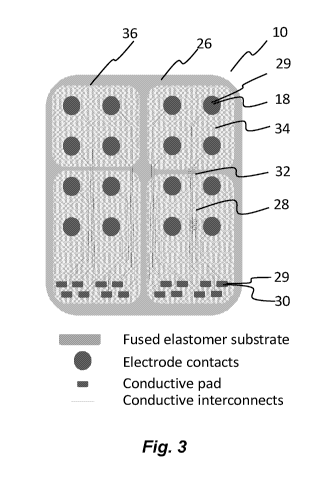
body. To that end, Figure 3 schematically shows a plan view of an implantable,
multi-electrode array 10 configured with in accordance with illustrative
embodiments of the invention. As shown, the implantable multi-electrode array
10 (e.g., for neuromodulation, cardiac stimulation, cardiac mapping, neural
recording, etc.) has a fused, unitary, ultra-thin electrode substrate 26
fabricated
with a mechanical robustness that can better withstand its implanted
environment. In other words, the substrate 26 may be considered to be one
piece¨with no seams (as noted above). This substrate 26 also may be referred
to
as a "body 26."
CA 03043007 2019-05-06
WO 2018/085840
PCT/US2017/060408
Illustrative embodiments of the electrode array 10 include micro-scale
continuous conductive elements, such as electrode sites 18, interconnects 28,
conductive contacts 30, and strain relief features 32 that enable high-density
implantable therapy arrays 10. The multi-contact electrode array 10 may have a
.. small number of electrodes, or a large number of electrodes (e.g., greater
than 16
electrodes) within the noted singular, unitary, fused, ultra-thin substrate
26.
The electrode array 10 includes an electrode site 18 with a conductive
surface for delivering electrical stimulation to body tissue. The conductive
interconnects 28, within the substrate 26, transmit electrical current from
the
conductive contacts 30 to the electrode sites 18, which also may provide the
interface/bonding sites to the lead 14 (Figure 2). Elastomeric material 34
electrically insulates the conductive interconnect 28, conductive contacts 30,
and
the body tissue to prevent short circuits and ensure that unintended
electrical
current does not leak into or otherwise interact in an unintended manner with
the body tissue. To improve robustness, the interconnect 28 may be configured
in
a serpentine pattern to form the noted strain relief features 32, enabling the
interconnects 28 to flex when subjected to certain expected forces (e.g., a
longitudinal force exerted on the electrode array 10).
In accordance with illustrative embodiments and as noted below, a
.. reinforcing material 36 (Figs 6A and 6B, discussed below) embedded within a
base and/or cover elastomer layer mechanically strengthens the electrode array
substrate assembly 26 without increasing rigidity or appreciable thickness.
Among other things, this reinforcing material 36 includes open areas, pores,
strips, or apertures to allow elastomers to continuously encapsulate (e.g.,
micro-
fiber, woven mesh, honeycomb, carbon fiber).
Illustrative embodiments form the substrate 26 by fusing at least one
discrete upper elastomer layer 34 (referred to as a "cover" or a "cover
layer") and
11
CA 03043007 2019-05-06
WO 2018/085840
PCT/US2017/060408
at least one discrete lower elastomer layer 34 (referred to as a "base" or a
"base
layer"). As discussed below with regard to Figure 11, the elastomer layers 34
are
prepared and spatially patterned in an unvulcanized material state, enabling
subsequent elastomer fusion to form the single, unitary (i.e., integral,
integrated,
etc.) substrate 26 containing conductive elements. This fused substrate 26
overcomes delamination failure modes experienced between adhesively-joined
layers of conventional approaches. As such, the unvulcanized material exists
in
the uncured, partially-cured, or "wet" state in which the material retains the
ability to be formed or joined. Among other things, the unvulcanized material
may include elastomers (e.g., silicone), polyurethanes (e.g., Pellethane,
Tecothane) or other polymers. As an example, the unvulcanized material may
include the first and second unvulcanized layers comprise thermoplastic
polyurethane. When vulcanized (discussed below), the two layers together form
a thermoplastic-polyurethane bond. In illustrative embodiments, the process
chemically bonds the base and cover together.
The electrode sites 18 and interconnects 28 preferably are formed from a
thin, continuous conductor material, such as a substantially flat, thin
continuous
metal conductor layer (e.g., a metal film or metal foil), with insulating
elastomer
material 34 on each side of the continuous conductive elements. For additional
robustness, the continuous conductive elements may contain anchor features,
such as slits, hooks, or holes, enabling insulating elastomer layers 34 to
anchor
the continuous conductive elements to the elastomer.
To further increase the number of electrode sites 18 and their density, the
electrode array substrate 26 also may include more than one layer of
continuous
conductive elements. For example, the substrate 26 may have two continuous
conductive element layers and three elastomer layers, increasing the contact
density. In a manner similar to other embodiments, this embodiment also has a
12
CA 03043007 2019-05-06
WO 2018/085840
PCT/US2017/060408
unitary, fused substrate 26 and optionally may have a reinforcement
material/layer 36 to improve its mechanical properties without increasing its
rigidity or appreciable thickness.
In illustrative embodiments, the continuous conductive elements are
formed from metal, such as a metal film or a metal sheet (e.g., foil). Other
embodiments, however, may form the continuous conductive elements from a
conductive polymer, or a hybrid material. Several examples of hybrid materials
may include a polymer having internal metal, carbon nanotubes, conductive ink,
conductive epoxy, or other conductive materials.
io The
array 10 may be arranged in any of a variety of different form factors.
For example, Figure 4 shows one implementation in which the electrode array 10
is arranged in a paddle configuration/assembly 38. As with some other
embodiments, this paddle assembly 38 has continuous conductive element
electrode sites 18 and conductor interconnects 28, and the lead 14 is
permanently
attached to the paddle assembly 38.
Figure 5 schematically compares a prior art adhesively bonded substrate
assembly against the unitary, fused substrate 26 of illustrative embodiments.
As
shown, the adhesively bonded substrate has two distinct layers 40 and 42 that
intersect/bond at an interface or seam 44. The fusion bonded substrate 26 of
Figure 5, however, is a single structure with no seams 44 (e.g., a continuous
transition of material).
Figures 6A 6B, and 6C schematically show cross-sectional views of a
fusion bonded substrate 26 configured in accordance with illustrative
embodiments of the invention. Figures 6A shows the substrate 26 as having
openings/apertures 29 both on its top and bottom surface, while Figures 6B and
6C show the substrate 26 as having openings/apertures 29 only on one surface.
13
CA 03043007 2019-05-06
WO 2018/085840
PCT/US2017/060408
Figure 6A and 6B also show the substrate having a reinforcement material
whereas Figure 6C does not contain a reinforcement material.
Additionally, to improve resilience to mechanic stress, illustrative
embodiments of Figures 6A and 6B include one or more types of polymer
reinforcement materials 36 within the substrate 26. To aid in protecting the
integrity of the device for an implanted environment, the reinforcing material
36
preferably has mechanical properties that are greater than that of the
elastomer
forming the substrate 26 and yet, do not increase rigidity or add appreciable
thickness. For example, the reinforcing material may contribute no more than
about 10 percent to the maximum total thickness. In some embodiments, the
reinforcing material 36 adds no net thickness because of its integration
within the
unitary body 26. When stretched, the polymer reinforcing material 36 is
proportionally strained, thereby preventing the conductors from solely
absorbing the strain.
Figure 7 shows one embodiment of the reinforcing material 36. As shown,
the reinforcing material 36 may be formed from one or multiple types of
materials (e.g., micro-fiber, woven mesh, honeycomb, carbon fiber) arranged as
an array of open areas. Accordingly, these open areas allow an elastomer to
contiguously permeate through the reinforcing material 36. The fibers
themselves preferably have a specified small fiber diameter (e.g., less than
500
micrometers diameter fibers). The right drawing of Figure 7 shows a close up
view of one implementation of the reinforcing material 36. Other embodiments
may not be woven as in Figure 7. For example, a layer with openings 29 may
suffice in certain applications. Those skilled in the art may form the form
the
reinforcing material 36 in other ways. For example, micro/nano-fibers could
also
be embedded within the elastomer to reinforce the substrate.
14
CA 03043007 2019-05-06
WO 2018/085840
PCT/US2017/060408
To accomplish its function, the reinforcing material 36 preferably has
material properties tuned to those of the unitary body 26. In illustrative
embodiments, the reinforcing material 36 has a tensile strength that is
greater
than that of the unitary body 26. In related embodiments, the reinforcing
material 36 has a tear strength that is greater than that of the unitary body
26.
Those skilled in the art may configure the body 26 and the reinforcing
material
36 to have one or more of these or other relative material properties (e.g.,
elongation).
As noted above, the electrode array 10 may take on a number of different
form factors. For example, Figure 8 schematically shows an illustrative
embodiment of the electrode array 10 taking on the form of a nerve cuff
therapy
electrode array (e.g., a cuff or spiral electrode array). As with other
embodiments, this embodiment has continuous conductive elements of
interconnects 28 and electrode sites 18. In use, this form factor may wrap
around
.. a nerve so that the electrodes electrode sites 18 face inwardly toward the
peripheral nerve fibers. The continuous conductive elements, which includes
electrode sites 18 and interconnects 28, are specifically formed to create the
conformal geometry around a nerve.
Figures 9A and 9B show other form factors. Specifically, Figure 9A
schematically shows a cylindrical electrode therapy array 10 having continuous
conductive elements, including electrode sites 18 and interconnects 28, which
have been curved to create the desired cylindrical geometry. The electrical
electrode sites 18 face outwardly for delivering therapy to a volume of
tissue.
The lead 14 preferably contains helically coiled conductors connected at the
conductive contacts 30 to the multi-contact therapy electrode array 10.
Figure 9B schematically shows a related embodiment in which the high-
density cylindrical electrode array 10 has continuous conductive elements with
CA 03043007 2019-05-06
WO 2018/085840
PCT/US2017/060408
electrode sites 18 and interconnects 28 that have been curved to create a
similar
cylindrical geometry. In a manner similar to the embodiment of Figure 9A, the
high-density electrical electrode sites 18 face outwardly for delivering
therapy to
a volume of tissue. The lead 14 contains helically coiled conductors connected
at
.. the conductive contacts 30 to the multi-contact therapy array 10.
Some embodiments may integrate active or passive electronics into the
electrode array 10 (e.g., switching electronics, components making to improve
systemic tolerance to magnetic resonant imaging, etc.). To that end, Figure 10
schematically shows the high-density paddle assembly 38 with its conductive
electrode sites 18 and interconnects 28 formed to create the planar geometry
as a
paddle assembly 38. Unlike prior embodiments, this paddle assembly 38 also
has an active electronics circuit module 48 connected to the continuous
conductive elements for switching current flow to the individual electrode(s).
The lead 14 contains helically coiled conductors that are connected at the
conductive contacts 30 to the electrode array 10. Note that other embodiments
also may have the active electronics circuit module 48. Alternatively, the
module
48 can have passive circuitry in addition to or instead of active circuitry.
In some
embodiments, rather than being in one location, the circuitry of the module 48
may be distributed across the electrode array 10.
Indeed, illustrative embodiments may use other form factors not
discussed. Accordingly, discussion of specific form factors, such as the noted
paddle and cylindrical form factors, are illustrative and not intended to
limit
additional embodiments.
Figure 11 shows a process of forming the above noted electrode array 10
.. in accordance with illustrative embodiments of the invention. It should be
noted
that this process is substantially simplified from a longer process that
normally
would be used to form the electrode array 10. Accordingly, the process of
16
CA 03043007 2019-05-06
WO 2018/085840
PCT/US2017/060408
forming the electrode array 10 may have many other steps, such as testing
steps
or etching steps, which those skilled in the art may use. In addition, some of
the
steps may be performed in a different order than that shown, or at the same
time.
Those skilled in the art therefore can modify the process as appropriate.
Moreover, as noted above and below, many of the materials and structures noted
are but one of a wide variety of different materials and structures that may
be
used. Those skilled in the art can select the appropriate materials and
structures
depending upon the application and other constraints. Accordingly, discussion
of specific materials and structures is not intended to limit all embodiments.
io To help understand Figure 11, Figure 12 schematically shows some of the
steps of the process of Figure 11. In fact, Figures 13 and 14 also
schematically
show some of the processes used to complete some of the steps in Figure 11.
The process of Figure 11 begins at step 1100, which forms the base layer.
To that end, Figure 13 schematically shows a process of forming a base layer
in
accordance with illustrative embodiments of the invention. As shown at step
(i)
of Figure 13, an ultra-thin elastomer substrate layer may be deposited on a
sacrificial/carrier substrate 50 in an unvulcanized state. Then, as shown at
(ii),
the unvulcanized elastomer substrate layer may be processed, such as by using
a
laser to cut or form openings 29, recesses and/or other features. For example,
.. those features may include the perimeter shape and curvature, holes to
expose
conductor electrode sites 18 to tissue, and holes to facilitate lead wires or
feed-
throughs. They also may include a feature outline, openings 29 for electrodes,
and alignment holes. In preferred embodiments, a patterning process (e.g., a
spatial patterning process, such as laser ablation) cuts the openings 29 while
the
.. elastomer layer is in an unvulcanized state. Elastomer material residuals
not
removed by the laser-patterning process may be manually removed (step iii). In
17
CA 03043007 2019-05-06
WO 2018/085840
PCT/US2017/060408
alternative embodiments, after vulcanization, the process may form the
openings
29, holes, apertures, etc.
After the elastomer residuals are removed from the assembly, the
assembly forms an unvulcanized, patterned elastomer base layer. The openings
.. 29 and recesses in the elastomer provide a conductive path for the
electrical
stimulation energy to pass from the electrode sites 18 to the tissue. The
openings
29 have rims that are just above the top surfaces of the electrode sites 18.
Thus,
the electrode sites 18 are slightly recessed relative to the rims of the
openings 29.
Optionally, the unvulcanized elastomer substrate 26 may include the
noted reinforcing material 36, which also is shown in Figure 13. As shown, the
reinforcement material 36 may be added at step (i) of Figure 13. Figure 14
shows
a similar process of forming the base layer, but without a reinforcing
material 36.
Returning to Figure 11, step 1102 also may form the cover layer. In a
manner similar to the base layer, the cover layer also may be formed in an
unvulcanized state and processed in a similar manner, either with or without
the
reinforcement material 36. Indeed, those skilled in the art can form the cover
layer using a number of other techniques.
Next, the process continues to step 1104, which forms the continuous
conductive elements. In this example, these elements are formed from a
flat/planar layer of metal. In other embodiments, however, other materials may
suffice, such as a conductive polymer, a non-flat metal layer, etc. Those
skilled in
the art thus can apply other materials to form the continuous conductive
elements. To those ends, Figure 15 schematically shows a process of forming
the
continuous conductive elements from a metal layer in accordance with
illustrative embodiments of the invention. The continuous conductive element
material may have a thickness of 5-50 micrometers and comprise primarily a
metal (e.g., platinum, platinum-iridium, palladium).
18
CA 03043007 2019-05-06
WO 2018/085840
PCT/US2017/060408
As shown in Figure 15, the continuous conductor (e.g., foil, strips, etc.)
may be applied to a sacrificial release carrier substrate 50, such as a
thermal
release or UV release carrier substrate 50 (step a, Figure 15). Step b of
Figure 15
then patterns the conductor (e.g.,. laser micro-machining or ablation) to form
continuous conductive elements, such as the electrode sites 18, conductive
interconnects 28, and conductive contacts 30. Accordingly, illustrative
embodiments form high-density continuous conductive elements (e.g., 25
micrometers lines with 25 micrometers spaces or larger) to produce multi-
contact
electrode arrays 10 (e.g., more than 16 electrodes 18).
Those skilled in the art may use other spatial patterning technologies,
such as film printing, screen printing, deposition or other method(s). Step
(c) of
Figure 15 then mechanically removes residual conductive elements 52, if
necessary, to achieve the desired continuous conductive elements spatially
arranged on the sacrificial release carrier substrate 50. Indeed, as noted
above,
the electrode array components may be formed from other materials that
perform the same functions and thus, discussion of specific materials and
thicknesses is not intended to limit the scope of various embodiments. For
example, other embodiments may use additive deposition processes with a
conductive polymer, ink, or some other conductor.
Returning to Figure 11, after forming the unvulcanized base,
unvulcanized cover, and continuous conductive elements, the process may begin
to assemble the overall unitary electrode body. To that end, step 1106
positions
and aligns the metal layer on the base layer, and step 1108 removes the
carrier
substrate 50 from the metal layer. Figure 12(ii) and (iii) graphically show
this
alignment, which preferably aligns the metal with appropriate openings 29,
among other things. Alternatively, other embodiments may align the conductive
element layer with the cover layer.
19
CA 03043007 2019-05-06
WO 2018/085840
PCT/US2017/060408
Next, step 1110 positions and aligns the metal layer with openings 29 in
the cover layer, while step 1112 removes the cover layer carrier substrate 50.
Figure 12 shows these two steps at (iv) and (v). Other embodiments may add
additional unvulcanized layers with and/or without flat reinforcement material
36, and additional layers of continuous conductive elements. Accordingly,
instead of just a single base and cover layer to be fused, the process may
repeat
some or all of the prior steps to add further unvulcanized layers with or
without
reinforcement material 36 and/or continuous conductive elements.
At this point in the process, the base and cover are ready to be fused
together to form the single, integral/unitary electrode substrate/body 26 as
discussed above. Specifically, step 1114 vulcanizes the assembly to create a
permanent elastomer fusion (elastomer-to-elastomer welding), forming the
single substrate 26. This involves applying heat and pressure, as required by
the
materials and application, to fuse the layers together. Among other benefits,
the
fusion process (v) is expected to provide electrical isolation and implanted
electrode longevity. The resulting metal contacts 30 and electrode sites 18
thus
are exposed as desired, although they may be recessed slightly below the rims
of
the openings 29 exposing them.
After completing the process, the fused unitary body 26 may be subjected
to various post-processing steps, such as step (vi), which may form the
electrode
therapy embodiments discussed above (among others) using a curving process
to form a curved electrode, cylindrical catheter electrode, nerve-cuff,
conformal
paddle, or other geometries. The sub-assembly from (v) therefore may be
combined with other processes that those skilled in the art may use to form
these
noted implementations. For example, to form a nerve cuff electrode or a
cylindrical catheter style electrode, the substrate 26 can be formed around a
CA 03043007 2019-05-06
WO 2018/085840
PCT/US2017/060408
mandrel and integrated with other injection molding or centerless grinding
steps.
Similarly, the post-processing step (vi) can attach wires from the lead 14 to
the contact contacts 30. Among other things, step (iv) can include various
types
of welding (e.g., thermo compression, resistance welding, laser welding,
conductive elastomers, etc.). The welding sites and exposed contact contacts
30
preferably are subsequently molded with thick elastomer insulating encapsulant
to provide isolation between the contact contacts 30.
Accordingly, unlike electrode arrays having bodies formed from two or
more adhered layers, illustrative embodiments form a unitary single body 26.
As
a result, the electrode array 10 should be more robust, particularly when
subjected to anticipated forces within the human body.
Although the above discussion discloses various exemplary embodiments
of the invention, it should be apparent that those skilled in the art can make
various modifications that will achieve some of the advantages of the
invention
without departing from the true scope of the invention.
21