Note: Descriptions are shown in the official language in which they were submitted.
1
CHEMFET ARRAY
This invention relates to improvements in or relating to the detection of
chemical and
biological reactions in an electrolyte solution, using semiconductor-based
devices;
specifically, Ion-Sensing Field Effect Transistors (ISFETS).
It is well known to provide an array of pixels for detecting chemical and
biological reactions.
The sensors used in such arrays are semiconductor devices and a great deal of
interest
and research has gone into the use of ISFET devices. ISFETs can be used to
measure
the hydrogen ion concentration or pH of an electrolyte solution. ISFETs are
popular
because they can be fabricated within a conventional Complementary Metal Oxide
Semiconductor (CMOS) technology, resulting in large array of pH sensors
alongside high
resolution data acquisition circuits.
In order to measure and record these reactions, it is well known to divide the
array into
columns of pixels and to provide an Analogue to Digital Converter (ADC) for
each column.
This is known as column parallel architecture and it has served the industry
well for many
years. The provision of a single ADC for each column reduces the hardware
requirement
as the ADC is configured to sample each of the pixels within a column, or
multiple columns,
.. sequentially thereby building up, over time, an output from each pixel.
It is against this background that the present invention has arisen.
According to the present invention there is provided an array of pixels,
wherein each pixel
comprises: a CHEMFET sensor; and an ADC. The CHEMFET sensor may be an ISFET
sensor.
The provision of an ADC within each pixel allows the analogue to digital
conversion to
take place within the pixel itself, rather than outside the pixel, as dictated
by the column
parallel architecture which forms the status quo within the technical field.
The provision of an ADC within each pixel allows simultaneous sampling of the
analogue
signal generated by all of the ISFETs within the array and conversion of this
into a digital
signal that can be output from each pixel.
Date Recue/Date Received 2023-09-19
CA 03043130 2019-05-07
WO 2018/083479
PCT/GB2017/053304
2
The provision of an ADC within each pixel means that space does not need to be
allocated on the chip for ADCs outside the sensor array. The provision of the
ADC within
each pixel effectively frees up space on the chip in comparison with column
parallel
architecture.
A further advantage of the provision of the ADC within the pixel, is that the
array is fully
scalable.
The ADC may be a sigma delta ADC, a SAR ADC, a Single-slope ADC, a dual-slope
ADC, a FLASH ADC or a pipelined ADC or a combination of the aforementioned
architectures. The ADC may be differential or single ended. The sigma delta
ADC may
be advantageous because it provides a higher resolution than other ADCs. A
sigma delta
ADC is also advantageous because it is an over sampling ADC and this sampling
is done
at a frequency much higher than the so-called "Nyquist" frequency, which is a
frequency
twice that of the signal bandwidth of interest. The technical effect of such a
high
frequency is that noise prior to the ADC sampling is effectively folded down
to lie with a
frequency range of 0 Hz to the half of the sampling frequency after sampling.
This noise,
together with the signal, then goes through a low pass decimation filter with
a cut-off
frequency of the signal bandwidth of interest and this filter thereby removes
almost all of
the noise.
This is in contrast with other types of ADC where the noise only folds down at
the lower
sample frequency, which is equal to the Nyquist frequency. As a result of this
all of the
noise is retained within the signal.
The sigma delta ADC may be a single ended first order sigma delta ADC which
has the
advantage of providing the smallest available architecture therefore enabling
the invention
to be implemented within the minimum possible area. A 1-bit first order sigma
delta ADC
particularly lends itself to incorporation within a pixel as all that is
required to facilitate the
operation of such an ADC is an amplifier, a comparator, a sample capacitor and
an
integration capacitor. The 1-bit first order sigma delta ADC does not require
any accurate
analog components such as transistors, resistors or capacitors. The required
components occupy a smaller silicon footprint than other ADCs. As a result,
the pixel size
is reduced in comparison with that which would be required to accommodate
other ADC
3
types. Therefore the pixel density is increased thereby providing more pixels
within a
fixed area.
Alternatively, the sigma delta ADC may be a second, third, fourth, fifth or
sixth order
sigma delta ADC.
Each pixel may further comprise bias control to control the amount of current
in the pixel.
The provision of the bias control within the pixel, rather than outside of the
pixel is for
noise control purposes as the positioning of the bias control within the pixel
prevents
noise from propagating from one pixel to the next through the bias control.
Each pixel may have an area in the region of 100pm x 100pm, or 50pm x 50pm or
25pm
x 25pm, or lOpm x lOpm or even 2.5pm x 2.5pm. The pixel may be square, or it
may be
rectangular. In order to increase the packing density of the pixels, hexagonal
pixels may
be used.
The array may comprise many pixels. There may be in the region of 4000 pixels,
or 6
million or even 100 million pixels. For example, the array may be 40x96 pixels
or
256x160. Because the pixels each include an ADC, they are fully scalable and
therefore
can be formed into an array of any practical size depending on the application
for which
the array will be used.
Each pixel may further comprise a switch configured to control the flow of
data from the
pixel onto a column on which each pixel is located.
Furthermore, according to another aspect, there is provided a chip comprising:
- an array of pixels wherein each pixel comprises: an ISFET sensor; and a
sigma
delta ADC, and
- a clocking arrangement comprising : a first clock signal common to all
pixels in the
array of pixels, for sampling an ISFET signal; and a second clock signal
provided
sequentially across the array of pixels, for conversion of the first clock
signal.
The provision of a first clock signal that is common to all of the pixels
enables the
simultaneous sampling of the analogue ISFET signal in each of the pixels.
The chip may be further configured to comprise control signals for each pixel
that enable
the ISFET and the ADC within each pixel to be switched on only when required.
This
Date Recue/Date Received 2023-09-19
CA 03043130 2019-05-07
WO 2018/083479
PCT/GB2017/053304
4
provides considerable reduction in the power required to operate the array and
consequent efficiency improvements in terms of unwanted heat within the array.
Furthermore, according to the present invention there is provided a device
comprising: an
array of wells each configured to receive a biological or chemical substance,
wherein the
array of wells is provided over a chip as discussed above.
This configuration provides considerable advantages over the column parallel
architecture
which forms the state of the art in this field, in that it enables the
sampling of the ISFET
signals from all pixels simultaneously. When the wells contain biological or
chemical
substances in which reactions may be taking place, the sampling of all of the
ISFET
signals at the same time ensures that the reactions taking place within the
wells are all at
the same point when the sample is taken. There is therefore no need to make
allowances
for differences in sample time when all of the samples have been taken at the
same time.
Once the sampling of all of the ISFETs has occurred simultaneously, then the
conversion
of the signal to a digital form may be staggered. If it is staggered then the
entire pixel
array is sampled at the same time whilst minimising the peak current
consumption of the
array.
The invention will now be further and more particularly described, by way of
example only,
and with reference to the accompanying drawings, in which:
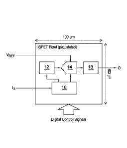
Figure 1 shows a pixel block diagram;
Figure 2 shows the connectivity of control signals and data output from an
exemplary four
pixels;
Figure 3 is a pixel timing diagram;
Figure 4 is an RVALID timing diagram; and
Figure 5 is a sigma delta ADC block diagram.
Figure 1 is a pixel block diagram showing a single 100pm square pixel 10 which
contains
CA 03043130 2019-05-07
WO 2018/083479
PCT/GB2017/053304
an ISFET 12, which is directly connected to a Sigma Delta ADC 14. The Sigma
Delta
ADC 14 is provided with ADC reference voltages VREF and is configured to
perform the
conversion of the analogue signal from the ISFET 12 into a digital bitstream.
5 The pixel 10 also includes bias control 16 which receives a bias current
IB from outside
the pixel 10. The bias current IB is in the region of 0.1pA to 100pA, for
example 2pA and
is used to provide bias control to the ISFET 12 and the Sigma Delta ADC 14.
The pixel 10 also includes a switch 18 which is configured to control the data
output 0
from the pixel 10. When the switch 18 is activated, it connects the data
output 0 from the
Sigma Delta ADC 14 to a column line which is provided outside the pixel 10.
Figure 2 shows the connectivity of the control signals and data output for an
exemplary
set of four pixels 10. For reasons of clarity, the bias control has been
omitted. The pixels
10 are each allocated a row and column number. The data outputs of all of the
pixels 10
in each column n, n+1, n+2 etc. are connected. Each row of pixels is
enumerated m,
m+1, m+2 etc. A switched capacitor implementation of a single-ended first
order sigma
delta modulator is used as the ADC. The ISFET 12 is a source follower NMOS
floating
gate transistor with its bulk tied to its source. In an alternative
embodiment, not illustrated
in the accompanying drawings, the single-ended first order sigma delta
modulator is
provided in a continuous time specification.
In the illustrated embodiment, the main control signals for the pixel 10 are:
CLK1, CLK2,
CLK3, PIX RSEL, SD_RSEL, and RVALID. CLK1 is used to sample the output from
all of
the ISFETs 12, while CLK2 and CLK3 are used to do the ADC conversion. PIX_RSEL
and SD_RSEL are the row enable signals for the ISFETs 12 and Sigma Delta ADCs
14,
respectively. The data from the SD ADC 14 is arranged in columns and is
controlled by
the corresponding RVALID signal, which indicates when data is valid on each
row. To
reduce power consumption, the pixels 10 are only turned on when needed.
One advantage of integrating the Sigma Delta ADC 14 into every pixel 10 is
that the entire
pixel array 100 can be sampled at the same time, therefore capturing the
output of all the
ISFETs 12 at the same point in time for every frame capture. This is a very
useful feature
for when it comes to processing the data, as allowances do not need to be made
for the
difference in time capture of the samples when a column parallel architecture
is used and
CA 03043130 2019-05-07
WO 2018/083479
PCT/GB2017/053304
6
the array is sampled row by row. To achieve simultaneous sampling of the
entire array
illustrated in Figure 2, CLK1 needs to be common to all the pixels. However,
as CLK2 and
CLK3 are only used to do the ADC conversion, they can be staggered between all
the
pixels 10 to reduce peak current consumption.
Figure 3 is a timing diagram of the control signals. The ISFETs 12 are all
sampled at the
same time via CLK1<39:0>. Subsequently, the analogue to digital conversion
takes place
in a staggered fashion via CLK2<39:0> and CLK3<39:0>. The only difference
between
CLK2<m> and CLK3<m> is that the falling edge of CLK3<m> occurs slightly before
the
falling edge of CLK2<m> (for simplicity, only CLK3<0> has been shown in Figure
3). The
pattern of CLK2 and CLK3 is repeated every 8th row as there is insufficient
time to
stagger all 40 rows within an oversampling period.
To reduce power consumption, the ISFET 12 and ADC 14 blocks within the pixels
10 are
only turned on when needed. This is achieved by turning on the corresponding
PIX RSEL
and SD_RSEL signals in advance of CLK1 and CLK2 respectively.
With reference to Figure 4, as there is only one data pin for every column,
RVALID is
used to latch the bitstream for each row of the pixel array to the output pin.
Data for each
pixel is only valid when RVALID is set high. RVALID_START is used to indicate
the start
of a new frame. All data collected within 2 RVALID_START pulses belong to the
same
frame.
When the RVALID signals for all the rows are LOW, the column data line is
pulled to
digital ground (GNDD) by a pull down resistor. This prevents the input to the
digital
controller from floating to an indeterminate voltage.
A block diagram of a single-ended first order sigma delta ADC is shown in
Figure 5. This
ADC is based on a switched capacitor network and operates at an oversampled
frequency of 30kHz. Assuming an oversampling ratio (OSR) of 512, the
downsampled
sample rate is thus just under 58.6Hz and the maximum signal bandwidth that
recovered
is no more than half that. In combination with a low-pass decimation filter
with a cut-off
frequency of the signal bandwidth of interest, this results in the noise
present before the
sampling being folded down and then effectively eliminated by the low-pass
decimation
filter.
CA 03043130 2019-05-07
WO 2018/083479
PCT/GB2017/053304
7
As will be apparent from Figure 5, the negative reference voltage is set to
the analogue
ground (GNDA) to reduce the number of signals going into the pixel 10. Both
the positive
reference voltage, VREFP, and the common mode reference voltage, VCM, are
buffered
within each pixel 10 to reduce noise coupling across the rows of pixels 10 in
the array
100.
It will further be appreciated by those skilled in the art that although the
invention has
been described by way of example with reference to several embodiments it is
not limited
to the disclosed embodiments and that alternative embodiments could be
constructed
without departing from the scope of the invention as defined in the appended
claims.