Note: Descriptions are shown in the official language in which they were submitted.
1
ANTENNAS AND DEVICES, SYSTEMS, AND METHODS INCLUDING THE SAME
CROSS REFERENCE TO RELATED APPLICATIONS
100011 The present application claims the benefits of and priority, under 35
U.S.C.
119(e), to U.S. Provisional Application Serial No. 62/712,778, filed on July
31, 2018, the
entire disclosure of which is hereby incorporated by reference, in its
entirety, for all that it
teaches and for all purposes.
FIELD
[0002] Example embodiments relate generally to antennas and devices, systems,
and
methods including the same.
BACKGROUND
[0003] Related art antennas (e.g., F-type antennas, patch antennas, etc.) have
limited
frequency bands and/or operating modes. Current solutions to these issues come
at the cost
of performance of the antenna (radiation efficiency, gain, etc.). Related art
antennas may also
require tuning and carefully controlled manufacturing processes in order to
achieve a desired
frequency band.
BRIEF DESCRIPTION OF THE DRAWINGS
[0004] Fig. 1 is a block diagram of a system according to at least one example
embodiment.
[0005] Fig. 2 illustrates a cross sectional view of an antenna structure
according to at least
one example embodiment;
[0006] Fig. 3 illustrates a first mode of the antenna structure in Fig. 2
according to at least
one example embodiment;
[0007] Fig. 4 illustrates a second mode of the antenna structure in Fig. 2
according to at
least one example embodiment;
[0008] Fig. 5 illustrates a cross sectional view of an antenna structure
according to at least
one example embodiment;
CA 3043418 2019-05-15
2
[0009] Fig. 6 illustrates a cross sectional view of an antenna structure
according to at least
one example embodiment;
[0010] Fig. 7 illustrates a cross sectional view of an antenna structure
according to at least
one example embodiment;
[0011] Fig. 8 illustrates a perspective view a system including an antenna
structure
according to at least one example embodiment;
[0012] Fig. 9A illustrates a plan view of an antenna structure according to at
least one
example embodiment. Fig. 9B illustrates a cross sectional view of the antenna
structure in
Fig. 9A;
[0013] Fig. 10 illustrates an example frequency bands for operating an antenna
structure in
a dual band mode according to at least one example embodiment; and
[0014] Fig. 11 illustrates an example frequency band for operating an antenna
structure in a
single band mode according to at least one example embodiment.
DETAILED DESCRIPTION
[0015] An antenna according to example embodiments allows for dual frequency
band
operation and a single wide band. This is achieved with a design that has
little or no effect on
antenna performance (gain, efficiency, etc.). For example, a T-antenna
according to example
embodiments has the ability to function in two distinct modes (e.g., even and
odd modes) of
resonant frequencies without modifying the structure of the antenna. The
frequencies of
those two modes can be controlled depending on design preferences. Depending
on the
frequency value of those modes, the T-antenna can either: resonate and
function in two
different frequency bands or combine those two modes in a single larger
frequency band not
possible with related art antenna designs.
[0016] The T-shaped concept can also be applied to patch antennas in order to
increase the
frequency bandwidth to a desired value. Benefits of the T-antenna dual
frequency bands
include improved radiation efficiency and improved return loss for the two
distinct band.
Additional benefits include that the T-antenna reduces process variation
problems ensures
that the desired frequency band is thoroughly covered, with margin to spare.
CA 3043418 2019-05-15
3
[0017] In view of the above and the following, it should be appreciated that
an antenna
according to example embodiments allows for the dual mode operation, each mode
with its
own distinctive frequency. By moving the frequencies of those modes (e.g., by
varying the
length of the short to ground), the antenna can be either: 1) dual band when
the frequencies of
the modes are quite far apart; or 2) single wide band when the frequencies of
those modes are
so close one to each other that they create a single wide band.
[0018] These and other needs are addressed by the various aspects,
embodiments, and/or
configurations of the present disclosure.
[0019] Fig. 1 is a block diagram of a system 100 according to at least one
example
embodiment. The system 100 includes a communication device 105 and an external
device
110 capable of communicating with one another over a wireless connection at
one or more
desired frequencies using one or more desired protocols (e.g., for near-field
communication
(NFC), Wi-Fi, BLUETOOTH, global position system (GPS), etc.). The
communication
device 105 and/or the external device 110 may be a mobile device such as a
smart phone, a
piece of wearable technology (e.g., a smart watch, a fitness band, etc.).
Additionally or
alternatively, the communication device 105 and/or the external device 110 may
be a
stationary device mounted to or placed on a surface, such as a smart
thermostat, or other
piece of smart home technology. In other words, the communication device 105
and the
external device 110 may be any two devices where wireless communication
between the
devices is desired.
[0020] The communication device 105 may include an antenna 115 and an
integrated
circuit (IC) 120 that processes signals received and/or sent by the antenna
115. For example,
when the antenna 115 is in the presence of the external device 110, the IC 120
may facilitate
two-way communication between the communication device 105 and the external
device 110
through the antenna 115. Although not explicitly shown, it should be
understood that the
external device 110 may include its own corresponding IC and antenna to
communicate with
the communication device 105. In this case, the external device 110 may have
the same IC
and the same antenna as the communication device 105. Details of the antenna
115 are
discussed below with reference to Figs. 2-8.
[0021] The communication device 105 and/or the external device 110 may be an
active
device or a passive device. If the communication device 105 and/or the
external device 110
CA 3043418 2019-05-15
4
is an active device, then a power source (e.g., a battery) may be included in
the respective
device for providing power to a respective IC. If the communication device 105
and/or the
external device 110 is a passive device, then the respective device does not
include a power
source and may rely on signals received at a respective antenna to power the
respective IC.
In at least one example embodiment, one of the communication device 105 or the
external
device 110 is an active device while the other of the communication device 105
or the
external device 110 is a passive device. However, example embodiments are not
limited
thereto, and both devices 105/110 may be active devices if desired.
[0022] The IC 120 may comprise one or more processing circuits capable of
controlling
communication between the communication device 105 and the external device
110. For
example, the IC 120 includes one or more of an application specific integrated
circuit (ASIC),
a processor and a memory (e.g., nonvolatile memory) including instructions
that are
executable by the processor, programmable logic gates, etc.
[0023] Fig. 2 illustrates a cross sectional view of an antenna structure 200A
for the antenna
115 of Fig. 1 according to at least one example embodiment.
[0024] As shown in Fig. 2, the antenna structure 200A may include a first
conductive
element (or antenna) 205. The first conductive element 205 includes a first
planar portion
210 having a length L, and an extension portion 215 that extends away from the
first planar
portion 210 at a center of the first planar portion 210. The center of the
first planar portion
210 may be an exact or near exact center of the first planar portion 210 in
both the x and y
directions (i.e., horizontal directions). Alternatively, the extension portion
215 may extend
away from the first planar portion 210 at a location offset from the center if
desired (e.g.,
according to design preferences). The antenna structure 200A may include a
second
conductive element 217 spaced apart from the first planar portion 210 by a
desired distance.
[0025] The extension portion 215 may have a length B. In Fig. 2, the desired
distance
between the second conductive element 217 and the first planar portion 210 and
the length of
the extension portion are both equal to B. However, example embodiments are
not limited
thereto, as further described below with reference to Figs. 6-7, for example.
[0026] In Fig. 2, the space between the first planar portion 210 and the
second conductive
element 217 is occupied by ambient air. The second conductive element 217 may
include a
second planar portion 220 electrically connected to the extension portion 215.
In at least one
CA 3043418 2019-05-15
5
example embodiment, the second planar portion 220 is a ground plate that is
connected to
electrical ground or a common voltage and that extends at least the length and
the width of
the first planar portion 210. However, example embodiments are not limited
thereto and
other configurations and/or dimensions of the second planar portion 220 may be
selected if
desired.
[0027] As shown in Fig. 2, the first planar portion 210 and the second planar
portion 220
extend in a first direction so as to be substantially parallel to one another.
The extension
portion 215 extends in a direction that is substantially perpendicular to the
first direction.
According to at least one example embodiment and as shown in Fig. 2, the
extension portion
215 is linear. However, example embodiments are not limited thereto and other
shapes of the
extension portion 215 may be possible as shown in Figs. 6, 7, and 9.
[0028] The length L and the distance B may be design parameters based on
empirical
evidence and/or preference (e.g., based on desired frequency band(s) for the
antenna). These
parameters are discussed in more detail below with reference to Figs. 3 and 4.
The first
conductive element 205 and the second conductive element 217 may comprise
copper or
other suitable conductive material used for antenna applications.
[0029] Fig. 2 illustrates an insulating material 225 that supports the second
planar section
225. The insulating material 225 may be a substrate, for example, a printed
circuit board
(PCB) or other insulative substrate that includes other elements of the
communication device
105 mounted thereto (e.g., the IC 120).
[0030] As shown in Fig. 2, the antenna structure 200A may further include an
injection port
230 coupled to a transmit/receive line 235. The injection port 230 may include
a conductive
strip of metal coupled to the first planar portion 210 and to the transmit
receive line 235. The
conductive strip of the injection port 230 that passes through at least the
second planar
portion 220 may be electrically insulated from the second planar portion 220,
for example, by
an insulating wrapper. The transmit/receive line 235 may be a conductive
wiring that leads to
the IC 120 so that the IC 120 can send and receive signals from the antenna
structure 200A.
In operation, the injection port 230 functions as an input/output port for the
antenna structure
200A. Fig. 2 shows that the injection port 230 is located close to the
extension portion 215,
however, example embodiments are not limited thereto and the injection port
230 may be
placed at some other location according to design preferences.
CA 3043418 2019-05-15
6
100311 Fig. 3 illustrates a first mode of the antenna structure 200A in Fig. 2
according to at
least one example embodiment. In more detail, Fig. 3 illustrates an odd
resonant mode for
the antenna structure 200A. The odd resonant mode may correspond to a mode in
which the
antenna structure 200A is operable in a first frequency bandwidth. As shown in
Fig. 3, the
odd resonant mode is symmetric (e.g., perfectly symmetric) and has a virtual
electric wall or
virtual ground plane) through the extension portion 215 such that no current
flows to the
ground plate 220 to create opposite phase electric fields E for each branch of
the first planar
portion 210. For each branch of the first planar portion 210, current travels
a distance of L/2
(which is considered a quarter wavelength). Thus, the wavelength X in the odd
resonant
mode Xo=2L. The resonant frequency Fo for the odd mode is Fo=cao, where c is
the speed
of light (e.g., in m/s). In at least one example embodiment, for example, in a
dual band mode
Fo=2.4GHz.
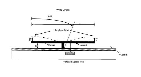
100321 Fig. 4 illustrates a second mode of the antenna structure 200A in Fig.
2 according to
at least one example embodiment. In more detail, Fig. 4 illustrates an even
resonant mode for
the antenna structure 200A. The even resonant mode may correspond to a mode in
which the
antenna structure 200A is operable in a second frequency bandwidth that is
distinct from the
first frequency bandwidth of the odd resonant mode in Fig. 3. As shown in Fig.
4, the even
resonant mode is symmetric (e.g., perfectly symmetric) and has a virtual
magnetic wall along
the extension portion 215 such that current in each branch of the first planar
portion 215
flows to the ground plate 220 through the extension portion 215 to create in-
phase electric
fields E for each branch. For each branch of the first planar portion 215, the
current travels a
distance of about a quarter wavelength ke/4 or about L/2 (e.g., slightly
greater than ke/4 or
L/2 because of the extension portion 215). Thus, the wavelength ke in the even
resonant
mode may be expressed as follows: ke-2L+4B. The resonant frequency Fe for the
even
mode is Fe=c/ke. In at least one example embodiment, for example, in a dual
band mode
Fe=1.7GHz.
[0033] In view of Figs. 3 and 4, it should be appreciated that ke> AD and that
Fe<Fo, which
may create two distinct frequency bands, one band for the odd resonant mode
and one band
for the even resonant mode. It should further be appreciated that the creation
of two distinct
frequency bands may be dependent on the distance B. For example, if the
distance B is
relatively large, then each resonant mode may have its own frequency band as
described
above. However, if the distance B is relatively small, then the frequency
bands of each
CA 3043418 2019-05-15
7
resonant mode may partially overlap to create a single frequency band that is
wider than
either of the two distinct frequency bands. In other words, the frequency
bands of the odd
resonant mode and the even resonant mode may be merged into a single enhanced
frequency
band. Figs. 6, 7, and 9-11 illustrate examples of adjusting the distance B
according to a
desired frequency band of the antenna structure.
[0034] Fig. 5 illustrates a cross sectional view of an antenna structure 200B
according to at
least one example embodiment. Fig. 5 is the same as Fig. 2 except for the
inclusion of an
insulating material 500 between the first planar portion 210 and the second
planar portion
220. As shown, the extension portion 215 passes through the insulating
material 500 to
electrically connect with the second planar portion 220. The insulating
material 500 may
comprise the same or different material as the insulating material 225. For
example, the
insulating material 500 may be a portion of a PCB or other suitable insulative
material used
in antenna applications. As also shown, the injection port 230 is disposed in
the insulating
material 225 and includes a conductive section that passes through the second
planar portion
220 and the insulating material 500 to electrically connect with the first
planar portion 210.
The conductive section of the injection port 230 that passes through at least
the second planar
portion 220 may be electrically insulated from the second planar portion 220,
for example, by
an insulating wrapper. As in Fig. 2, the injection port 230 is coupled to a
transmit/receive
line 235 of an integrated circuit 120 for the antenna structure 200B.
[0035] In Fig. 5, a top surface of the first planar portion 210 is coplanar
with a top surface
of the insulating material 500. However, example embodiments are not limited
thereto, and
the top surfaces may be offset from one another in either vertical direction.
[0036] Fig. 6 illustrates a cross sectional view of an antenna structure 200C
according to at
least one example embodiment. The antenna structure 200C is the same as the
antenna
structure 200B in Fig. 5, except that antenna structure 200C includes an
extension portion
215A that is sinuous or winding. This configuration may be useful for
applications where
dual frequency bands are desired because the sinuous structure of the
extension portion 215A
serves to increase the effective length B because the current path to the
ground plate 220 is
longer than in Fig. 5, for example. This creates an even resonant mode with a
frequency Fe
lower than Fo, and even lower than the frequency Fe from Fig. 5 if the
distance between
planar portions 210 and 220 is maintained. That is, as the sinuous path of the
extension
portion 215A lengthens, Fe decreases. Accordingly, a total length of the
extension portion
CA 3043418 2019-05-15
8
215A may be a design parameter set based on a desired resonant frequency Fe.
This
configuration allows for a dual band antenna mode while keeping the overall
package
compact (because the distance between the planar portions 210 and 220 need not
increase
from the configuration shown in Fig. 5). Here, it should be appreciated that
the sinuous
structure of the extension portion 215A does not affect the resonant frequency
Fo in the odd
resonant mode.
[0037] Fig. 7 illustrates a cross sectional view of an antenna structure 200D
according to at
least one example embodiment. The antenna structure 200D is the same as the
antenna
structure 200B in Fig. 5, except that antenna structure 200D includes an
extension portion
215B that includes a first part 700 and a second part 705 spaced apart from
the first part in
the first direction (e.g., a horizontal direction) so that a gap 710 exists
between two sections
or branches of the first planar portion 210. Here, the presence of the gap 710
may serve to
decrease the effective length B of the extension portion 215B compared to
extension portion
215 Fig. 5. Fig. 7 may be useful for applications that desire a single wide
bandwidth (e.g., at
10dB) that is otherwise not possible or ineffective for related art patch
and/or F-antenna
designs. The single frequency band of the antenna structure 200D may be
include and/or be
wider than either of the frequency bands accomplished by the even and odd
resonant modes
alone.
[0038] Fig. 8 illustrates a perspective view a system 800 including an antenna
structure
according to at least one example embodiment. In more detail, Fig. 8
illustrates how the
antenna structure 200A is mounted in a device 805. The device 805 may
correspond to the
communication device 105. For example, the device 805 may be a wearable
device, such as
a smart watch. Although Fig. 8 is described with respect to antenna structure
200A, it should
be appreciated that all antenna structures described herein and within the
scope of inventive
concepts may be included in addition to or instead of structure 200A.
[0039] Fig. 9A illustrates a plan view of an antenna structure 900 according
to at least one
example embodiment. Fig. 9B illustrates a cross sectional view of the antenna
structure 900
in Fig. 9A. The antenna structure 900 may be used in the antenna 115 of Fig.
1. In more
detail, Figs. 9A and 9B are similar to Figs. 2-7 in that the antenna structure
900 employs the
same T-antenna concept, but with a wider patch-like section 910 instead of
thinner T-tops as
in Fig. 8. With reference to Figs. 9A and 9B, the antenna structure 900
includes a substrate
905, a first conductive plate 907 (e.g., a ground plate) on the substrate 905,
a second
CA 3043418 2019-05-15
9
conductive plate 910 electrically connected to the first conductive plate 907
by a plurality of
conductive vias 915. An optional carrier substrate 908 may be included if
desired. Here, it
should be understood that the extension portions 215, 215A, and 215B of the
previous figures
are represented by the plurality of conductive vias 915 positioned in a row or
column at a
center of the conductive plate 907. That is, the extension portion of the
antenna structure 900
includes a plurality of conductive vias 905 aligned in a direction and that
extend from one
side of the first planar portion (e.g., 220 or 910) to an opposite side of the
first planar portion
(220 or 910).
[0040] The size, density, and/or position of the conductive vias 915 may
affect the effective
length of B. In at least one example embodiment, the conductive vias 915
function similar to
the extension portion 215B in that the effective length B is relatively short,
thereby creating a
single wide frequency band. For example, the more tightly packed the
conductive vias 915 in
a row, the shorter the effective length of B which brings Fe closer to Fo to
create a single
frequency band (e.g., at 10db).
[0041] In view of Figs. 1-9, it should be understood that at least one example
embodiment
is directed to an antenna structure including a ground plate 220 and an
antenna 205 having a
T-shape that includes a top 210 and a leg 215. The top 210 of the T-shape is
spaced apart
from the ground plate 220, and the leg 215 of the T-shape extends away from
the top 210 of
the T-shape and is electrically connected to the ground plate 220. The leg 215
of the T-shape
has a structure such that i) the antenna is operable for a first frequency
bandwidth and a
second frequency bandwidth distinct from the first frequency bandwidth, or ii)
the antenna is
operable for a single frequency bandwidth that is wider compared to the first
and second
frequency bandwidths taken alone.
[0042] In at least one example embodiment, the structure of the leg 215 of the
T-shape may
be a linear structure (e.g., in Fig. 5) having a length B that matches a
distance between the
ground plate 220 and the top 210 of the T-shape so that the antenna is
operable for the first
frequency bandwidth and the second frequency bandwidth.
[0043] In at least one example embodiment, the structure of the leg 215 of the
T-shape is a
sinuous structure (e.g., in Fig. 6) having a length B that is greater than a
distance between the
ground plate 220 and the top 210 of the T-shape so that the antenna is
operable for the first
frequency bandwidth and the second frequency bandwidth.
CA 3043418 2019-05-15
10
[0044] In at least one example embodiment, the structure of the leg 215 of the
T-shape is a
U-shaped structure (e.g., Fig. 7) that creates a gap 710 between two sections
or branches of
the top 210 of the T-shape so that the antenna is operable for the single
frequency bandwidth.
[0045] In at least one example embodiment, the structure of the leg 215 of the
T-shape
includes a plurality of conductive vias 915 aligned with one another so that
the antenna is
operable for the single frequency bandwidth.
[0046] According to at least one example embodiment, the antenna structure
includes a first
insulating material 500 between the top 210 of the T-shape and the ground
plate 220. Here,
the leg 215 of the T-shape passes through the first insulating material 500 to
electrically
connect with the ground plate 220. At least one example embodiment includes a
second
insulating material 225 that supports the ground plate 220.
[0047] The antenna structure may include an injection port 230 disposed in the
second
insulating material 225 and that includes a conductive section that passes
through the ground
plate 220 and the first insulating material 500 to electrically connect with
the top 210 of the
T-shape. The injection port 230 is coupled to a transmit/receive line 235 of
an integrated
circuit 120 for the antenna structure.
[0048] Fig. 10 illustrates an example frequency bands for operating an antenna
structure in
a dual band mode in accordance with at least one example embodiment. As shown
in Fig. 10,
the antenna structure operating in an even resonant mode and an odd resonant
mode creates
two distinct frequency bands so as to allow a single antenna to operate in
multiple bands.
[0049] Fig. 11 illustrates an example frequency band for operating an antenna
structure in a
single band mode in accordance with at least one example embodiment. As may be
appreciated from a comparison of Figs. 10 and 11, operating the antenna
structure according
to example embodiments in a single band mode achieves a single wide frequency
band that
includes at least part of the frequency bands of the odd and even resonant
modes and that is
wider than either of the frequency bands for the odd resonant mode or the even
resonant
mode taken alone, for example, at 10dB.
[0050] In view of Figs. 1-11, it should be understood that example embodiments
may
include a method that includes operating a T-shaped antenna in a first mode
and a second
mode. The first mode is a mode in which the T-shaped antenna has a first
resonant
CA 3043418 2019-05-15
11
frequency (e.g., Fe) and a first frequency bandwidth, as well as a second
resonant frequency
(e.g., Fo) distinct from the first resonant frequency and a second frequency
bandwidth distinct
from the first frequency bandwidth. The second mode is a mode in which the
antenna has an
expanded frequency bandwidth (e.g., see Fig. 11) that may include the first
and second
frequency bandwidths of first mode. For example, the expanded frequency
bandwidth covers
a larger range of frequencies than the first mode and the second mode alone.
Selection of the
first mode or the second mode may be a design choice. In at least one example
embodiment,
a single antenna may be capable of operating in the first mode, for example,
when B is a
relatively large value. That is, a single antenna can transmit and receive
effectively within
two different frequency bands to allow communication within, for example, both
GPS and
WiFi frequency bands (at about 1.5GHz and 2.44 GHz, respectively). If B is a
relatively
small value, then the antenna may operate in the second mode to achieve an
enhanced
frequency bandwidth compared to the first mode. Although not explicitly shown,
it should be
understood that the value of B may be adjustable by lengthening or shortening
the extension
portion 215. For example, the extension portion 215 may exist in segments with
at least one
of the segments being attached to one or more mechanisms that move (e.g.,
horizontally
move) a respective segment in or out of alignment with other segments of the
extension
portion 215 electrically connected to the planar portion 210. Here, the
substrate 225 may also
be attached to one or more mechanisms so as to be movable in a vertical
direction (e.g.,
further away from or closer to the extension portion 215) to allow for the
exchange of
extension portion segments and then re-connection. In view of the above, it
should be
appreciated that example embodiments provide a single antenna or resonator
with multiple
possible operating modes while maintaining high levels of radiation
efficiency, desirable
radiation pattern, high gain, improved bandwidth, etc.
[0051] Although example embodiments have been described with reference to
specific
elements in the figures, it should be understood that elements of some
embodiments may be
added or removed to/from other embodiments if desired.
[0052] According to at least one example embodiment, an antenna structure
includes a first
conductive element including a first planar portion, and an extension portion
that extends
away from the first planar portion at a center of the first planar portion.
The antenna structure
may include a second conductive element spaced apart from the first planar
portion and
electrically connected to the extension portion.
CA 3043418 2019-05-15
12
[0053] According to at least one example embodiment, the second conductive
element
includes a second planar portion, the first planar portion and the second
planar portion extend
in a first direction so as to be substantially parallel to one another, and
the extension portion
extends in a direction that is substantially perpendicular to the first
direction.
[0054] According to at least one example embodiment, the extension portion is
linear.
[0055] According to at least one example embodiment, the extension portion is
sinuous.
[0056] According to at least one example embodiment, the extension portion
includes a
first part and a second part spaced apart from the first part in the first
direction so that a gap
exists between two sections of the first planar portion.
[0057] According to at least one example embodiment, the extension portion
includes
separable segments.
[0058] According to at least one example embodiment, the extension portion
includes a
plurality of conductive vias aligned in the first direction and that extend
from one side of the
first planar portion to an opposite side of the first planar portion.
[0059] According to at least one example embodiment, the antenna structure
includes a first
insulating material between the first planar portion and the second conductive
element. The
extension portion passes through the first insulating material to electrically
connect with the
second conductive element.
[0060] According to at least one example embodiment, the antenna structure
includes a
second insulating material that supports the second conductive element.
[0061] According to at least one example embodiment, the antenna structure
includes an
injection port disposed in the second insulating material and includes a
conductive section
that passes through the second conductive element and the first insulating
material to
electrically connect with the first planar portion. The injection port is
coupled to a
transmit/receive line of an integrated circuit for the antenna structure.
[0062] According to at least one example embodiment, the second conductive
element is
grounded.
CA 3043418 2019-05-15
13
[0063] According to at least one example embodiment, an antenna structure
includes a
ground plate, and an antenna having a T-shape that includes a top and a leg.
The top of the
T-shape is spaced apart from the ground plate, and the leg of the T-shape
extends away from
the top of the T-shape and is electrically connected to the ground plate. The
leg of the T-
shape has a structure such that i) the antenna is operable for a first
frequency bandwidth and a
second frequency bandwidth distinct from the first frequency bandwidth, or ii)
the antenna is
operable for a single frequency bandwidth that is wider compared to the first
and second
frequency bandwidths taken alone.
[0064] According to at least one example embodiment, the structure of the leg
of the T-
shape is a linear structure having a length that matches a distance between
the ground plate
and the top of the T-shape so that the antenna is operable for the first
frequency bandwidth
and the second frequency bandwidth.
[0065] According to at least one example embodiment, the structure of the leg
of the T-
shape is a sinuous structure having a length that is greater than a distance
between the ground
plate and the top of the T-shape so that the antenna is operable for the first
frequency
bandwidth and the second frequency bandwidth.
[0066] According to at least one example embodiment, wherein the structure of
the leg of
the T-shape is a U-shaped structure that creates a gap between two sections of
the top of the
T-shape so that the antenna is operable for the single frequency bandwidth.
[0067] According to at least one example embodiment, the structure of the leg
of the T-
shape includes a plurality of conductive vias aligned with one another so that
the antenna is
operable for the single frequency bandwidth.
[0068] According to at least one example embodiment, the antenna structure
includes a first
insulating material between the top of the T-shape and the ground plate, and
the leg of the T-
shape passes through the first insulating material to electrically connect
with the ground plate.
[0069] According to at least one example embodiment, the antenna structure
includes a
second insulating material that supports the ground plate.
[0070] According to at least one example embodiment, the antenna structure
includes an
injection port disposed in the second insulating material and includes a
conductive section
CA 3043418 2019-05-15
14
that passes through the ground plate and the first insulating material to
electrically connect
with the top of the T-shape. he injection port being coupled to a
transmit/receive line of an
integrated circuit for the antenna structure.
[0071] According to at least one example embodiment, an antenna includes a
ground plate
and a T-shaped antenna structure in electrical contact with the ground plate
and configured to
operate in a first mode or a second mode. The first mode is a mode in which
the T-shaped
antenna structure is operable in a first frequency bandwidth and a second
frequency
bandwidth distinct from the first frequency bandwidth, and the second mode is
a mode in
which the T-shaped antenna structure is operable in an expanded frequency
bandwidth that
includes the first frequency bandwidth and the second frequency bandwidth.
[0072] The phrases "at least one", "one or more", "or", and "and/or" are open-
ended
expressions that are both conjunctive and disjunctive in operation. For
example, each of the
expressions "at least one of A, B and C", "at least one of A, B, or C", "one
or more of A, B,
and C", "one or more of A, B, or C", "A, B, and/or C", and "A, B, or C" means
A alone, B
alone, C alone, A and B together, A and C together, B and C together, or A, B
and C
together.
[0073] The term "a" or "an" entity refers to one or more of that entity. As
such, the terms
"a" (or "an"), "one or more" and "at least one" can be used interchangeably
herein. It is also
to be noted that the terms "comprising", "including", and "having" can be used
interchangeably.
[0074] The term "automatic" and variations thereof, as used herein, refers to
any process or
operation, which is typically continuous or semi-continuous, done without
material human
input when the process or operation is performed. However, a process or
operation can be
automatic, even though performance of the process or operation uses material
or immaterial
human input, if the input is received before performance of the process or
operation. Human
input is deemed to be material if such input influences how the process or
operation will be
performed. Human input that consents to the performance of the process or
operation is not
deemed to be "material".
[0075] The term "computer-readable medium" or "memory" as used herein refers
to any
computer-readable storage and/or transmission medium that participate in
providing
instructions to a processor for execution. Such a computer-readable medium can
be tangible,
CA 3043418 2019-05-15
15
non-transitory, and non-transient and take many forms, including but not
limited to, non-
volatile media, volatile media, and transmission media and includes without
limitation
random access memory ("RAM"), read only memory ("ROM"), and the like. Non-
volatile
media includes, for example, NVRAM, or magnetic or optical disks. Volatile
media includes
dynamic memory, such as main memory. Common forms of computer-readable media
include, for example, a floppy disk (including without limitation a Bernoulli
cartridge, ZIP
drive, and JAZ drive), a flexible disk, hard disk, magnetic tape or cassettes,
or any other
magnetic medium, magneto-optical medium, a digital video disk (such as CD-
ROM), any
other optical medium, punch cards, paper tape, any other physical medium with
patterns of
holes, a RAM, a PROM, and EPROM, a FLASH-EPROM, a solid state medium like a
memory card, any other memory chip or cartridge, a carrier wave as described
hereinafter, or
any other medium from which a computer can read. A digital file attachment to
e-mail or
other self-contained information archive or set of archives is considered a
distribution
medium equivalent to a tangible storage medium. When the computer-readable
media is
configured as a database, it is to be understood that the database may be any
type of database,
such as relational, hierarchical, object-oriented, and/or the like.
Accordingly, the disclosure
is considered to include a tangible storage medium or distribution medium and
prior art-
recognized equivalents and successor media, in which the software
implementations of the
present disclosure are stored. Computer-readable storage medium commonly
excludes
transient storage media, particularly electrical, magnetic, electromagnetic,
optical, magneto-
optical signals.
[0076] A computer readable signal medium may be any computer readable medium
that is
not a computer readable storage medium and that can communicate, propagate, or
transport a
program for use by or in connection with an instruction execution system,
apparatus, or
device. A computer readable signal medium may convey a propagated data signal
with
computer readable program code embodied therein, for example, in baseband or
as part of a
carrier wave. Such a propagated signal may take any of a variety of forms,
including, but not
limited to, electro-magnetic, optical, or any suitable combination thereof.
Program code
embodied on a computer readable signal medium may be transmitted using any
appropriate
medium, including but not limited to wireless, wireline, optical fiber cable,
RF, etc., or any
suitable combination of the foregoing.
CA 3043418 2019-05-15
16
[0077] The terms "determine", "calculate" and "compute," and variations
thereof, as used
herein, are used interchangeably and include any type of methodology, process,
mathematical
operation or technique.
[0078] The term "means" as used herein shall be given its broadest possible
interpretation
in accordance with 35 U.S.C., Section(s) 112(f) and/or 112, Paragraph 6.
Accordingly, a
claim incorporating the term "means" shall cover all structures, materials, or
acts set forth
herein, and all of the equivalents thereof. Further, the structures, materials
or acts and the
equivalents thereof shall include all those described in the summary, brief
description of the
drawings, detailed description, abstract, and claims themselves.
[0079] The term "module" as used herein refers to any known or later developed
hardware,
software, firmware, artificial intelligence, fuzzy logic, or combination of
hardware and
software that is capable of performing the functionality associated with that
element.
[0080] Examples of the processors as described herein may include, but are not
limited to,
at least one of Qualcomm Snapdragon 800 and 801, Qualcomm Snapdragon 610
and
615 with 4G LTE Integration and 64-bit computing, Apple A7 processor with 64-
bit
architecture, Apple M7 motion coprocessors, Samsung Exynos series, the
Intel
CoreTM family of processors, the Intel Xeon family of processors, the Intel
AtomTM
family of processors, the Intel Itaniume family of processors, Intel Core i5-
4670K and
i7-4770K 22nm Haswell, Intel Core i5-3570K 22nm Ivy Bridge, the AMD FXTM
family
of processors, AMD FX-4300, FX-6300, and FX-8350 32nm Vishera, AMD Kaveri
processors, Texas Instruments Jacinto C6000TM automotive infotainment
processors, Texas
Instruments OMAPTm automotive-grade mobile processors, ARM CortexTMM
processors, ARM Cortex-A and ARM926EJ-STm processors, other industry-
equivalent
processors, and may perform computational functions using any known or future-
developed
standard, instruction set, libraries, and/or architecture.
[0081] Any of the steps, functions, and operations discussed herein can be
performed
continuously and automatically.
[0082] Although the present disclosure describes components and functions
implemented
in the aspects, embodiments, and/or configurations with reference to
particular standards and
protocols, the aspects, embodiments, and/or configurations are not limited to
such standards
and protocols. Other similar standards and protocols not mentioned herein are
in existence
CA 3043418 2019-05-15
17
and are considered to be included in the present disclosure. Moreover, the
standards and
protocols mentioned herein and other similar standards and protocols not
mentioned herein
are periodically superseded by faster or more effective equivalents having
essentially the
same functions. Such replacement standards and protocols having the same
functions are
considered equivalents included in the present disclosure.
[0083] The present disclosure, in various aspects, embodiments, and/or
configurations,
includes components, methods, processes, systems and/or apparatus
substantially as depicted
and described herein, including various aspects, embodiments, configurations
embodiments,
subcombinations, and/or subsets thereof. Those of skill in the art will
understand how to
make and use the disclosed aspects, embodiments, and/or configurations after
understanding
the present disclosure. The present disclosure, in various aspects,
embodiments, and/or
configurations, includes providing devices and processes in the absence of
items not depicted
and/or described herein or in various aspects, embodiments, and/or
configurations hereof,
including in the absence of such items as may have been used in previous
devices or
processes, e.g., for improving performance, achieving ease and\or reducing
cost of
implementation.
[0084] The foregoing discussion has been presented for purposes of
illustration and
description. The foregoing is not intended to limit the disclosure to the form
or forms
disclosed herein. In the foregoing Detailed Description for example, various
features of the
disclosure are grouped together in one or more aspects, embodiments, and/or
configurations
for the purpose of streamlining the disclosure. The features of the aspects,
embodiments,
and/or configurations of the disclosure may be combined in alternate aspects,
embodiments,
and/or configurations other than those discussed above. This method of
disclosure is not to
be interpreted as reflecting an intention that the claims require more
features than are
expressly recited in each claim. Rather, as the following claims reflect,
inventive aspects lie
in less than all features of a single foregoing disclosed aspect, embodiment,
and/or
configuration. Thus, the following claims are hereby incorporated into this
Detailed
Description, with each claim standing on its own as a separate preferred
embodiment of the
disclosure.
[0085] Moreover, though the description has included description of one or
more aspects,
embodiments, and/or configurations and certain variations and modifications,
other
variations, combinations, and modifications are within the scope of the
disclosure, e.g., as
CA 3043418 2019-05-15
18
may be within the skill and knowledge of those in the art, after understanding
the present
disclosure. It is intended to obtain rights which include alternative aspects,
embodiments,
and/or configurations to the extent permitted, including alternate,
interchangeable and/or
equivalent structures, functions, ranges or steps to those claimed, whether or
not such
alternate, interchangeable and/or equivalent structures, functions, ranges or
steps are
disclosed herein, and without intending to publicly dedicate any patentable
subject matter.
CA 3043418 2019-05-15