Note: Descriptions are shown in the official language in which they were submitted.
CA 03044241 2019-05-16
WO 2018/094093 PCT/US2017/062080
WAVEGUIDE LIGI-IT MULTIPLEXER USING CROSSED GRATINGS
Priority Claim
[0001] This application claims the priority benefit of U.S. Provisional
Patent
Application No. 62/424,293 filed on November 18, 2016, which is incorporated
by reference
herein in its entirety.
Incorporation by Reference
[0002] This application incorporates by reference the entirety of each
of the
following patent applications: U.S. Application No. 14/555,585 filed on
November 27, 2014;
U.S. Application No. 14/690,401 filed on April 18, 2015; U.S. Application No.
14/212,961
filed on March 14, 2014; U.S. Application No. 14/331,218 filed on July 14,
2014; and U.S.
Application No. 15/072,290 filed on March 16, 2016.
BACKGROUND
Field
[0003] The present disclosure relates to display systems and, more
particularly, to
multiplexing of light.
Description of the Related Art
[0004] Modem computing and display technologies have facilitated the
development of systems for so called "virtual reality" or "augmented reality"
experiences,
wherein digitally reproduced images or portions thereof are presented to a
user in a manner
wherein they seem to be, or may be perceived as, real. A virtual reality, or
"VR", scenario
typically involves presentation of digital or virtual image information
without transparency to
other actual real-world visual input; an augmented reality, or "AR", scenario
typically
involves presentation of digital or virtual image information as an
augmentation to
visualization of the actual world around the user. A mixed reality, or "MR",
scenario is a
type of AR scenario and typically involves virtual objects that are integrated
into, and
-1-
CA 03044241 2019-05-16
WO 2018/094093 PCT/US2017/062080
responsive to, the natural world. For example, in an MR scenario, AR image
content may be
blocked by or otherwise be perceived as interacting with objects in the real
world.
[0005] Referring to Figure 1, an augmented reality scene 1 is depicted
wherein a
user of an AR technology sees a real-world park-like setting 1100 featuring
people, trees,
buildings in the background, and a concrete platform 1120. In addition to
these items, the
user of the AR technology also perceives that he "sees" "virtual content" such
as a robot
statue 1110 standing upon the real-world platform 1120, and a cartoon-like
avatar character
1130 flying by which seems to be a personification of a bumble bee, even
though these
elements 1130, 1110 do not exist in the real world. Because the human visual
perception
system is complex, it is challenging to produce an AR technology that
facilitates a
comfortable, natural-feeling, rich presentation of virtual image elements
amongst other
virtual or real-world imagery elements.
[0006] Systems and methods disclosed herein address various challenges
related
to AR and vR. technology.
SUMMARY
[0007] According to some embodiments an optical element is provided
herein. In
some embodiments the optical element comprises a waveguide, at least one or
more first
diffraction gratings having a grating direction, the one or more first
diffraction gratings
disposed on a major surface of the waveguide, and at least one or more second
diffraction
gratings having a grating direction, the one or more second diffraction
gratings disposed with
respect to the one or more first diffraction gratings such that the grating
direction of the one
or more first diffraction gratings is perpendicular to the grating direction
of the one or more
second diffraction gratings.
10008] In some embodiments the one or more first diffraction gratings
are
disposed on a bottom major surface of the waveguide and the one or more second
diffraction
gratings are disposed on a top major surface of the waveguide. In some
embodiments the one
or more first diffraction gratings are disposed on a top major surface of the
waveguide and
the one or more second diffraction gratings are disposed above the top major
surface of the
waveguide. In some embodiments the one or more second diffraction gratings are
separated
from the one or more first diffraction gratings by an isolation layer. In some
embodiments the
-2-
CA 03044241 2019-05-16
WO 2018/094093 PCT/US2017/062080
isolation layer comprises a transparent oxide or polymer material. In some
embodiments the
one or more first diffraction gratings and the one or more second diffraction
gratings each
comprise a symmetric diffraction grating.
[0009] In some embodiments the one or more first diffraction gratings
further
comprise at least one or more first asymmetric diffraction gratings having a
first diffraction
direction and at least one or more second asymmetric diffraction gratings
having a second
diffraction direction anti-parallel to the first diffraction direction, and
the one or more second
diffraction gratings further comprise at least one or more third asymmetric
diffraction
gratings having a third preferred diffraction direction and at least one or
more fourth
asymmetric diffraction gratings having a fourth diffraction direction anti-
parallel to the third
diffraction direction.
100101 In some embodiments the one or more first, second, third, and
fourth
asymmetric diffraction gratings comprise a blazed grating, a Bragg grating, a
liquid crystal
grating, a sinusoidal grating, a binary grating, a volume phase grating, or a
meta-surface
grating. In some embodiments the one or more first, second, third, and fourth
asymmetric
diffraction gratings comprise a liquid crystal material. In some embodiments
the one or more
first, second, third, and fourth asymmetric diffraction gratings comprise
nematic liquid
crystal material. In some embodiments the one or more first, second, third,
and fourth
asymmetric diffraction gratings comprise a cholesteric liquid crystal
material. In some
embodiments the one or more first, second, third, and fourth asymmetric
diffraction gratings
comprise a polymerizable liquid crystal material. In some embodiments the one
or more first,
second, third, and fourth asymmetric diffraction gratings are formed by a nano-
imprinting
process. In some embodiments the first asymmetric diffraction grating is
deposited on first
alignment layer and the third asymmetric diffraction grating is deposited on a
second
alignment layer.
[00111 In some embodiments the second asymmetric diffraction grating is
deposited directly on the first asymmetric diffraction grating and the fourth
asymmetric
diffraction grating is deposited directly on the third asymmetric diffraction
grating. In some
embodiments the one or more first, second, third, and fourth asymmetric
diffraction gratings
comprise a polarization grating. In some embodiments the one or more first,
second, third,
and fourth asymmetric diffraction gratings comprise a polarization grating and
wherein a tilt
-3-
CA 03044241 2019-05-16
WO 2018/094093 PCT/US2017/062080
angle of an asymmetric diffraction grating corresponds to a chirality,
handedness, and helical
pitch, of the cholesteric liquid crystal material, in some embodiments a tilt
angle of each
asymmetric diffraction grating corresponds to an amount of a chiral dopant in
the liquid
crystal material. In some embodiments the first, second, third, and fourth
asymmetric
diffraction grating comprise a plurality of liquid crystal material layers,
wherein at least two
of the plurality of liquid crystal material layers for one of said diffraction
gratings have
different tilt angles. In some embodiments the one or more first asymmetric
diffraction
gratings comprise a first circular polarization handedness and the one or more
second
asymmetric diffraction gratings comprises a second circular polarization
handedness
orthogonal to the to the first circular polarization handedness. In some
embodiments the one
or more third asymmetric diffraction gratings comprise a third circular
polarization
handedness and the one or more fourth asymmetric diffraction gratings
comprises a fourth
circular polarization handedness orthogonal to the to the third cirCular
polarization
handedness.
[0012] According to some aspects, methods of distributing a light signal
in two
dimensions are described herein. In some embodiments a method may comprise
distributing
the light signal in a first direction via a first diffraction grating,
propagating the a portion of
the light signal in the first direction via total internal refection in a
waveguide, outcoupling a
portion of the light signal propagating in the first direction in an
outcoupling direction via the
first diffraction grating, distributing a portion of the light signal in a
second direction via a
second diffraction grating, propagating the portion of the light signal in the
second direction
via total internal refection in the waveguide, and outcoupling the portion of
the light signal
propagating in the second direction in the outcoupling direction via the
second diffraction
grating. In some embodiments the first direction is perpendicular to the
second direction. In
some embodiments the light signal is outcoupled at a plurality of locations
disposed on a
major surface of the waveguide.
BRIEF DESCRIPTION OF THE DRAWINGS
100131 Figure 1 illustrates a user's view of augmented reality (AR)
through an
AR device.
10014] Figure 2 illustrates an example of wearable display system.
-4-
CA 03044241 2019-05-16
WO 2018/094093 PCT/US2017/062080
1
[0015] Figure 3 illustrates a conventional display system for
simulating three-
dimensional imagery for a user.
[0016] Figure 4 illustrates aspects of an approach for simulating
three-
dimensional imagery using multiple depth planes.
[0017] Figures 5A-5C illustrate relationships between radius of
curvature and
focal radius.
[0018] Figure 6 illustrates an example of a waveguide stack for
outputting image
information to a user.
[0019] Figure 7 illustrates an example of exit beams outputted by a
waveguide.
100201 Figure 8 illustrates an example of a stacked waveguide assembly
in which
each depth plane includes images formed using multiple different component
colors.
[0021] Figure 9A illustrates a cross-sectional side view of an example
of a set of
stacked waveguides that each includes an incoupling optical element.
[0022] Figure 9B illustrates a perspective view of an example of the
plurality of
stacked waveguides of Figure 9A.
[0023] Figure 9C illustrates a top-down plan view of an example of the
plurality
of stacked waveguides of Figures 9A and 9B.
[0024] Figure 10 shows a schematic diagram of incoupled light being
distributed
in two dimensions and outcoupled by an example two-dimensional waveguide light
multiplexer.
[0025] Figure 11A shows a schematic diagram of light being incoupled
into an
example waveguide by an example diffraction grating.
[0026] Figure 11B shows a schematic diagram of incoupled light
propagating
through an example waveguide and being outcoupled from the example waveguide
via an
example diffraction grating.
[0027] Figure 11C shows a schematic diagram of light being incoupled
into an
example waveguide at a first location by an example diffraction grating, and
being
outcoupled by a second example diffraction grating at a second location.
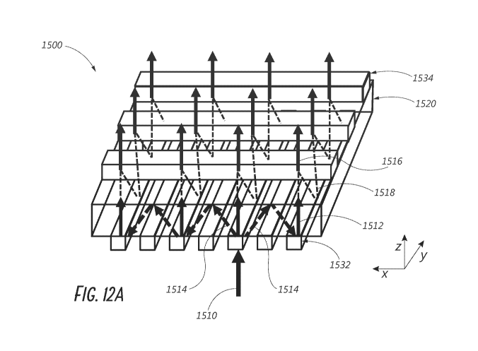
[0028] Figure 12A shows a schematic diagram of light being incoupled,
distributed in two dimensions, and outcoupled by a two-dimensional waveguide
light
multiplexer according to some embodiments.
-5-
CA 03044241 2019-05-16
WO 2018/094093 PCT/US2017/062080
[0029] Figure 12B shows a schematic diagram of light being incoupled,
distributed in two dimensions, and outcoupled by a two-dimensional -waveguide
light
multiplexer according to some other embodiments.
[0030] Figure 13A shows a schematic diagram of light being incoupled
into an
example waveguide, distributed along one direction in one dimension, and
outcoupled via an
example diffraction grating having a preferred diffraction direction.
[0031] Figure 13B shows a schematic diagram of light being incoupled
into an
example waveguide, distributed along two directions in one dimension, and
outcoupled via
two example diffraction gratings having anti-parallel preferred diffraction
directions.
[0032] Figure 13C shows a schematic diagram of light being incoupled
into an
example waveguide at a first location by an example diffraction grating having
a preferred
diffraction direction, and being outcoupled from one side by a second example
diffraction
grating having a preferred diffraction direction at a. second location on the
same side of the
waveguide as the first diffraction grating.
[0033] Figure 13D shows a schematic diagram of light being incoupled
into an
example waveguide at a first location by an example diffraction grating having
a preferred
diffraction direction, and being outcoupled from one side by a second example
diffraction
grating having a preferred diffraction direction at a second location on the
opposite side of
the waveguide as the first diffraction grating.
[0034] Figure 14A shows a schematic diagram of light being incoupled,
distributed in two dimensions, and outcoupled by a two-dimensional waveguide
light
multiplexer comprising crossed asymmetric gratings according to some
embodiments.
[0035] Figure 14B shows a schematic diagram of light being incoupled,
distributed in two dimensions, and outcoupled by a two-dimensional waveguide
light
multiplexer comprising crossed asymmetric gratings according to some other
embodiments.
[0036] Figure 15A shows a schematic diagram of left-handed circularly
polarized
light being incoupled into an example waveguide, distributed along one
direction in one
dimension, and outcoupled via an example polarization grating.
[0037] Figure 15B shows a schematic diagram of right-handed circularly
polarized being transmitted through an example waveguide and polarization
grating.
-6-
CA 03044241 2019-05-16
WO 2018/094093 PCT/US2017/062080
[0038] Figure 15C shows a schematic diagram of light being incoupled
into an
example waveguide, distributed along two directions in one dimension, and
outcoupled via
two example anti-parallel polarization gratings.
[0039] Figure 16A shows a schematic diagram of an example liquid crystal
diffraction grating deposited on an alignment layer overlaying a substrate
according to some
embodiments.
[0040] Figure 16S is a schematic diagram showing a process for forming a
liquid
crystal diffraction grating using a nano-imprint alignment process according
to some
embodiments.
[0041] Figure 16C is a schematic diagram showing a process for forming
liquid
crystal diffraction grating layers having different grating periods using a
nano-imprint
alignment process according to some embodiments.
[0042] Figure 16D shows a schematic diagram of an anti-parallel
diffraction
grating comprising two liquid crystal layers having opposite twist angles.
[0043] Figure 16E shows a schematic diagram of light being incoupled
from
multiple incident angles into an example waveguide and distributed in one
direction in one
dimension by an example liquid crystal polarization grating including multiple
layers of
liquid crystal material having different tilt angles according to some
embodiments.
[0044] Figure 16F shows a schematic diagram of light being incoupled
from
multiple incident angles into an example waveguide and distributed in two
directions in one
dimension by two antiparallel example liquid crystal polarization gratings
including multiple
layers of liquid crystal material having different tilt angles according to
some embodiments.
[0045] Figure 17A shows a schematic diagram of light being incoupled,
distributed in two dimensions, and outcoupled by a two-dimensional waveguide
light
multiplexer comprising crossed polarization gratings according to some
embodiments.
[0046] Figure 17B shows a schematic diagram of light being incoupled,
distributed in two dimensions, and outcoupled by a two-dimensional waveguide
light
multiplexer comprising crossed polarization gratings according to some other
embodiments.
[0047] Figure 17C shows a schematic diagram of light being incoupled,
distributed in two dimensions, and outcoupled by a two-dimensional waveguide
light
-7-
CA 03044241 2019-05-16
WO 2018/094093 PCT/US2017/062080
multiplexer comprising crossed polarization gratings fabricated using a nano-
imprinting
process according to some embodiments.
[0048] Figure 17D shows a schematic diagram of light being incoupled
from
multiple incident angles, distributed in two dimensions, and outcoupled at
multiple angles by
a two-dimensional waveguide light multiplexer comprising crossed polarization
gratings
according to some embodiments.
[0049] The drawings are provided to illustrate example embodiments and
are not
intended to limit the scope of the disclosure.
DETAILED DESCRIPTION
[0050] in some embodiments, optical elements are described herein which
can
distribute light incident upon the optical element in two dimensions via
diffraction. That is, a
ray of light incident upon a surface of the optical element at a location can
propagate through
the optical element in two dimensions, for example along a length and a width
of the optical
element. The incoupled light may also be directed out of the optical element,
or outcoupled
from the optical element, at a plurality of locations that are distributed in
two dimensions on
a surface of the optical element.
[0051] In some embodiments, an optical element as described herein may
be used
as a light distributing element, for example as a light distributing element
that can distribute
light into and/or out of a corresponding waveguide. In some embodiments, an
optical element
as described herein may be used as, for example, an orthogonal pupil expander
(OPE) which
can both deflect or distribute light and can also increase the beam or spot
size of this light as
it propagates. Advantageously, and according to some embodiments, a two-
dimensional
waveguide light multiplexer can serve to efficiently direct and distribute
optical signals in the
form of light to other optical elements in an augmented reality device.
Further, a two-
dimensional waveguide light multiplexer as described herein may be useful for
multiplexing
optical signals for optical fiber communication applications.
[0052] In some embodiments, a two-dimensional .waveguide light
multiplexer
may take the form of a waveguide and at least two diffracting gratings. In
some
embodiments, each diffraction grating may have a grating direction and the
diffraction
gratings may be aligned such that the grating direction of a first diffraction
grating is not
-8-
CA 03044241 2019-05-16
WO 2018/094093 PCT/US2017/062080
1
aligned with a grating direction of a second diffraction grating. In some
embodiments, a
grating direction of a first diffraction grating is perpendicular to a grating
direction of a
second diffraction grating. The diffraction gratings may be disposed on a
major surface (e.g.,
a top major surface) of the waveguide. For example, in some embodiments, the
at least two
diffraction gratings may be disposed on a top major surface of a waveguide. In
some
embodiments, the at least two diffraction gratings may be disposed on a bottom
major
surface of a waveguide. In some embodiments, diffraction gratings may be
disposed on both
a top major surface of a waveguide and on a bottom major surface of a
diffraction grating.
[0053] In some embodiments, two diffraction gratings are arranged such
that a
grating direction of a first diffraction grating is perpendicular to the
grating direction of the
second diffraction grating and this arrangement can advantageously allow for
the two-
dimensional distribution of light. That is, in some embodiments, as incoupled
light
propagates through a waveguide it interacts with the diffraction gratings
disposed on the
waveguide such that the incoupled light is outcoupled at a plurality of
locations which are
distributed in two-dimensions over a major surface of the two-dimensional
waveguide light
multiplexer. As light propagates through the waveguide of the two-dimensional
waveguide
light multiplexer it can interact with a first diffraction grating whereby it
is distributed along
the first diffraction grating's diffraction grating. The distributed light
will also interact with
the second diffraction grating whereby the light distributed along a first
direction is
distributed along the second diffraction grating's grating direction to
thereby achieve
distribution of the light in two dimensions, for example along a length
dimension and along a
width dimension of a two-dimensional waveguide light multiplexer.
[0054] In some embodiments, the diffraction gratings of the two-
dimensional
waveguide light multiplexer may have preferred diffraction directions. In some
embodiments, a diffraction grating may comprise structural features that
provide a preferred
diffraction direction. In some embodiments, a diffraction grating may be, for
example, a
blazed grating, a Bragg grating, a liquid crystal grating, a sinusoidal
grating, a binary grating,
a volume phase grating, or a meta-surface grating. In some embodiments, a
diffraction
grating may be an asymmetric diffraction grating. In some embodiments, a
diffraction grating
may be a polarization grating, for example a liquid crystal polarization
grating. In some
embodiments, where a diffraction grating is a polarization grating the
diffraction grating may
-9-
CA 03044241 2019-05-16
WO 2018/094093 PCT/US2017/062080
comprise liquid crystal material. In some embodiments, the liquid crystal
material may
comprise nematic liquid crystals or cholesteric liquid crystal. In some
embodiments, the
liquid crystal material may comprise azo-containing polymers. In some
embodiments, the
liquid crystal material may comprise polymerizable liquid crystal materials.
In some
embodiments, the liquid crystal material may comprise reactive mesogens.
[0055] In some embodiments, a liquid crystal polarization grating may be
fabricated by a nano-imprinting process. In some embodiments, a liquid crystal
polarization
grating may be fabricated by depositing liquid crystal material on an
alignment layer. In
some embodiments, a liquid crystal polarization grating may not comprise an
alignment
layer.
[0056] In some embodiments, a liquid crystal polarization grating may
comprise
one or more chiral liquid crystal layers, with each layer of the same
chirality having a
different a different tilt angle. By providing multiple liquid crystal layers
having multiple
different tilt angles, the liquid crystal polarization grating can achieve
high diffraction
efficiencies for a broader range of incident angles of light than a liquid
crystal polarization
grating that does not comprise layers having multiple tilt angles. In this
way, a two-
dimensional waveguide light multiplexer comprising perpendicular liquid
crystal polarization
gratings comprising a plurality of liquid crystal layers, each having a
plurality of tilt angles,
can efficiently distribute light at a wide range of incident angles in two
dimensions. Such a
two-dimensional waveguide light multiplexer may be used to, for example,
efficiently
multiplex an image having a wide field-of-view, such as fbr a large pupil or
large eye box,
for an augmented reality device.
[0057] Reference will now be made to the drawings, in which like
reference
numerals refer to like parts throughout.
[0058] Figure 2 illustrates an example of wearable display system 80.
The
display system 80 includes a display 62, and various mechanical and electronic
modules and
systems to support the functioning of that display 62. The display 62 may be
coupled to a
frame 64, which is wearable by a display system user or viewer 60 and which is
configured
to position the display 62 in front of the eyes of the user 60. The display 62
may be
considered eyewear in some embodiments. In some embodiments, a speaker 66 is
coupled to
the frame 64 and positioned adjacent the ear canal of the user 60 (in some
embodiments,
-10-
CA 03044241 2019-05-16
a WO 2018/094093 PCT/US2017/062080
another speaker, not shown, is positioned adjacent the other ear canal of the
user to provide
for stereo/shapeable sound control). In some embodiments, the display system
may also
include one or more microphones 67 or other devices to detect sound. In some
embodiments,
the microphone is configured to allow the user to provide inputs or commands
to the system
80 (e.g., the selection of voice menu commands, natural language questions,
etc.), and/or
may allow audio communication with other persons (e.g., with other users of
similar display
systems). The microphone may further be configured as a peripheral sensor to
continuously
collect audio data (e.g., to passively collect from the user and/or
environment). Such audio
data may include user sounds such as heavy breathing, or environmental sounds,
such as a
loud bang indicative of a nearby event. The display system may also include a
peripheral
sensor 30a, which may be separate from the frame 64 and attached to the body
of the user 60
(e.g., on the head, torso, an extremity, etc. of the user 60). The peripheral
sensor 30a may be
configured to acquire data characterizing the physiological state of the user
60 in some
embodiments, as described further herein. For example, the sensor 30a may be
an electrode.
[0059] With continued reference to Figure 2, the display 62 is
operatively coupled
by communications link 68, such as by a wired lead or wireless connectivity,
to a local data
processing module 70 which may be mounted in a variety of configurations, such
as fixedly
attached to the frame 64, fixedly attached to a helmet or hat worn by the
user, embedded in
headphones, or otherwise removably attached to the user 60 (e.g., in a
backpack-style
configuration, in a belt-coupling style configuration). Similarly, the sensor
30a may be
operatively coupled by communications link 30b, e.g., a wired lead or wireless
connectivity,
to the local processor and data module 70. The local processing and data
module 70 may
comprise a hardware processor, as well as digital memory, such as non-volatile
memory
(e.g., flash memory or hard disk drives), both of which may be utilized to
assist in the
processing, caching, and storage of data. The data include data a) captured
from sensors
(which may be, e.g., operatively coupled to the frame 64 or otherwise attached
to the user
60), such as image capture devices (such as cameras), microphones, inertial
measurement
units, accelerometers, compasses, CPS units, radio devices, gyros, and/or
other sensors
disclosed herein; and/or b) acquired and/or processed using remote processing
module 72
and/or remote data repository 74 (including data relating to virtual content),
possibly for
passage to the display 62 after such processing or retrieval. The local
processing and data
-11-
CA 03044241 2019-05-16
WO 2018/094093 PCT/US2017/062080
module 70 may be operatively coupled by communication links 76, 78, such as
via a wired or
wireless communication links, to the remote processing module 72 and remote
data
repository 74 such that these remote modules 72, 74 are operatively coupled to
each other
and available as resources to the local processing and data module 70. In some
embodiments, the local processing and data module 70 may include one or more
of the image
capture devices, microphones, inertial measurement units, accelerometers,
compasses, GPS
units, radio devices, and/or gyros. In some other embodiments, one or more of
these sensors
may be attached to the frame 64, or may be standalone structures that
communicate with the
local processing and data module 70 by wired or wireless communication
pathways.
100601 With continued reference to Figure 2, in some embodiments, the
remote
processing module 72 may comprise one or more processors configured to analyze
and
process data and/or image information. In some embodiments, the remote data
repository 74
may comprise a digital data storage facility, which may be available through
the internet or
other networking configuration in a "cloud" resource configuration. In some
embodiments,
the remote data repository 74 may include one or more remote servers, which
provide
information, e.g., information for generating augmented reality content, to
the local
processing and data module 70 and/or the remote processing module 72. In some
embodiments, all data is stored and all computations are performed in the
local processing
and data module, allowing fully autonomous use from a remote module.
[00611 The perception of an image as being "three-dimensional" or "3-D"
may be
achieved by providing slightly different presentations of the image to each
eye of the viewer.
Figure 3 illustrates a conventional display system for simulating three-
dimensional imagery
for a user. Two distinct images 5, 7¨one for each eye 4, 6¨are outputted to
the user. The
images 5, 7 are spaced from the eyes 4, 6 by a distance 10 along an optical or
z-axis parallel
to the line of sight of the viewer. The images 5, 7 are flat and the eyes 4, 6
may focus on the
images by assuming a single accommodated state. Such systems rely on the human
visual
system to combine the images 5, 7 to provide a perception of depth and/or
scale for the
combined image.
100621 It will be appreciated, however, that the human visual system is
more
complicated and providing a realistic perception of depth is more challenging.
For example,
many viewers of conventional "3-D" display systems find such systems to be
uncomfortable
-12-
=
CA 03044241 2019-05-16
WO 2018/094093 PCT/US2017/062080
or may not perceive a sense of depth at all. Without being limited by theory,
it is believed
that viewers of an object may perceive the object as being "three-dimensional"
due to a
combination of vergence and accommodation. Vergence movements (i.e., rotation
of the
eyes so that the pupils move toward or away from each other to converge the
lines of sight of
the eyes to fixate upon an object) of the two eyes relative to each other are
closely associated
with focusing (or "accommodation") of the lenses and pupils of the eyes. Under
normal
conditions, changing the focus of the lenses of the eyes, or accommodating the
eyes, to
change focus from one object to another object at a different distance will
automatically
cause a matching change in vergence to the same distance, under a relationship
known as the
"accommodation-vergence reflex," as well as pupil dilation or constriction.
Likewise, a
change in vergence will trigger a matching change in accommodation of lens
shape and pupil
size, under normal conditions. As noted herein, many stereoscopic or "3-D"
display systems
display a scene using slightly different presentations (and, so, slightly
different images) to
each eye such that a three-dimensional perspective is perceived by the human
visual system.
Such systems are uncomfortable for many viewers, however, since they, among
other things,
simply provide a different presentation of a scene, but with the eyes viewing
all the image
information at a single accommodated state, and work against the
"accommodation-vergence
reflex." Display systems that provide a better match between accommodation and
vergence
may form more realistic and comfortable simulations of three-dimensional
imageiy
contributing to increased duration of wear and in turn compliance to
diagnostic and therapy
protocols.
[0063] Figure 4 illustrates aspects of an approach for simulating three-
dimensional imagery using multiple depth planes. With reference to Figure 4,
objects at
various distances from eyes 4, 6 on the z-axis are accommodated by the eyes 4,
6 so that
those objects are in focus. The eyes (4 and 6) assume particular accommodated
states to
bring into focus objects at different distances along the z-axis.
Consequently, a particular
accommodated state may be said to be associated with a particular one of depth
planes 14,
with has an associated focal distance, such that objects or parts of objects
in a particular
depth plane are in focus when the eye is in the accommodated state for that
depth plane. In
some embodiments, three-dimensional imagery may be simulated by providing
different
presentations of an image for each of the eyes 4, 6, and also by providing
different
-13-
CA 03044241 2019-05-16
WO 2018/094093 PCT/US2017/062080
presentations of the image corresponding to each of the depth planes. While
shown as being
separate for clarity of illustration, it will be appreciated that the fields
of view of the eyes 4, 6
may overlap, for example, as distance along the z-axis increases. In addition,
while shown as
flat for ease of illustration, it will be appreciated that the contours of a
depth plane may be
curved in physical space, such that all features in a depth plane are in focus
with the eye in a
particular accommodated state.
[0064] The distance between an object and the eye 4 or 6 may also change
the
amount of divergence of light from that object, as viewed by that eye. Figures
5A-5C
illustrates relationships between distance and the divergence of light rays.
The distance
between the object and the eye 4 is represented by, in order of decreasing
distance, R1, R2,
and R3. As shown in Figures 5A-5C, the light rays become more divergent as
distance to the
object decreases. As distance increases, the light rays become more
collimated. Stated
another way, it may be said that the light field produced by a point (the
object or a part of the
object) has a spherical wavefront curvature, which is a function of how far
away the point is
from the eye of the user. The curvature increases with decreasing distance
between the
object and the eye 4. Consequently, at different depth planes, the degree of
divergence of
light rays is also different, with the degree of divergence increasing with
decreasing distance
between depth planes and the viewer's eye 4. While only a single eye 4 is
illustrated for
clarity of illustration in Figures 5A-5C and other figures herein, it will be
appreciated that the
discussions regarding eye 4 may be applied to both eyes 4 and 6 of a viewer.
[0065] Without being limited by theory, it is believed that the human
eye
typically can interpret a finite number of depth planes to provide depth
perception.
Consequently, a highly believable simulation of perceived depth may be
achieved by
providing, to the eye, different presentations of an image corresponding to
each of these
limited number of depth planes. The different presentations may be separately
focused by
the viewer's eyes, thereby helping to provide the user with depth cues based
on the
accommodation of the eye required to bring into focus different image features
for the scene
located on different depth plane and/or based on observing different image
features on
different depth planes being out of focus.
[0066] Figure 6 illustrates an example of a waveguide stack for
outputting image
information to a user. A display system 1000 includes a stack of waveguides,
or stacked
-14-
CA 03044241 2019-05-16
WO 2018/094093 PCT/1JS2017/062080
waveguide assembly, 178 that may be utilized to provide three-dimensional
perception to the
eye/brain using a plurality of waveguides 182, 184, 186, 188, 190. In some
embodiments,
the display system 1000 is the system 80 of Figure 2, with Figure 6
schematically showing
some parts of that system 80 in greater detail. For example, the waveguide
assembly 178
may be part of the display 62 of Figure 2. It will be appreciated that the
display system 1000
may be considered a light field display in some embodiments.
[0067] With continued reference to Figure 6, the waveguide assembly 178
may
also include a plurality of features 198, 196, 194, 192 between the
waveguides. In some
embodiments, the features 198, 196, 194, 192 may be one or more lenses. The
waveguides
182, 184, 186, 188, 190 and/or the plurality of lenses 198, 196, 194, 192 may
be configured
to send image information to the eye with various levels of wavefront
curvature or light ray
divergence. Each waveguide level may be associated with a particular depth
plane and may
be configured to output image information corresponding to that depth plane.
Image
injection devices 200, 202, 204, 206, 208 may function as a source of light
for the
waveguides and may be utilized to inject image information into the waveguides
182, 184,
186, 188, 190, each of which may be configured, as described herein, to
distribute incoming
light across each respective waveguide, for output toward the eye 4. Light
exits an output
surface 300, 302, 304, 306, 308 of the image injection devices 200, 202, 204,
206, 208 and is
injected into a corresponding input surface 382, 384, 386, 388, 390 of the
waveguides 182,
184, I 86, l 88, 190. In some embodiments, the each of the input surfaces 382,
384, 386, 388,
390 may be an edge of a corresponding waveguide, or may be part of a major
surface of the
corresponding waveguide (that is, one of the waveguide surfaces directly
facing the world
144 or the viewer's eye 4). In some embodiments, a single beam of light (e.g.
a collimated
beam) may be injected into each waveguide to output an entire field of cloned
collimated
beams that are directed toward the eye 4 at particular angles (and amounts of
divergence)
corresponding to the depth plane associated with a particular waveguide. In
some
embodiments, a single one of the image injection devices 200, 202, 204, 206,
208 may be
associated with and inject light into a plurality (e.g., three) of the
waveguides 182, 184, 186,
188, 190.
[0068] In some embodiments, the image injection devices 200, 202, 204,
206, 208
are discrete displays that each produce image information for injection into a
corresponding
-15-
CA 03044241 2019-05-16
WO 2018/094093 PCT/US2017/062080
waveguide 182, 184, 186, 188, 190, respectively. In some other embodiments,
the image
injection devices 200, 202, 204, 206, 208 are the output ends of a single
multiplexed display
which may, e.g., pipe image information via one or more optical conduits (such
as fiber optic
cables) to each of the image injection devices 200, 202, 204, 206, 208. It
will be appreciated
that the image information provided by the image injection devices 200, 202,
204, 206, 208
may include light of different wavelengths, or colors (e.g., different
component colors, as
discussed herein).
100691 In some embodiments, the light injected into the waveguides 182,
184,
186, 188, 190 is provided by a light projector system 2000, which comprises a
light module
2040, which may include a light emitter, such as a light emitting diode (LED).
The light
from the light module 2040 may be directed to and modified by a light
modulator 2030, e.g.,
a spatial light modulator, via a beam splitter 2050. The light modulator 2030
may be
configured to change the perceived intensity of the light injected into the
waveguides 182,
184, 186, 188, 190. Examples of spatial light modulators include liquid
crystal displays
(LCD) including a liquid crystal on silicon (LCOS) displays.
[00701 In some embodiments, the display system 1000 may be a scanning
fiber
display comprising one or more scanning fibers configured to project light in
various patterns
(e.g., raster scan, spiral scan, Lissajous patterns, etc.) into one or more
waveguides 182, 184,
186, 188, 190 and ultimately to the eye 4 of the viewer. In some embodiments,
the illustrated
image injection devices 200, 202, 204, 206, 208 may schematically represent a
single
scanning fiber or a bundles of scanning fibers configured to inject light into
one or a plurality
of the waveguides 182, 184, 186, 188, 190. In some other embodiments, the
illustrated
image injection devices 200, 202, 204, 206, 208 may schematically represent a
plurality of
scanning fibers or a plurality of bundles of scanning, fibers each of which
are configured to
inject light into an associated one of the waveguides 182, 184, 186, 188, 190.
It will be
appreciated that the one or more optical fibers may be configured to transmit
light from the
light module 2040 to the one or more waveguides 182, 184, 186, 188, 190. It
will be
appreciated that one or more intervening optical structures may be provided
between the
scanning fiber, or fibers, and the one or more waveguides 182, 184, 186, 188,
190 to, e.g.,
redirect light exiting the scanning fiber into the one or more waveguides 182,
184, 186, 188,
190.
-16-
CA 03044241 2019-05-16
WO 2018/094093 PCT/US2017/062080
[0071] A controller 210 controls the operation of one or more of the
stacked
waveguide assembly 178, including operation of the image injection devices
200, 202, 204,
206, 208, the light source 2040, and the light modulator 2030. In some
embodiments, the
controller 210 is part of the local data processing module 70. The controller
210 includes
programming (e.g., instructions in a non-transitory medium) that regulates the
timing and
provision of image information to the waveguides 182, 184, 186, 188, 190
according to, e.g.,
any of the various schemes disclosed herein. In some embodiments, the
controller may be a
single integral device, or a distributed system connected by wired or wireless
communication
channels. The controller 210 may be part of the processing modules 70 or 72
(Figure 1) in
some embodiments.
[0072] With continued reference to Figure 6, the waveguides 182, 184,
186, 188,
190 may be configured to propagate light within each respective waveguide by
total internal
reflection (T1R). The waveguides 182, 184, 186, 188, 190 may each be planar or
have
another shape (e.g., curved), with major top and bottom. surfaces and edges
extending
between those major top and bottom surfaces. In the illustrated configuration,
the
waveguides 182, 184, 186, 188, 190 may each include outcoupling optical
elements 282,
284, 286, 288, 290 that are configured to extract light out of a waveguide by
redirecting the
light, propagating within each respective waveguide, out of the waveguide to
output image
information to the eye 4. Extracted light may also be referred to as
outcoupled light and the
outcoupling optical elements light may also be referred to light extracting
optical elements.
An extracted beam of light is outputted by the waveguide at locations at which
the light
propagating in the waveguide strikes a light extracting optical element. The
outcoupling
optical elements 282, 284, 286, 288, 290 may, for example, be gratings,
including diffractive
optical features, as discussed further herein. While illustrated disposed at
the bottom major
surfaces of the waveguides 182, 184, 186, 188, 190 for ease of description and
drawing
clarity, in some embodiments, the outcoupling optical elements 282, 284, 286,
288, 290 may
be disposed at the top and/or bottom major surfaces, and/or may be disposed
directly in the
volume of the waveguides 182, 184, 186, 188, 190, as discussed further herein.
In some
embodiments, the outcoupling optical elements 282, 284, 286, 288, 290 may be
formed in a
layer of material that is attached to a transparent substrate to form the
waveguides 182, 184,
186, 188, 190. In some other embodiments, the waveguides 182, 184, 186, 188,
190 may be
-17-
CA 03044241 2019-05-16
WO 2018/094093 PCT/US2017/062080
a monolithic piece of material and the outcoupling optical elements 282, 284,
286, 288, 290
may be formed on a surface and/or in the interior of that piece of material.
[0073] With continued reference to Figure 6, as discussed herein, each
waveguide
182, 184, 186, 188, 190 is configured to output light to form an image
corresponding to a
particular depth plane. For example, the waveguide 182 nearest the eye may be
configured
to deliver collimated light, as injected into such waveguide 182, to the eye
4. The collimated
light may be representative of the optical infinity focal plane. The next
waveguide up 184
may be configured to send out collimated light which passes through the first
lens 192 (e.g., a
negative lens) before it can reach the eye 4; such first lens 192 may be
configured to create a
slight convex wavefront curvature so that the eye/brain interprets light
coming from that next
waveguide up 184 as coming from a first focal plane closer inward toward the
eye 4 from
optical infinity. Similarly, the third up waveguide 186 passes its output
light through both
the first 192 and second 194 lenses before reaching the eye 4; the combined
optical power of
the first 192 and second 194 lenses may be configured to create another
incremental amount
of wavefront curvature so that the eye/brain interprets light coming from the
third waveguide
186 as coming from a second focal plane that is even closer inward toward the
person from
optical infinity than was light from the next waveguide up 184.
[0074] The other waveguide layers 188, 190 and lenses 196, 198 are
similarly
configured, with the highest waveguide 190 in the stack sending its output
through all of the
lenses between it and the eye for an aggregate focal power representative of
the closest focal
plane to the person. To compensate for the stack of lenses 198, 196, 194, 192
when
viewing/interpreting light coming from the world 144 on the other side of the
stacked
waveguide assembly 178, a compensating lens layer 180 may be disposed at the
top of the
stack to compensate for the aggregate power of the lens stack 198, 196, 194,
192 below.
Such a configuration provides as many perceived focal planes as there are
available
waveguide/lens pairings. Both the outcoupling optical elements of the
waveguides and the
focusing aspects of the lenses may be static (i.e., not dynamic or electro-
active). In some
alternative embodiments, either or both may be dynamic using electro-active
features.
100751 In some embodiments, two or more of the waveguides 182, 184, 186,
188,
190 may have the same associated depth plane. For example, multiple waveguides
182, 184,
186, 188, 190 may be configured to output images set to the same depth plane,
or multiple
-18-
CA 03044241 2019-05-16
WO 2018/094093 PCT/US2017/062080
=
subsets of the waveguides 182, 184, 186, 188, 190 may be configured to output
images set to
the same plurality of depth planes, with one set for each depth plane. This
can provide
advantages for forming a tiled image to provide an expanded field of view at
those depth
planes.
[0076] With continued reference to Figure 6, the outcoupling optical
elements
282, 284, 286, 288, 290 may be configured to both redirect light out of their
respective
waveguides and to output this light with the appropriate amount of divergence
or collimation
for a particular depth plane associated with the waveguide. As a result,
waveguides having
different associated depth planes may have different configurations of
outcoupling optical
elements 282, 284, 286, 288, 290, which output light with a different amount
of divergence
depending on the associated depth plane. In some embodiments, the light
extracting optical
elements 282, 284, 286, 288, 290 may be volumetric or surface features, which
may be
configured to output light at specific angles. For example, the light
extracting optical
elements 282, 284, 286, 288, 290 may be volume holograms, surface holograms,
and/or
diffraction gratings. In some embodiments, the features 198, 196, 194, 192 may
not be
lenses; rather, they may simply be spacers (e.g., cladding layers and/or
structures for forming
air gaps).
[0077] In some embodiments, the outcoupling optical elements 282, 284,
286,
288, 290 are diffractive features that form a diffraction pattern, or
"diffractive optical
element" (also referred to herein as a "DOE"). Preferably, the D()E's have a
sufficiently low
diffraction efficiency so that only a portion of the light of the beam is
deflected away toward
the eye 4 with each intersection of the DOE, while the rest continues to move
through a
waveguide via total internal reflection. The light carrying the image
information is thus
divided into a number of related exit beams that exit the waveguide at a
multiplicity of
locations and the result is a fairly uniform pattern of exit emission toward
the eye 4 for this
particular collimated beam bouncing around within a waveguide.
[0078] In some embodiments, one or more DOEs may be switchable between
"on" states in which they actively diffract, and "off' states in which they do
not significantly
diffract. For instance, a switchable DOE may comprise a layer of polymer
dispersed liquid
crystal, in which microdroplets comprise a diffraction pattern in a host
medium, and the
refractive index of the microdroplets may be switched to substantially match
the refractive
-19-
CA 03044241 2019-05-16
WO 2018/094093 PCT/US2017/062080
index of the host material (in which case the pattern does not appreciably
diffract incident
light) or the microdroplet may be switched to an index that does not match
that of the host
medium (in which case the pattern actively diffracts incident light).
100791 In some embodiments, a camera assembly 500 (e.g., a digital
camera,
including visible light and infrared light cameras) may be provided to capture
images of the
eye 4 and/or tissue around the eye 4 to, e.g., detect user inputs and/or to
monitor the
physiological state of the user. As used herein, a camera may be any image
capture device.
In some embodiments, the camera assembly 500 may include an image capture
device and a
light source to project light (e.g., infrared light) to the eye, which may
then be reflected by
the eye and detected by the image capture device. In some embodiments, the
camera
assembly 500 may be attached to the frame 64 (Figure 2) and may be in
electrical
communication with the processing modules 70 and/or 72, which may process
image
information from the camera assembly 500 to make various determinations
regarding, e.g.,
the physiological state of the user, as discussed herein. It will be
appreciated that
information regarding the physiological state of user may be used to determine
the behavioral
or emotional state of the user. Examples of such information include movements
of the user
and/or facial expressions of the user. The behavioral or emotional state of
the user may then
be triangulated with collected environmental and/or virtual content data. so
as to determine
relationships between the behavioral or emotional state, physiological state,
and
environmental or virtual content data. In some embodiments, one camera
assembly 500 may
be utilized for each eye, to separately monitor each eye.
[0080] With reference now to Figure 7, an example of exit beams
outputted by a
waveguide is shown. One waveguide is illustrated, but it will be appreciated
that other
waveguides in the waveguide assembly 178 (Figure 6) may function similarly,
where the
waveguide assembly 178 includes multiple waveguides. Light 400 is injected
into the
waveguide 182 at the input surface 382 of the waveguide 182 and propagates
within the
waveguide 182 by Tilt. At points where the light 400 impinges on the DOE 282,
a portion of
the light exits the waveguide as exit beams 402. The exit beams 402 are
illustrated as
substantially parallel but, as discussed herein, they may also be redirected
to propagate to the
eye 4 at an angle (e.g., forming divergent exit beams), depending on the depth
plane
associated with the waveguide 182. It will be appreciated that substantially
parallel exit
-20-
CA 03044241 2019-05-16
WO 2018/094093 PCT/US2017/062080
beams may be indicative of a waveguide with outcoupling optical elements that
outcouple
light to form images that appear to be set on a depth plane at a large
distance (e.g., optical
infinity) from the eye 4. Other waveguides or other sets of outcoupling
optical elements may
output an exit beam pattern that is more divergent, which would require the
eye 4 to
accommodate to a closer distance to bring it into focus on the retina and
would be interpreted
by the brain as light from a distance closer to the eye 4 than optical
infinity.
[0081] In some embodiments, a full color image may be formed at each
depth
plane by overlaying images in each of the component colors, e.g., three or
more component
colors. Figure 8 illustrates an example of a stacked waveguide assembly in
which each depth
plane includes images formed using multiple different component colors. The
illustrated
embodiment shows depth planes 14a ¨ 14f, although more or fewer depths are
also
contemplated. Each depth plane may have three component color images
associated with it:
a first image of a first color, G; a second image of a second color, R; and a
third image of a
third color, B. Different depth planes are indicated in the figure by
different numbers for
diopters (dpt) following the letters G, R, and B. Just as examples, the
numbers following
each of these letters indicate diopters (1/m), or inverse distance of the
depth plane from a
viewer, and each box in the figures represents an individual component color
image. In some
embodiments, to account for differences in the eye's focusing of light of
different
wavelengths, the exact placement of the depth planes for different component
colors may
vary. For example, different component color images for a given depth plane
may be placed
on depth planes corresponding to different distances from the user. Such an
arrangement
may increase visual acuity and user comfort and/or may decrease chromatic
aberrations.
[0082] In some embodiments, light of each component color may be
outputted by
a single dedicated waveguide and, consequently, each depth plane may have
multiple
waveguides associated with it In such embodiments, each box in the figures
including the
letters G, R, or B may be understood to represent an individual waveguide, and
three
waveguides may be provided per depth plane where three component color images
are
provided per depth plane. While the waveguides associated with each depth
plane are shown
adjacent to one another in this drawing for ease of description, it will be
appreciated that, in a
physical device, the waveguides may all be arranged in a stack with one
waveguide per level.
-21-
CA 03044241 2019-05-16
WO 2018/094093 PCT/US2017/062080
=
In some other embodiments, multiple component colors may be outputted by the
same
waveguide, such that, e.g., only a single waveguide may be provided per depth
plane.
[0083] With
continued reference to Figure 8, in some embodiments, G is the color
green, R is the color red, and B is the color blue. In some other embodiments,
other colors
associated with other wavelengths of light, including magenta and cyan, may be
used in
addition to or may replace one or more of red, green, or blue. In some
embodiments, features
198, 196, 194, and 192 may be active or passive optical filters configured to
block or
selectively light from the ambient environment to the viewer's eyes.
[0084] It will be
appreciated that references to a given color of light throughout
this disclosure will be understood to encompass light of one or more
wavelengths within a
range of wavelengths of light that are perceived by a viewer as being of that
given color. For
example, red light may include light of one or more wavelengths in the range
of about 620-
780 nm, green light may include light of one or more wavelengths in the range
of about 492-
577 nm, and blue light may include light of one or more wavelengths in the
range of about
435-493 nm.
[0085] In some
embodiments, the light source 2040 (Figure 6) may be configured
to emit light of one or more wavelengths outside the visual perception range
of the viewer,
for example, infrared and/or ultraviolet wavelengths. In
addition, the incoupling,
outcoupling, and other light redirecting structures of the waveguides of the
display 1000 may
be configured to direct and emit this light out of the display towards the
user's eye 4, e.g., for
imaging andlor user stimulation applications.
[0086] With
reference now to Figure 9A, in some embodiments, light impinging
on a waveguide may need to be redirected to incouple that light into the
waveguide. An
incoupling optical element may be used to redirect and incouple the light into
its
corresponding waveguide. Figure 9A illustrates a cross-sectional side view of
an example of
a plurality or set 1200 of stacked waveguides that each includes an incoupling
optical
element. The waveguides may each be configured to output light of one or more
different
wavelengths, or one or more different ranges of wavelengths. It will be
appreciated that the
stack 1200 may correspond to the stack 178 (Figure 61) and the illustrated
waveguides of the
stack 1200 may correspond to part of the plurality of waveguides 182, 184,
186, 188, 190,
except that light from one or more of the image injection devices 200, 202,
204, 206, 208 is
-22-
CA 03044241 2019-05-16
WO 2018/094093 PCT/US2017/062080
injected into the waveguides from a position that requires light to be
redirected for
incoupling.
[0087] The illustrated set 1200 of stacked waveguides includes
waveguides 1210,
1220, and 1230. Each waveguide includes an associated incoupling optical
element (which
may also be referred to as a light input area on the waveguide), with, e.g.,
incoupling optical
element 1212 disposed on a major surface (e.g., an upper major surface) of
waveguide 1210,
incoupling optical element 1224 disposed on a major surface (e.g., an upper
major surface) of
waveguide 1220, and incoupling optical element 1232 disposed on a major
surface (e.g., an
upper major surface) of waveguide 1230. In some embodiments, one or more of
the
incoupling optical elements 1212, 1222, 1232 may be disposed on the bottom
major surface
of the respective waveguide 1210, 1220, 1230 (particularly where the one or
more incoupling
optical elements are reflective, deflecting optical elements). As illustrated,
the incoupling
optical elements 1212, 1222, 1232 may be disposed on the upper major surface
of their
respective waveguide 1210, 1220, 1230 (or the top of the next lower
waveguide), particularly
where those incoupling optical elements are transmissive, deflecting optical
elements, In
some embodiments, the incoupling optical elements 1212, 1222, 1232 may be
disposed in the
body of the respective waveguide 1210, 1220, 1230. In some embodiments, as
discussed
herein, the incoupling optical elements 1212, 1222, 1232 are wavelength
selective, such that
they selectively redirect one or more wavelengths of light, while transmitting
other
wavelengths of light. While illustrated on one side or corner of their
respective waveguide
1210, 1220, 1230, it will be appreciated that the incoupling optical elements
1212, 1222,
1232 may be disposed in other areas of their respective waveguide 1210, 1220,
1230 in sonic
embodiments.
[0088] As illustrated, the incoupling optical elements 1212, 1222, 1232
may be
laterally offset from one another. In some embodiments, each incoupling
optical element
may be offset such that it receives light without that light passing through
another incoupling
optical element. For example, each incoupling optical element 1212, 1222, 1232
may be
configured to receive light from a different image injection device 200, 202,
204, 206, and
208 as shown in Figure 6, and may be separated (e.g., laterally spaced apart)
from other
incoupling optical elements 1212, 1222, 1232 such that it substantially does
not receive light
from the other ones of the incoupling optical elements 1212, 1222, 1232.
-23-
CA 03044241 2019-05-16
WO 2018/094093 PCT/US2017/062080
[0089] Each waveguide also includes associated light distributing
elements, with,
e.g., light distributing elements 1214 disposed on a major surface (e.g., a
top major surface)
of waveguide 1210, light distributing elements 1224 disposed on a major
surface (e.g., a top
major surface) of waveguide 1220, and light distributing elements 1234
disposed on a major
surface (e.g., a top major surface) of waveguide 1230. In some other
embodiments, the light
distributing elements 1214, 1224, 1234, may be disposed on a bottom major
surface of
associated waveguides 1210, 1220, 1230, respectively. In some other
embodiments, the light
distributing elements 1214, 1224, 1234, may be disposed on both top and bottom
major
surface of associated waveguides 1210, 1220, 1230, respectively; or the light
distributing
elements 1214, 1224, 1234, may be disposed on different ones of the top and
bottom major
surfaces in different associated waveguides 1210, 1220, 1230, respectively.
[0090] The waveguides 1210, 1220, 1230 may be spaced apart and separated
by,
e.g., gas, liquid, and/or solid layers of material. For example, as
illustrated, layer 1218a may
separate waveguides 1210 and 1220; and layer 1.218b may separate waveguides
1220 and
1230. In some embodiments, the layers 1218a and 1218b are formed of low
refractive index
materials (that is, materials having a lower refractive index than the
material forming the
immediately adjacent one of waveguides 1210, 1220, 1230). Preferably, the
refractive index
of the material forming the layers 1218a, 1218b is 0.05 or more, or 0.10 or
more less than the
refractive index of the material forming the waveguides 1210, 1220, 1230.
Advantageously,
the lower refractive index layers 1218a, 1218b may function as cladding layers
that facilitate
total internal reflection (TIR) of light through the waveguides 1210, 1220,
1230 (e.g., '11R.
between the top and bottom major surfaces of each waveguide). In some
embodiments, the
layers 1218a, 1.21.8b are formed of air. While not illustrated, it will be
appreciated that the
top and bottom of the illustrated set 1200 of waveguides may include
immediately
neighboring cladding layers.
[0091] Preferably, for ease of manufacturing and other considerations,
the
material forming the waveguides 1210, 1220, 1230 are similar or the same, and
the material
forming the layers 1218a, 1218b are similar or the same. In some embodiments,
the material
forming the waveguides 1210, 1220, 1230 may be different between one or more
waveguides, and/or the material forming the layers 1218a, 1218b may be
different, while still
holding to the various refractive index relationships noted above.
-24-
CA 03044241 2019-05-16
WO 2018/094093 PCT/US2017/062080
[0092] With continued reference to Figure 9A, light rays 1240, 1242,
1244 are
incident on the set 1200 of waveguides. It will be appreciated that the light
rays 1240, 1242,
1244 may be injected into the waveguides 1210, 1220, 1230 by one or more image
injection
devices 200, 202, 204, 206, 208 (Figure 6).
[0093] In some embodiments, the light rays 1240, 1242, 1244 have
different
properties, e.g., different wavelengths or different ranges of wavelengths,
which may
correspond to different colors. The incoupling optical elements 1212, 122,
1232 each deflect
the incident light such that the light propagates through a respective one of
the waveguides
1210, 1220, 1230 by TIR.
[0094] For example, incoupling optical element 1212 may be configured to
deflect ray 1240, which has a first wavelength or range of wavelengths,
Similarly, the
transmitted ray 1242 impinges on and is deflected by the incoupling optical
element 1222,
which is configured to deflect light of a second wavelength or range of
wavelengths.
Likewise, the ray 1244 is deflected by the incoupling optical element 1232,
which is
configured to selectively deflect light of third wavelength or range of
wavelengths.
[0095] With continued reference to Figure 9A, the deflected light rays
1240,
1242, 1244 are deflected so that they propagate through a corresponding
waveguide 1210,
1220, 1230; that is, the incoupling optical elements 1212, 1222, 1232 of each
waveguide
deflects light into that corresponding waveguide 1210, 1220, 1230 to incouple
light into that
corresponding waveguide. The light rays 1240, 1242, 1244 are deflected at
angles that cause
the light to propagate through the respective waveguide 1210, 1220, 1230 by
TIR. The light
rays 1240, 1242, 1244 propagate through the respective waveguide 1210, 1220,
1230 by TIR
until impinging on the waveguide's corresponding light distributing elements
1214, 1224,
1234.
100961 With reference now to Figure 9B, a perspective view of an example
of the
plurality of stacked waveguides of Figure 9A is illustrated. As noted above,
the incoupled
light rays 1240, 1242, 1244, are deflected by the incoupling optical elements
1212, 1222,
1232, respectively, and then propagate by TIR within the waveguides 1210,
1220, 1230,
respectively. The light rays 1240, 1242, 1244 then impinge on the light
distributing elements
1214, 1224, 1234, respectively. The light distributing elements 1214, 1224,
1234 deflect the
-25-
CA 03044241 2019-05-16
WO 2018/094093 PCT/US2017/062080
light rays 1240, 1242, 1244 so that they propagate towards the outcoupling
optical elements
1250, 1252, 1254, respectively.
[0097] In some embodiments, the light distributing elements 1214, 1224,
1234
are orthogonal pupil expanders (OPE's). In some embodiments, the OPE's both
deflect or
distribute light to the outcoupling optical elements 1250, 1252, 1254 and also
increase the
beam or spot size of this light as it propagates to the outcoupling optical
elements. In some
embodiments, e.g., where the beam size is already of a desired size, the light
distributing
elements 1214, 1224, 1234 may be omitted and the incoupling optical elements
1212, 1222,
1232 may be configured to deflect light directly to the outcoupling optical
elements 1250,
1252, 1254. For example, with reference to Figure 9A, the light distributing
elements 1214,
1224, 1234 may be replaced with outcoupling optical elements 1250, 1252, 1254,
respectively. In some embodiments, the outcoupling optical elements 1250,
1252, 1254 are
exit pupils (EP's) or exit pupil expanders (EPE's) that direct light in a
viewer's eye 4 (Figure
7).
[0098] Accordingly, with reference to Figures 9A and 9B, in some
embodiments,
the set 1200 of waveguides includes waveguides 1210, 1220, 1230; incoupling
optical
elements 1212, 1222, 1232; light distributing elements (e.g., OPE's) 1214,
1224, 1234; and
outcoupling optical elements (e.g., EP's) 1250, 1252, 1254 for each component
color. The
waveguides 1210, 1220, 1230 may be stacked with an air gap/cladding layer
between each
one. The incoupling optical elements 1212, 1222, 1232 redirect or deflect
incident light
(with different incoupling optical elements receiving light of different
wavelengths) into its
waveguide. The light then propagates at an angle which will result in FIR
within the
respective waveguide 1210, 1220, 1230. In the example shown, light ray 1240
(e.g., blue
light) is deflected by the first incoupling optical element 1212, and then
continues to bounce
down the waveguide, interacting with the light distributing element (e.g.,
OPE's) 1214 and
then the outcoupling optical element (e.g., El's) 1250, in a manner described
earlier. The
light rays 1242 and 1244 (e.g., green and red light, respectively) will pass
through the
waveguide 1210, with light ray 1242 impinging on and being deflected by
incoupling optical
element 1222. The light ray 1242 then bounces down the waveguide 1220 via
Triz,
proceeding on to its light distributing element (e.g., OPEs) 1224 and then the
outcoupling
optical element (e.g., EP's) 1252. Finally, light ray 1244 (e.g., red light)
passes through the
-26-
CA 03044241 2019-05-16
WO 2018/094093 PCT/US2017/062080
waveguide 1220 to impinge on the light incoupling optical elements 1232 of the
waveguide
1230. The light incoupling optical elements 1232 deflect the light ray 1244
such that the
light ray propagates to light distributing element (e.g., OPEs) 1234 by DR,
and then to the
outcoupling optical element (e.g., EPs) 1254 by TIR. The outcoupling optical
element 1254
then finally outcouples the light ray 1244 to the viewer, who also receives
the outcoupled
light from the other waveguides 1210, 1220.
[0099] Figure 9C illustrates a top-down plan view of an example of the
plurality
of stacked waveguides of Figures 9A and 9B. As illustrated, the waveguides
1210, 1220,
1230, along with each waveguide's associated light distributing element 1214,
1224, 1234
and associated outcoupling optical element 1250, 1252, 1254, may be vertically
aligned.
However, as discussed herein, the incoupling optical elements 1212, 1222, 1232
are not
vertically aligned; rather, the incoupling optical elements are preferably non-
overlapping
(e.g., laterally spaced apart as seen in the top-down view). As discussed
further herein, this
nonoverlapping spatial arrangement facilitates the injection of light from
different resources
into different waveguides on a one-to-one basis, thereby allowing a specific
light source to be
uniquely coupled to a specific waveguide. In some embodiments, arrangements
including
nonoverlapping spatially-separated incoupling optical elements may be referred
to as a
shifted pupil system, and the in coupling optical elements within these
arrangements may
correspond to sub pupils.
[0100] Reference will now be made to Figure 10, which shows an example
schematic diagram of incoupled light 1310 propagating through a two-
dimensional
waveguide light multiplexer 1320 according to some embodiments, via TIR. The
light 1310
interacts with the two-dimensional waveguide light multiplexer 1320 as it
propagates and is
distributed, or multiplexed, along two directions in a first dimension, for
example the x-
dimension, whereupon it is outcoupled 1312 in a normal direction from the two-
dimensional
waveguide light multiplexer 1320. The light 1310 also interacts with the two-
dimensional
waveguide light multiplexer 1320 and is multiplexed along two directions in a
second
dimension, for example the y-dimension, whereupon it is outcoupled 1314 from
the two-
dimensional waveguide light multiplexer 1320 in a normal direction. Thus, the
incoupled
light 1310 is multiplexed in two dimensions and outcoupled 1312, 1314 from the
two-
dimensional waveguide light multiplexer 1320.
-27-
CA 03044241 2019-05-16
WO 2018/094093 PCT/US2017/062080
[0101] Figure 11A shows a partial schematic diagram of light 1410 being
incoupled into an example waveguide 1420 by an example diffraction grating
1430 and
propagating via Tilt in some embodiments, the diffraction grating 1430 has a
period (4)
larger than the wavelength of light 1410 (X) divided by the refractive index
(n) of the
waveguide but smaller than the wavelength of light 1410 (X). In some
embodiments, the
diffraction grating 1430 may be a binary or sinusoidal surface relief grating.
In order to
achieve TIR the order diffraction angle (0) is greater than Oc, where 0 and 0c
are such that
n=sin(0) = XJA and n=sin(0c) = 1, in the case where the medium outside of the
waveguide is
air. The incident light 1410 interacts with the diffraction grating 1430 and
is diffracted into
the waveguide 1420, whereupon TIR is achieved. As the diffracted light 1412
propagates
through the waveguide 1420 via TIR, some light encounters and interacts with
the diffraction
grating 1430 multiple times.
[0102] As illustrated in Figure 11B, where the propagating diffracted
light 1412
interacts with the diffraction grating 1430, it is outcoupled from the
waveguide 1420 in two
directions 1414, 1416 along the x-dimension, thereby achieving multiplexing of
the incident
light 1410. This outcoupling occurs via +1 and -1. orders of diffraction.
[0103] Figure 11C demonstrates how the above described phenomenon may be
used to achieve light multiplexing via a first diffraction grating 1432 at a
first location on a
waveguide 1420 and a second diffraction grating 1434 at a second location on
the same
waveguide. Light 1410 is incident upon the first diffraction grating 1432,
whereupon it is
diffracted and propagates via TIR through the waveguide 1420 as described
above. The
propagating light 1412 interacts with a second diffraction grating 1434 at a
second location
on the waveguide 1420, whereupon it is outcoupled in two normal directions
1414, 1416.
Thus a single incident beam or ray of light 1410 incident upon the waveguide
1420 at a first
location may be multiplexed and outcoupled along both directions in the x-
dimension at a
second location.
[0104] In some embodiments, and as shown in Figure 12A, a two-
dimensional
waveguide light multiplexer 1500 can utilize the phenomenon described above
with respect
to Figures 11A-C to achieve the two-dimensional multiplexing of incident light
by including
two diffraction gratings 1532, 1534 disposed over one another. In some
embodiments, a first
-28-
CA 03044241 2019-05-16
WO 2018/094093 PCT/US2017/062080
diffraction grating 1532 is located on a bottom major surface of a waveguide
1520 and a
second diffraction grating 1534 is located on a top major surface of a
waveguide 1520.
[0105] Importantly, each diffraction grating 1532, 1534 has a
corresponding
grating direction and the diffraction gratings 1532, 1534 are arranged such
that the grating
direction of the first diffraction grating 1532 is along the x-dimension and
is perpendicular to
the grating direction of the second diffraction grating 1534, which is along
the y-dimension.
In some embodiments, this arrangement of two diffraction gratings wherein the
grating
direction of a first diffraction grating is perpendicular to the grating
direction of a second
diffraction grating may be referred to as crossed diffraction gratings.
According to some
embodiments, and as shown in Figure 12A, the grating direction corresponds to
the physical
orientation of the diffraction grating 1532, 1534.
[0106] In use, incident light 1510 interacts with the first diffraction
grating 1532
whereby it is diffracted and spread along both directions in the x-dimension.
The diffracted
light propagates through the waveguide 1520 via TIR. As the light propagates
it may interact
with the first diffraction grating 1532 again and be diffracted and sometimes
outcoupled
1512 out of the waveguide 1520. Some of the diffractive light 1512 however
interacts with
the second diffraction grating 1534 and is diffracted back inwardly into the
waveguide 1520.
This light diffracted by the second diffraction grating 1534 may be spread
along both
directions in the y-dimension as the light propagates through the waveguide
1520 via TIR
after being diffracted by the second diffraction grating 1534. As the light
propagates in the y-
dimension it may interacts with the second diffraction grating 1534 again and
be diffracted
and outcoupled 1516 out of the waveguide 1520. This process continues multiple
times until
light has been outcoupled 1512, 1516 from the two-dimensional waveguide light
multiplexer
1500 in two-dimensions.
[0107] In some embodiments, and as illustrated in Figure 12B, a two-
dimensional
waveguide light multiplexer 1500 may comprise a first diffraction grating 1532
disposed on a
top major surface of a waveguide 1520 and a second diffraction grating 1534
disposed above
the first diffraction grating 1532 and the top major surface of the waveguide
1520. This
configuration functions similarly and can achieve identical two-dimensional
light
multiplexing 1512 to the two-dimensional waveguide light multiplexer
illustrated in Figure
12A. With continued reference to Figure 12B, and in some embodiments, the
first diffraction
-29-
CA 03044241 2019-05-16
WO 2018/094093 PCT/US2017/062080
grating 1532 and the second diffraction grating 1534 may be separated by a
spacer material
1540. In some embodiments, the spacer material 1540 may comprise an optically
transparent
material, for example an optically transparent oxide material or an optically
transparent
polymer.
[0108] Additionally, in some embodiments, light 1510 may initially be
incoupled
into the two-dimensional waveguide light multiplexer 1500 via a separate
diffraction grating
or other optical element positioned at a separate location on the waveguide
1520 from the
first and second diffraction gratings 1532, 1534, in a similar manner to that
described above
with respect to Figure 11C.
[01091 In some embodiments, a diffraction grating may be an asymmetric
diffraction grating, such that the diffraction grating has a preferred
diffraction direction. In
some embodiments, an asymmetric diffraction grating may be, for example, a
blazed grating,
a Bragg grating, a liquid crystal grating, a sinusoidal grating, a binary
grating, a volume
phase grating, or a meta-surface grating. In some embodiments an asymmetric
diffraction
grating may be a polarization grating, for example a liquid crystal
polarization grating. As
illustrated in Figure 13A, where a diffraction grating 1630 is an asymmetric
diffraction
grating having a preferred diffraction direction, light 1610 will primarily be
distributed, for
example via ILK in an example waveguide 16.20 along the preferred diffraction
direction. In
some embodiments, and as shown in Figure 13A, the diffraction grating 1630
distributes
light 1610 only in the +1 order and preferentially to the left.
Advantageously, as compared
with the diffraction grating 1430 shown in Figure 11A, the diffraction grating
1630 only
exhibits +1 order diffraction along a preferred diffraction direction.
Further, asymmetric
diffraction grating 1630 can exhibit a higher diffraction efficiency than a
symmetric
diffraction grating, for example a binary or sinusoidal surface relief
grating. A higher
diffraction efficiency may allow for more of the light interacting with the
grating to be
diffracted in the preferred diffraction direction, thereby leading to, for
example, reduced
signal loss or the ability to use a lower power light signal. Accordingly,
light multiplexing,
illustrated as propagating light 1612, will occur primarily in the preferred
diffraction
direction in one dimension through the waveguide 1620. As with other
embodiments
described herein, when light 1612, propagating via TIR through waveguide 1620,
interacts
with the diffraction grating 1630 along the preferred diffraction direction it
is outcoupled
-30-
CA 03044241 2019-05-16
WO 2018/094093 PCT/US2017/062080
1614 generally normal to the diffraction grating 1630 at locations where the
interaction
occurs.
[01101 In some embodiments, and as shown in Figure 13B a first
asymmetric
diffraction grating 1632 may be disposed on a major surface of a waveguide
1620 and a
second asymmetric diffraction grating 1634 may be disposed above the first
diffraction
grating 1632. The second diffraction grating 1634 is configured such that the
diffraction
direction is anti-parallel to the diffraction direction of the first
diffraction grating 1632.
Incident light 1610 passes through a waveguide 1620 and interacts with the
first diffraction
grating 1632 as described above with respect to Figure 13A. Some light is not
diffracted by
the first diffraction grating 1632 and continues in a normal direction where
it interacts with
the second diffraction grating 1634. As the diffraction direction of the
second diffraction
grating 1634 is anti-parallel to the diffraction direction of the first
diffraction grating 1632,
the second diffraction grating 1634 diffracts and spreads light in the
opposite direction along
the same dimension as the first diffraction grating 1632. The light diffracted
by the first
diffraction grating 1632 interacts with the first diffraction grating 1632 as
it propagates along
the preferred diffraction direction and is outcoupled 1614 normal to the
diffraction grating
1632 at locations where the interaction occurs. Similarly, light diffracted by
the second
diffraction grating 1634 interacts with the second diffraction grating 1634 as
it propagates
along the preferred diffraction direction and is outcoupl.ed 1614 normal to
the diffraction
grating 1634 at locations where the interaction occurs. In this way, and
according to some
embodiments, an arrangement of two anti-parallel asymmetric diffraction
gratings 1632,
1634 can achieve bi-directional light multiplexing in one dimension.
[01111 Figure 13C illustrates how the above-described phenomenon may be
used
to achieve directional light multiplexing via a first asymmetric diffraction
grating 1632 at a
first location on a waveguide 1620 and a second diffraction grating 1634 at a
second location
on the same waveguide. Similar to the embodiment illustrated in Figure 11C,
Light 1610 is
incident upon the first diffraction grating 1632, whereupon it is diffracted
and propagates via
'FIR through the -waveguide 1620. The light 1610 is diffracted in the
preferred diffraction
direction and thus the diffraction grating 1632 may achieve a higher
diffraction efficiency
than diffraction grating 1432 of Figure 11C, which diffracts light 1410 in two
opposing
directions. The propagating light 1612 interacts with a second diffraction
grating 1634 at a
-31-
CA 03044241 2019-05-16
WO 2018/094093 PCT/US2017/062080
second location on the waveguide 1620, whereupon it is outcoupled 1614 in a
normal
direction, and in the opposite direction as compared with diffraction grating
1434 of Figure
11C which outcoupled light in two normal directions 1414, 1416. Thus, again,
the optical
element illustrated in Figure 13C can achieve a higher efficiency for light
being outcoupled
from the second diffraction grating 1634 as compared with the optical element
illustrated in
Figure 11C. Thus light 1610 incident upon the waveguide 1620 at a first
location may be
efficiently multiplexed and outcoupled along a single direction in one
dimension at a second
location.
[0112] Figure 13D illustrates that a similar effect to that achieved by
the optical
element of Figure 13C can be achieved by including the second diffraction
grating 1634 on
the bottom major surface of the waveguide 1620 at a second location. The
second diffraction
grating 1634 operates in transmission and may be referred to as a transmissive
diffraction
grating, as compared to the second diffraction grating 1634 of Figure 13C
which operates in
reflection and may be referred to as a reflective diffraction grating. As
compared with the
optical device of Figure 13C the optical device illustrated in Figure 131) and
according to
some embodiments, can achieve efficient light multiplexing along a single
direction in one
dimension. The optical device of Figure 13D can outcouple light 1614 in a
single direction in
one dimension at a second location.
[0113] The two-dimensional waveguide light multiplexer 1700 illustrated
in
Figure 14A and according to some embodiments, comprises a first asymmetric
diffraction
grating 1732 and a second asymmetric diffraction grating 1734 disposed over
the other. In
some embodiments, a first diffraction grating 1732 is located on a bottom
major surface of a
waveguide 1720 and a second diffraction grating 1734 is located on a top major
surface of a
waveguide 1720. The first asymmetric diffraction grating 1732 is arranged such
that the
preferred diffraction direction is perpendicular to the preferred diffraction
direction of the
second asymmetric diffraction grating 1734 as discussed above. Diffraction
gratings in this
arrangement may be referred to as crossed diffraction gratings.
[0114] The two-dimensional waveguide light multiplexer 1700 illustrated
in
Figure 14A and according to some embodiments, achieves a similar result to the
two-
dimensional waveguide light multiplexer 1500 illustrated in Figure 12A, albeit
possibly with
a higher efficiency. In use, incident light 1710 interacts with the first
diffraction grating 1732
-32-
CA 03044241 2019-05-16
WO 2018/094093 PCT/US2017/062080
whereby it is diffracted and spread or multiplexed along the preferred
diffraction direction in
a first dimension. The diffracted light propagates through the waveguide 1720
via TLR. As
the light propagates it interacts with the first diffraction grating 1732 and
is diffracted and
outcoupled 1712. Some of the light diffracted by the first diffraction grating
1732 may
interact with the second diffraction grating 1734 and be diffracted so was to
propagate within
the waveguide via TIR along the preferred diffraction direction of the second
diffraction
grating, which is perpendicular to the preferred diffraction direction of the
first diffraction
grating 1732. This light may be diffracted again by the second diffraction
grating 1732 and
be outcoupled from the light guide in the forward (z) direction as shown. This
process
continues multiple times until light has been outcoupled 1712, 1714 from the
two-
dimensional waveguide light multiplexer 1700 in two-dimensions. Notably,
because the
asymmetric diffraction gratings diffract light in a desired preferred
diffraction direction, less
light is lost via diffraction in other directions or in other orders, thereby
allowing the two-
dimensional waveguide light multiplexer to distribute and multiplex more of
the original
incident light signal.
[01151 Figure 14B illustrates a two-dimensional waveguide light
multiplexer
1700 according to some embodiments, comprising a first asymmetric diffraction
grating 1732
disposed on a top major surface of a waveguide 1720 and a second asymmetric
diffraction
grating 1734 disposed above the first diffraction grating 1732 on a top major
surface of the
waveguide 1720. As in the embodiment illustrated in Figure 14A, the first
asymmetric
diffraction grating 1732 and the second asymmetric diffraction grating 1734
are crossed. This
configuration of first and second asymmetric diffraction gratings functions
similarly and can
achieve identical two-dimensional light multiplexing to the two-dimensional
waveguide light
multiplexer illustrated in Figure 14A. In some embodiments, the first
asymmetric diffraction
grating 1732 and the second diffraction grating 1734 may be separated by a
spacer material.
In some embodiments, the spacer material may comprise an optically transparent
material,
for example an optically transparent oxide material or an optically
transparent polymer.
[01161 Additionally, in some embodiments, light 1710 may initially be
incoupled
into the two-dimensional waveguide light multiplexer 1700 via a separate
diffraction grating
positioned at a separate location on the waveguide 1720 from the first and
second
-33-
CA 03044241 2019-05-16
WO 2018/094093 PCT/US2017/062080
asymmetric diffraction gratings 1732, 1734, in a similar manner to that
described above with
respect to Figure 13C.
[0117] As shown in Figure 15A and in some embodiments, a diffraction
grating
may be a polarization grating. A polarization grating may comprise a
periodically varying
birefringence pattern along a grating vector. In some embodiments, the grating
axis of a
polarization grating can be tilted to satisfy Bragg condition such that
diffraction efficiency is
maximized at a desired angle, for example a diffraction angle which will
achieve TIR when a
polarization grating 1830 is disposed on a major surface of a waveguide 1820
as illustrated in
Figure 15A. In some embodiments, a polarization grating may comprise liquid
crystal
materials. For example, the polarization grating 1830 may comprise aligned
liquid crystal
molecules 1840. Due to the asymmetric structure and tilted grating axis of the
polarization
grating 1830, the polarization grating 1830 diffracts light 1810 into a
preferred direction of
1 order diffraction for only a desired type of circularly polarized light, for
example left-
handed circularly polarized light, depending on the pattern of the
polarization grating. In this
way, a circularly polarized light incident upon a polarization grating can
behave similarly to,
for example, an asymmetric diffraction grating described with respect to
Figure 13A. Any
light which has an orthogonal polarization, for example right-handed
circularly polarized
light, will be transmitted through the polarization grating 1830 and will not
be diffracted, as
illustrated in Figure 15B. In some embodiments, where a polarization
preferentially diffracts,
for example, left-handed circularly polarized light and transmits right-handed
circularly
polarized light the polarization grating may be referred to as a left-handed
polarization
grating.
[0118] Figure 15C illustrates how the above described phenomenon may be
used
to achieve bi-directional light multiplexing via an optical element, or
antisymmetric
polarization grating 1800 having first polarization grating 1832 having a
first polarization
and a second polarization grating 1843 having a second polarization orthogonal
to the first
polarization disposed above the first polarization grating and anti-parallel
to the diffraction
direction of the first polarization grating and a waveguide 1820. In some
embodiments, the
first polarization grating 1832 may comprise aligned liquid crystal molecules
1842 and the
second polarization grating 1834 may comprise aligned liquid crystal molecules
1844. The
hi-directional multiplexing achieved via two anti-parallel polarization
gratings and shown in
-34-
CA 03044241 2019-05-16
WO 2018/094093 PCT/US2017/062080
Figure 15C is similar to the hi-directional multiplexing achieved via anti-
parallel diffraction
gratings illustrated in Figure 13B. Light 1810, which may be linearly or
elliptically polarized
or =polarized, is incident. For example, on the first polarization grating
1832, the portion of
the light which corresponds to the polarization of the first polarization
grating is diffracted,
or incoupled by the polarization grating 1832 along the preferred diffraction
direction. Light
which has a polarization that does not correspond to the polarization of the
first polarization
grating 1832 is transmitted through the first polarization grating 1832 where
it interacts with
the second polarization grating 1834. Upon interacting with the second
polarization grating
1834, lighting having a polarization corresponding to the polarization of the
second
polarization grating 1834 is diffracted, or incoupled along the preferred
diffraction direction
of the second polarization grating 1834, which is anti-parallel to the
diffraction direction of
the first polarization grating 1832. The diffracted or incoupled light
continues to propagate in
its corresponding diffraction direction via 'FIR, where it proceeds to
interact with the
corresponding polarization grating such that it is outcoupled, to thereby
achieve bi-
directional multiplexing in one dimension.
[0119] In some embodiments, a polarization grating may comprise liquid
crystal
material. In some embodiments, where a polarization grating comprises liquid
crystal
material, the tilt or angle of the polarization grating axis can be controlled
by controlling the
amount and/or chirality of dopants in the liquid crystal material. In some
embodiments,
where the liquid crystal comprises nematic liquid crystal, the amount and/or
chirality of
chiral dopants present in the liquid crystal material may be adjusted to
attain a desired tilt of
the polarization grating axis. In some embodiments, where a polarization
grating comprises
cholesteric liquid crystal material, the chirality or handedness of the
cholesteric liquid
crystals of the liquid crystal material may be controlled to attain a desired
polarization
grating axis tilt.
[0120] In some embodiments, a liquid crystal material may comprise a
mixture of
a high chirality liquid crystal material and a liquid crystal material having
a lower chirality.
In some embodiments, the chirality of the liquid crystal material may be
controlled by
adjusting the ratio of the high chirality liquid crystal material to the low
chirality liquid
crystal material. In some embodiments, a liquid crystal material may comprise
a non-chiral
liquid crystal material and a chiral &pant. In some embodiments, the chirality
of the liquid
-35-
CA 03044241 2019-05-16
WO 2018/094093 PCT/US2017/062080
crystal material may be controlled by adjusting the amount of chiral dopant
present in the
liquid crystal material. In some embodiments, the liquid crystal material is
not chiral. In
some embodiments, a desired chirality of the liquid crystal material may
correspond to the
wavelength of light, angle of incidence of light, angle of travel of light
within a waveguide,
or other factors. In some embodiments, a liquid crystal material may be a
polymerizable
liquid crystal material.
[0121] In some embodiments, and as illustrated in Figure 16A, a
diffraction
grating, such as a polarization grating may be fabricated by depositing an
alignment layer
1910 on a substrate 1900. In some embodiments, the alignment layer 1910 may
serve to align
the crystal molecules 1950 of the liquid crystal material in a desired
orientation. In some
embodiments, the substrate 1900 may comprise, for example, a waveguide. In
some
embodiments, the deposited alignment layer 1910 may be patterned to align
liquid crystal
material 1920 in a desired orientation. In some embodiments, liquid crystal
material 1920
may subsequently be deposited on the alignment layer 1910 to thereby form a
diffraction
grating.
[0122] In some embodiments, a number of different alignment processes
may be
utilized for fabricating a diffraction grating. In some embodiments, an
alignment process may
align the crystals of a liquid crystal material to thereby form a diffraction
grating. In some
embodiments, a diffraction grating may be fabricated according to the
processes disclosed in,
for example, U.S. Provisional Patent Applications 62/424,305 and 62/424,310
filed on
November 18, 2016, which are hereby incorporated by reference in their
entireties. In some
embodiments, a deposited liquid crystal layer may be aligned by, for example,
photo-
alignment, micro-rubbing, nano-imprinting, or holographic recording of liquid
crystal
material, such as an azo-containing polymer. In some embodiments, a nano-
imprinting
process may be used to align a liquid crystal material. In some embodiments,
for example, a
polymerizable liquid crystal material or reactive mesogen material is used to
form a
diffraction grating. A first layer of liquid crystal material can be imprinted
for alignment and
can then serve as an alignment layer for any subsequently deposited liquid
crystal layer
without a need for an additional alignment layer or process.
[0123] According to some embodiments, and as illustrated in Figure 16B a
first
polymerizable liquid crystal layer 1920 is deposited on a substrate 1900,
which may
-36-
CA 03044241 2019-05-16
WO 2018/094093 PCT/US2017/062080
comprise, for example a waveguide. The deposited first liquid crystal layer
1920 may then be
aligned via a nano-imprinting process. An imprint template 1930 comprising
nanostructures
may be pressed onto the surface of the first liquid crystal layer 1920 such
that the liquid
crystals of the first liquid crystal layer 1920 are aligned in a desired
manner. The first liquid
crystal layer 1920 may then be polymerized and the imprinting template 1930
may be
separated and removed from the first liquid crystal layer 1920, the surface of
which
comprises an embossed pattern corresponding to the structure of the imprinting
template
1930. A second liquid crystal layer 1922 may then be deposited on the first
liquid crystal
layer 1920. In some embodiments, the second liquid crystal layer 1922 may
comprise the
same material as the first liquid crystal layer 1920. In some embodiments, the
second liquid
crystal layer 1922 may comprise a liquid crystal material having a different
chirality than the
first liquid crystal layer 1920. In some embodiments, the second liquid
crystal layer 1922
may comprise a liquid crystal material having a chirality determined by the
chirality of the
first liquid crystal layer 1920. In some embodiments, the imprinted pattern of
the first liquid
crystal layer 1920 serves to align the deposited second liquid crystal layer
1922. An
additional liquid crystal layer 1924 or layers may be deposited on the second
liquid crystal
layer 1922 without the need for an additional imprinting or alignment step. In
some
embodiments, the additional liquid crystal layer 1924 or layers may comprise
the same
material as the first or second liquid crystal layer 1920, 1922. In some
embodiments, an
additional liquid crystal layer may have a different chirality than one or
more other liquid
crystal layers. In some embodiments, after the deposition of a second, third,
fourth, fifth, or
more liquid crystal layer, no imprinting signature remains on the surface of
the fabricated
diffraction grating because the subsequently deposited liquid crystal layers
fill in the
imprinted surface structures, thereby leaving a smooth surface on the grating.
[0124] Advantageously, and according to some embodiments, the above-
described nano-imprinting process can be used to deposit liquid crystal layers
having various
spatial patterns, for example grating patterns having different grating
periods, on a substrate
without alignment layers therebetween. In some cases, liquid crystal layers
comprising
varying concentrations of chiral dopants are used. A number of deposited
liquid crystal layers
having a number of different orientations or different periods can be formed
on a single
-37-
.
CA 03044241 2019-05-16
WO 2018/094093 PCT/US2017/062080
substrate by imprinting with one or more different imprinting templates,
without the need for
an alignment layer between each grating.
[0125] According to some embodiments, and as illustrated in Figure 16C,
a first
polymerizable liquid crystal layer 1920 is deposited on a substrate 1900,
which may
comprise, for example a waveguide. The first liquid crystal layer 1920 may
comprise, for
example, one or more liquid crystal sublayers and may be aligned using a
nanoimprinting
process, similar to the process described above with respect to Figure 16B. In
some
embodiments the first liquid crystal layer 1920 may comprise a diffraction
grating having a
first period and/or a first orientation. In some embodiments an isolation
layer 1960 can be
deposited on the first liquid crystal layer 1920. The isolation layer 1960 may
comprise, for
example, a transparent oxide layer, a transparent dielectric layer, or a
transparent polymer.
[0126] In some embodiments a second liquid crystal sublayer 1940 may be
deposited on the isolation layer 1960. The deposited second liquid crystal
sublayer 1940 may
then be aligned via a nano-imprinting process as described above with respect
to Figure 16B.
In some embodiments the nanoimprinting process for the second liquid crystal
sublayer may
utilize a different imprinting template from the imprinting template used to
imprint the first
liquid crystal layer 1920, for example an imprinting template having a
different period or in a
different orientation. As such, the second liquid crystal sublayer 1940 may
have a second,
different period or orientation than first liquid crystal layer 1920.
Additional liquid crystal
sublayers, for example liquid crystal sublayers 1942, 1944 may then be
deposited on the
aligned second liquid crystal sublayer 1940 without the need for an additional
imprinting or
alignment step as described above with respect to Figure 16B.
[0127] In some embodiments where one or more subsequent liquid crystal
layers,
for example liquid crystal sublayers 1940, 1942, and 1944, are deposited on
isolation layer
1960, the isolation layer may serve to separate the first liquid crystal layer
1920 from the one
or more subsequent liquid crystal layers in order to avoid liquid crystal
alignment defects,
including disclinations, due to any discontinuity between the first liquid
crystal layer 1920
and any subsequent liquid crystal layers.
[0128] In some embodiments, antisymmetric, or anti-parallel diffraction
gratings
can be fabricated by depositing a first liquid crystal layer 1920 having a
first handedness, or
twist angle and a second liquid crystal layer 1922 having a second, opposite
handedness or
-38-
CA 03044241 2019-05-16
WO 2018/094093 PCT/US2017/062080
twist angle as illustrated in Figure 16D. In some embodiments, the first
liquid crystal layer
1920 may comprise a chiral dopant having a first handedness and a second
liquid crystal
layer 1922 may comprise a chiral dopant having a second, opposite handedness.
In some
embodiments, the first liquid crystal layer 1920 may comprise a cholesteric
liquid crystal
material comprising liquid crystal molecules 1950 having a first handedness
and second
liquid crystal layer 1922 may comprise a cholesteric liquid crystal material
comprising liquid
crystal molecules 1952 having a second, opposite handedness. The anti-parallel
diffraction
grating functions similarly to the anti-parallel diffraction grating optical
element illustrated in
Figure 15C. In some embodiments, the first liquid crystal layer 1920 may be
deposited on an
alignment layer 1910 that has been deposited on a substrate 1900, for example
a waveguide.
[01291 Figure 16E illustrates a diffraction grating 1901 comprising
multiple
liquid crystal layers 1920, 1922, 1924 deposited on an alignment layer 1910
which has been
deposited on a substrate 1900, for example a waveguide according to processes
described
herein. In some embodiments, the diffraction grating 1901 may comprise a
polarization
grating. Conventional Bragg gratings, including volume phase gratings,
typically have a
narrow range of incident angles having high diffraction efficiencies, for
example, less than
about 5 degrees for the full-width at half maximum diffraction angle.
Polarization gratings,
however, can exhibit a relatively broad range of incident angles having high
diffraction
efficiencies, for example, about 15 to 20 degrees for the full-width at half
maximum
diffraction angle. In some embodiments, the range of angles having a high
diffraction
efficiency may be broadened even further by including a number of layers in
the polarization
grating having different tilt angles, as illustrated in Figure 16E. As
described above, the tilt
angle of each liquid crystal layer 1920, 1922, 1924 can be controlled by
controlling the
chirality of the liquid crystal material for each layer. In some embodiments,
the chirality may
be controlled via the amount of chiral dopant present in netnatic liquid
crystal material. In
some embodiments, the chirality can be controlled by utilizing cholesteric
liquid crystals
having different helical twist powers. Further, as described above with
respect to Figure
16B, no alignment layer or patterning or imprinting is needed between each of
the liquid
crystal layers 1920, 1922, 1924 having different tilt angles. Although
illustrated as having
three liquid crystal layers, in some embodiments, a polarization grating 1901
may comprise
two, three, four, five, ten, twenty, fifty, or more liquid crystal layers.
-39-
CA 03044241 2019-05-16
WO 2018/094093 PCT/US2017/062080
[0130] Figure 16F illustrates an anti-parallel or antisyinmetric
polarization grating
1901 where each of the two liquid crystal layers 1920, 1940 comprises a
plurality of liquid
crystal sublayers, each sublayer having a different tilt angle. In some
embodiments, the
antisymmetric, or anti-parallel polarization grating 1901 can be fabricated by
depositing a
first liquid crystal layer 1920 having a first handedness, or twist angle. The
first liquid crystal
layer 1920 is fabricated by depositing multiple liquid crystal sublayers 1922,
1924, 1926,
each liquid crystal sublayer having the same handedness, but each having
different tilt angle.
In some embodiments, the liquid crystal sublayers 1922, 1924, 1926 are
deposited and
aligned according to processes described herein. A second liquid crystal layer
1940 is
deposited above the first liquid crystal layer 1920, the second liquid crystal
layer comprising
multiple liquid crystal sublayers 1942, 1944, 1946, each liquid crystal
sublayer having the
same handedness, but each having different tilt angle. The handedness of the
liquid crystal
layer 1940 and liquid crystal sublayers 1942, 1944, 1946 is opposite the
handedness of the
first liquid crystal layer 1920 and liquid crystal sublayers 1922, 1924, 1926.
The asymmetric
polarization grating illustrated in Figure 16F and according to some
embodiments, can
achieve bi-directional light multiplexing in a similar manner to the
antisymmetric
polarization grating 1800 illustrated in Figure 15C. However, the
antisymmetric polarization
grating 1901 can achieve efficient light multiplexing for a substantially
broader range of
incident angles due to the multiple tilt angles of the liquid crystal
sublayers of the
antisymmetric polarization grating.
[0131] In some embodiments, a two-dimensional waveguide light
multiplexer can
comprise a waveguide, a first anti-parallel or antisymmetric polarization
grating disposed on
a major surface of the waveguide and a second anti-parallel or asymmetric
polarization
grating disposed above the first anti-parallel polarization grating. In some
embodiments, the
first and second anti-parallel polarization gratings are oriented such that
the bi-directional
multiplexing directions of each anti-parallel polarization grating are
perpendicular to each
other, such that the anti-parallel polarization gratings can be said to be
crossed. In some
embodiments, the first anti-parallel polarization grating may be disposed on a
bottom major
surface of the waveguide and the second anti-parallel polarization grating may
be disposed
on the top major surface of the waveguide. In some embodiments, the first anti-
parallel
polarization grating may be disposed on the top major surface of a waveguide
and the second
-40-
CA 03044241 2019-05-16
WO 2018/094093 PCT/US2017/062080
anti-parallel polarization grating may be disposed above the first anti-
parallel polarization
grating and top major surface of the waveguide. In some embodiments, a second
anti-parallel
or polarization grating may be separated from the first anti-parallel
polarization grating by an
isolation layer or by an alignment layer. In some embodiments, an anti-
parallel polarization
grating can comprise liquid crystal material as described herein.
10132] Figure 17A illustrates a two-dimensional waveguide light
multiplexer
2000 according to some embodiments that comprises a liquid crystal first anti-
parallel
polarization grating 2030, such as the liquid crystal anti-parallel
polarization grating 1901
described with respect to Figure 16E, disposed on the bottom major surface of
a waveguide
2020. The two-dimensional waveguide light multiplexer further comprises a
second liquid
crystal anti-parallel polarization grating 2040 disposed on top major surface
of the waveguide
2020 above the first anti-parallel polarization grating 2030. The second
liquid crystal anti-
parallel polarization grating 2040 may also be an anti-parallel polarization
grating similar to
the liquid crystal anti-parallel polarization grating 1901 described with
respect to Figure 16E.
The first and second anti-parallel polarization gratings 2030, 2040 are
oriented such that the
bi-directional multiplexing directions of the first anti-parallel polarization
grating 2030 are
perpendicular to the bi-directional multiplexing directions of the second anti-
parallel
polarization grating 2040. Similar to other embodiments of two-dimensional
waveguide light
multiplexers described herein, the anti-parallel polarization gratings 2030,
2040 can be said
to be crossed anti-parallel polarization gratings. The two-dimensional
waveguide light
multiplexer also comprises a first alignment layer 2032 deposited on a bottom
major surface
of the waveguide 2020, which is used to align the first and subsequent liquid
crystal layers
and sublayers that comprise the first anti-parallel polarization grating 2030,
according to
processes described herein. The two-dimensional waveguide light multiplexer
also comprises
a second alignment layer 2042 deposited on the top major surface of the
waveguide 2020
which is used similarly used to align the first and subsequent liquid crystal
layers and
snblayers that comprise the second anti-parallel polarization grating 2040.
The two-
dimensional waveguide light multiplexer 2000 illustrated in Figure 17A and
according to
some embodiments functions in a similar manner to the two-dimensional
waveguide light
multiplexers illustrated in, for example, 12A, 12B, 14A, and 14B. However, in
some
embodiments, where a two-dimensional waveguide light multiplexer 2000 utilizes
cross anti-
-41-
CA 03044241 2019-05-16
WO 2018/094093 PCT/US2017/062080
parallel polarization gratings it can achieve two-dimensional light
multiplexing 2012 for a
broader range of angles of incident light 2010 at a higher efficiency than a
two-dimensional
waveguide light multiplexer using symmetric diffraction gratings, or even
asymmetric
diffraction gratings.
[01331 Figure 17B illustrates a two-dimensional waveguide light
multiplexer
2000 according to some embodiments where the first liquid crystal anti-
parallel polarization
grating 2030 is disposed on the top major surface of the waveguide 2020 and
the second
liquid crystal anti-parallel polarization grating 2040 is disposed above the
first anti-parallel
polarization grating 2030 and top major surface of the waveguide 2020. The
liquid crystal
anti-parallel polarization gratings 2030, 2040 are aligned via an alignment
layer according to
processes described herein. In some embodiments, a first alignment layer 2032
may be
deposited on the top major surface of the waveguide 2020 and the first anti-
parallel
polarization grating 2030 may be fabricated thereon. A second alignment layer
2042 may
then be deposited on the first anti-parallel polarization grating 2030 and the
second anti-
parallel polarization grating 2040 may be fabricated thereon to form the two-
dimensional
waveguide light multiplexer 2000. As such, according to some embodiments, a
the first anti-
parallel polarization grating 2020 and the second anti-parallel polarization
grating 2040 of
the two-dimensional waveguide light multiplexer 2000 may be separated by an
alignment
layer 2042.
[0134] Figure 17C illustrates a two-dimensional waveguide light
multiplexer
2000 having a similar configuration to the two-dimensional waveguide light
multiplexer
illustrated in Figure 1713, such that both the first and second anti-parallel
polarization
gratings 2030, 2040 are disposed on the top major surface of the waveguide.
The two-
dimensional waveguide light multiplexer 2000 illustrated in Figure 17C
comprises liquid
crystal anti-parallel polarization grating 2030, 2040 which are fabricated and
aligned via a
nano-imprinting process, such as the process described with respect to Figure
15B. Each anti-
parallel polarization grating 2030, 2040 is fabricated such that no separate
alignment layer is
required. Accordingly, an isolation layer 2050 is deposited or formed on the
top major
surface of the first anti-parallel polarization grating 2030 to separate the
first anti-parallel
polarization grating 2030 from the second anti-parallel polarization grating
2040. In some
embodiments, the isolation layer 2050 may serve to protect the first anti-
parallel polarization
-42-
CA 03044241 2019-05-16
, WO 2018/094093 PCT/US2017/062080
grating 2030 during imprinting of the second anti-parallel polarization
grating 2040. In some
embodiments, the isolation layer 2050 may be similar to other isolation layers
described
herein and may comprise, for example a transparent oxide or polymer.
[0135] In some embodiments, the same imprinting template may be used
to
fabricate both the first and second anti-parallel polarization gratings 2030,
2040. In some
embodiments, where the same imprint template is used to fabricate both the
first and second
anti-parallel polarization gratings 2030, 2040 the imprinting template is
rotated 90 degrees
with respect to its orientation during imprinting of the first anti-parallel
polarization gratings
2030 when fabricating the second anti-parallel polarization grating 2040 so
that the first and
second anti-parallel polarization gratings 2030, 2040 are crossed.
[0136] Figure 17D illustrates the two-dimensional waveguide light
multiplexer
2000 of Figure 17B and also illustrates that two-dimensional light
multiplexing can be
achieved at high efficiencies for a broad range of incident angles of light
2010. This broad
range of incidence is preserved when the light is multiplexed and outcoupled
2012 from the
two-dimensional waveguide light multiplexer 2000 such that a light signal
comprising an
image having wide field-of-view can be efficiently multiplexed in two
dimensions. The
ability to efficiently multiplex a wide field-of-view image in two dimensions
may useful in,
for example, an augmented reality device as described herein.
Additicalp.I.Exaniples
[0137] In a 1" example, an optical element is provided herein, wherein
the optical
element comprises a waveguide, at least one or more first diffraction gratings
having a
grating direction, the one or more first diffraction gratings disposed on a
major surface of the
waveguide, and at least one or more second diffraction gratings having a
grating direction,
the one or more second diffraction gratings disposed with respect to the one
or more first
diffraction gratings such that the grating direction of the one or more first
diffraction gratings
is perpendicular to the grating direction of the one or more second
diffraction gratings.
[0138] In a 2nd example, in the optical element of the 1 example, the
one or more
first diffraction gratings are disposed on a bottom major surface of the
waveguide and the
one or more second diffraction gratings are disposed on a top major surface of
the
waveguide.
-43-
CA 03044241 2019-05-16
WO 2018/094093 PCT/US2017/062080
[0139] In a 3r1 example, in the optical element of the Pt example, the
one or more
first diffraction gratings are disposed on a top major surface of the
waveguide and the one or
more second diffraction gratings are disposed above the top major surface of
the waveguide.
[0140] In a 4" example, in the optical element of the 3" example, the
one or more
second diffraction gratings are separated from the one or more first
diffraction gratings by an
isolation layer.
[0141] In a 5" example, in the optical element of the 4" example, the
isolation
layer comprises a transparent oxide or polymer material.
[0142] In a 6" example, in the optical element of any of the 1" to 3rd
examples,
the one or more first diffraction gratings and the one or more second
diffraction gratings each
comprise a symmetric diffraction grating.
[0143] In a 7" example, in the optical element of any of the I to 3"
examples,
the one or more first diffraction gratings further comprise at least one or
more first
asymmetric diffraction gratings having a first diffraction direction and at
least one or more
second asymmetric diffraction gratings having a second diffraction direction
anti-parallel to
the first diffraction direction, and the one or more second diffraction
gratings further
comprise at least one or more third asymmetric diffraction gratings having a
third preferred
diffraction direction and at least one or more fourth asymmetric diffraction
gratings having a
fourth diffraction direction anti-parallel to the third diffraction direction.
[0144] In a 8th example, in the optical element of the 7" example, the
one or more
first, second, third, and fourth asymmetric diffraction gratings comprise a
blazed grating, a
Bragg grating, a liquid crystal grating, a sinusoidal grating, a binary
grating, a volume phase
grating, or a meta-surface grating.
[0145] In a 9" example, in the optical element of the 8" example, the
one or more
first, second, third, and fourth asymmetric diffraction gratings comprise a
liquid crystal
material.
[0146] In a 10" example, in the optical element of the 9" example, the
one or
more first, second, third, and fourth asymmetric diffraction gratings comprise
nematic liquid
crystal material.
-44-
CA 03044241 2019-05-16
WO 2018/094093 PCT/US2017/062080
[0147] In a 11th example, in the optical element of the 9th example, the
one or
more first, second, third, and fourth asymmetric diffraction gratings comprise
a cholesteric
liquid crystal material.
[0148] In a 12th example, in the optical element of the 9th example, the
one or
more first, second, third, and fourth asymmetric diffraction gratings comprise
a
polymerizable liquid crystal material.
[0149] In a 13th example, in the optical element of any of the 91h to
12th examples,
the one or more first, second, third, and fourth asymmetric diffraction
gratings are formed by
a nano-imprinting process.
[0150] In a 14th example, in the optical element of any of the 9th to
12th examples,
the first asymmetric diffraction grating is deposited on first alignment layer
and the third
asymmetric diffraction grating is deposited on a second alignment layer.
[0151] In a 15th example, in the optical element of the 14th example,
the second
asymmetric diffraction grating is deposited directly on the first asymmetric
diffraction
grating and the fourth asymmetric diffraction grating is deposited directly on
the third
asymmetric diffraction grating.
[0152] In a 16th example, in the optical element of any of the 9th to
15th examples,
the one or more first, second, third, and fourth asymmetric diffraction
gratings comprise a
polarization grating.
[0153] In a 17th example, in the optical element of the 11th example,
the one or
more first, second, third, and fourth asymmetric diffraction gratings comprise
a polarization
grating and wherein a tilt angle of an asymmetric diffraction grating
corresponds to a
chirality, handedness, and helical pitch, of the cholesteric liquid crystal
material.
[0154] In a 18th example, in the optical element of the 16th example, a
tilt angle of
each asymmetric diffraction grating corresponds to an amount of a chiral
dopant in the liquid
crystal material.
10155] In a 19th example, in the optical element of the 161h example,
the first,
second, third, and fourth asymmetric diffraction grating comprise a plurality
of liquid crystal
material layers, wherein at least two of the plurality of liquid crystal
material layers for one
of said diffraction gratings have different tilt angles.
-45-
CA 03044241 2019-05-16
WO 2018/094093 PCT/US2017/062080
=
[0156] In a 20th example, in the optical element of any of the
16th to 19th
examples, the one or more first asymmetric diffraction gratings comprise a
first circular
polarization handedness and the one or more second asymmetric diffraction
gratings
comprises a second circular polarization handedness orthogonal to the to the
first circular
polarization handedness.
[01571 In a 21th example, in the optical element of any of the
16th to 20th
examples, the one or more third asymmetric diffraction gratings comprise a
third circular
polarization handedness and the one or more fourth asymmetric diffraction
gratings
comprises a fourth circular polarization handedness orthogonal to the to the
third circular
polarization handedness.
[0158] In a 22nd example, a method of distributing a light signal
in two
dimensions, the method includes distributing the light signal in a first
direction via a first
diffraction grating. The method additionally includes propagating a portion of
the light
signal in the first direction via total internal refection in a waveguide. The
method
additionally includes outcoupling a portion of the light signal propagating in
the first
direction in an outcoupling direction via the first diffraction grating. The
method
additionally includes distributing a portion of the light signal in a second
direction via a
second diffraction grating. The method additionally includes propagating the
portion of the
light signal in the second direction via total internal refection in the
waveguide. The method
additionally includes outcoupling the portion of the light signal propagating
in the second
direction in the outcoupling direction via the second diffraction grating,
wherein the first
direction is perpendicular to the second direction, and wherein the light
signal is outcoupled
at a plurality of locations disposed on a major surface of the waveguide.
[0159] In the foregoing specification, various specific
embodiments have been
described. It will, however, be evident that various modifications and changes
may be made
thereto without departing from the broader spirit and scope of the invention.
The
specification and drawings are, accordingly, to be regarded in an illustrative
rather than
restrictive sense.
101601 Indeed, it will be appreciated that the systems and
methods of the
disclosure each have several innovative aspects, no single one of which is
solely responsible
or required for the desirable attributes disclosed herein. The various
features and processes
-46-
CA 03044241 2019-05-16
WO 2018/094093 PCT/US2017/062080
described above may be used independently of one another, or may be combined
in various
ways. All possible combinations and subcombinations are intended to fall
within the scope
of this disclosure.
[01611 Certain features that are described in this specification in the
context of
separate embodiments also may be implemented in combination in a single
embodiment.
Conversely, various features that are described in the context of a single
embodiment also
may be implemented in multiple embodiments separately or in any suitable
subcombination.
Moreover, although features may be described above as acting in certain
combinations and
even initially claimed as such, one or more features from a claimed
combination may in some
cases be excised from the combination, and the claimed combination may be
directed to a
subcombination or variation of a subcombination. No single feature or group of
features is
necessary or indispensable to each and every embodiment.
[0162] It will be appreciated that conditional language used herein,
such as,
among others, "can," "could," "might," "may," "e.g.," and the like, unless
specifically stated
otherwise, or otherwise understood within the context as used, is generally
intended to
convey that certain embodiments include, while other embodiments do not
include, certain
features, elements and/or steps. Thus, such conditional language is not
generally intended to
imply that features, elements and/or steps are in any way required for one or
more
embodiments or that one or more embodiments necessarily include logic for
deciding, with
or without author input or prompting, whether these features, elements and/or
steps are
included or are to be performed in any particular embodiment. The terms
"comprising,"
"including," "having," and the like are synonymous and are used inclusively,
in an open-
ended fashion, and do not exclude additional elements, features, acts,
operations, and so
forth. Also, the term "or" is used in its inclusive sense (and not in its
exclusive sense) so that
when used, for example, to connect a list of elements, the term "or" means
one, some, or all
of the elements in the list. In addition, the articles "a," "an," and "the" as
used in this
application and the appended claims are to be construed to mean "one or more"
or "at least
one" unless specified otherwise. Similarly, while operations may be depicted
in the drawings
in a particular order, it is to be recognized that such operations need not be
performed in the
particular order shown or in sequential order, or that all illustrated
operations be performed,
to achieve desirable results. Further, the drawings may schematically depict
one more
-47-
CA 03044241 2019-05-16
WO 2018/094093 PCT/US2017/062080
example processes in the form of a flowchart. However, other operations that
are not
depicted may be incorporated in the example methods and processes that are
schematically
illustrated. For example, one or more additional operations may be performed
before, after,
simultaneously, or between any of the illustrated operations. Additionally,
the operations
may be rearranged or reordered in other embodiments. In certain circumstances,
multitasking and parallel processing may be advantageous. Moreover, the
separation of
various system components in the embodiments described above should not be
understood as
requiring such separation in all embodiments, and it should be understood that
the described
program components and systems may generally be integrated together in a
single software
product or packaged into multiple software products. Additionally, other
embodiments are
within the scope of the following claims. In some cases, the actions recited
in the claims
may be performed in a different order and still achieve desirable results.
[0163] Accordingly, the claims are not intended to be limited to the
embodiments
shown herein, but are to be accorded the widest scope consistent with this
disclosure, the
principles and the novel features disclosed herein.
-48-