Note: Descriptions are shown in the official language in which they were submitted.
CA 03044505 2019-05-21
WO 2018/096520 PCT/IB2017/057444
FLEXIBLE CONDUCTIVE ELEMENT AND SHAPING METHOD THEREOF
Field of the invention
The present invention relates to a flexible conductive element and to a
shaping
method thereof.
Background art
Flexible flat resistors are increasingly used in different fields of
application.
Typically, these resistors, which are flexible conductive elements, are used
as
heating means or as sensors.
Generally, flexible flat resistors comprise two layers of insulating material
in which
a metal track is incorporated. The resistive metal track or foil is typically
connected
to an electrical power source. The overall thickness of flexible flat
resistors is very
limited, generally of between a few tens and a few hundreds of microns. For
this
reason these resistors are called "flat", having one dimension much smaller
with
respect to the other two. Furthermore, in resting conditions, in particular
when they
are not subject to external forces, these resistors have a substantially flat
shape.
In some applications, it would be interesting to coat an item with a flexible
flat
resistor. However, especially when the item to be coated has a relatively
complex
geometry, the coating of such an item with a flexible flat resistor has
disadvantages. For example, an item with relatively small radii of curvature
can not
be optimally coated with a flexible flat resistor. In particular, when the
resistor
wraps the item, numerous creases or ripples are formed. Furthermore, during
the
coating operation the metal track is subject to breakage. Furthermore, it
would be
advantageous to have flexible flat resistors which are more performing with
respect to the state of the art.
Therefore, the need to overcome such drawbacks is felt.
Summary of the invention
It is an object of the present invention to provide a method to deform a
flexible
conductive element, such as, for example, a flexible resistor, so as to coat
an item,
even with a complex shape, minimizing or eliminating the formation of creases
or
ripples of the flexible conductive element.
It is another object of the present invention to provide a method to deform a
flexible conductive element, such as, for example, a flexible resistor, which
does
1
CA 03044505 2019-05-21
WO 2018/096520 PCT/IB2017/057444
not cause the breakage of the metal track.
It is another object of the present invention to provide a method to deform a
flexible resistor which suits the logic of mass-production.
It is a further object of the present invention to provide a flexible
conductive
element, such as, for example, a flexible resistor, which is better with
respect to
the state of the art.
The present invention achieves these and other objects which will be apparent
in
light of the present description, providing a shaping method to plastically
deform a
flexible conductive element comprising at least one insulating layer and at
least
one conductive track fixed to the at least one insulating layer,
wherein there is provided a device having an outer surface destined to come in
contact with the flexible conductive element, and configured to expand the
volume
thereof, preferably at least radially outwardly,
wherein the method comprises the steps of
a) arranging the flexible conductive element at least partially around said
device,
b) expanding the volume of the device up to a predetermined value, whereby at
least one portion of the flexible conductive element which is in contact with
the
device during the expansion of the device is plastically deformed,
c) separating the flexible conductive element from the device.
According to one aspect, the invention also provides a flexible conductive
element
adapted to be plastically deformed by the method of the invention, comprising
at
least one insulating layer and at least one conductive track fixed to the at
least one
insulating layer, wherein the conductive track has a plurality of stretches,
and
wherein the adjacent stretches of said plurality of stretches have a different
orientation one with respect to another.
According to another aspect, the invention also provides a steering wheel
coated
with such flexible conductive element, for example, with a flexible resistor,
acting
as a heating element and/or as a sensor.
Advantageously, by virtue of the invention it is possible to optimally coat an
item
with a flexible conductive element. A flexible resistor is in fact provided,
suitably
deformed, so that when the flexible resistor wraps the item, the coating
obtained is
optimal, minimizing or eliminating the formation of ripples on the flexible
resistor.
2
CA 03044505 2019-05-21
WO 2018/096520 PCT/IB2017/057444
With the method of the invention it is possible to give to the flexible
resistor a
shape such as to make it particularly adapted to coat items of a complex
shape.
For example, by deforming the flexible resistor, so as to have an at least
partially
toroidal shape, it is possible to optimally coat the steering wheel of a
vehicle, for
example the steering wheel of a car.
Furthermore, the method of the invention is perfectly compatible with the
logic of
mass-production. In fact, it provides optimal results, in particular in terms
of
reproducibility, reliability, speed of execution and automation. The flexible
flat
resistor is in fact stretched in a controlled manner along the longitudinal
development, preferably entirely along such development, of the flexible
resistor,
ensuring a homogeneous and/or localized deformation in one or more specific
areas.
Another advantageous aspect is given by the fact that a flexible resistor of a
complex shape is obtained without the metal track, or the metal tracks if a
greater
number is provided, breaking during deformation.
Internally, tests have been carried out in which a flexible flat resistor was
attempted to be deformed in different ways with respect to that provided by
the
present invention. However, the results of such tests were not satisfactory.
In fact,
the stretching of the flexible resistor was neither homogeneous nor fast, and
introduced a considerable defectiveness both due to the involuntary breakage
of
the resistive tracks and due to the presence of ripples, especially when the
resistor
was applied to a steering wheel.
The invention also provides a flexible resistor which, not only is improved
with
respect to the state of the art, but is also particularly adapted to be
deformed by
the method of the invention. In fact, to this end, it is preferred to select
designs, or
shapes, of the resistive track which allow deformations of the flexible
resistor in the
three dimensions without interruptions or mechanical breakages, not even
partial,
occurring on the metal tracks. To this end, it is preferred that the overall
percentage of resistive track stretches parallel to the main deformation axis
of the
flexible resistor is lower than 50% with respect to the total number of metal
track
stretches.
3
CA 03044505 2019-05-21
WO 2018/096520 PCT/IB2017/057444
Alternatively, it is preferred that the sum of the components parallel to the
main
deformation axis of the stretches 3 of the track is lower than 50% with
respect to
the sum of the components perpendicular to the main deformation axis of such
stretches.
Additionally, or alternatively to such feature, it is preferred that adjacent
resistive
track stretches having different orientation are joined to one another with
radii of
curvature greater than 0.5 mm, preferably greater than 1 mm, even more
preferably greater than 2 mm.
Typically, the invention provides that the metal track, or metal tracks, have
a
relatively complex shape. For example, each metal track can have a
substantially
serpentine shape.
It is further preferable that each metal track is provided with a plurality of
side
branches or extensions, preferably radial branches, which typically are not
crossed
by electric current, and which serve to transmit the heat generated by the
metal
track to areas of the insulating layer without the metal track.
In other words, the function of such branches is to act as dissipating fins,
which
contribute to better uniform and disperse the thermal flow generated by the
electric
current running through the resistive tracks on the surface of the flexible
resistor.
Preferably, the branches are made of the same material which the respective
resistive track is made of, the branches being preferably integral with the
respective resistive track.
The dependent claims describe preferred embodiments of the invention.
Brief description of the Figures
Further features and advantages of the invention will become more apparent in
light of the detailed description of preferred, but not exclusive, embodiments
of a
shaping method of a flexible conductive element. It is also described an
embodiment of a device with which it is possible to implement the method of
the
invention, as well as at least one embodiment of a flexible conductive element
particularly adapted to be deformed by such method. The description is
provided
by way of explanation and not by way of limitation, with reference to the
attached
drawings, also provided by way of explanation and not by way of limitation, in
which:
4
CA 03044505 2019-05-21
WO 2018/096520 PCT/IB2017/057444
Figure 1 schematically shows a step of the method of the invention;
Figure 2 shows an image of part of the flexible conductive element in the step
of
Figure 1;
Figure 3 schematically shows another step of the method of the invention;
Figure 4 shows an image of part of the flexible conductive element in the step
of
Figure 3;
Figure 5 schematically shows an element deformed in accordance with the
invention;
Figure 6 shows an image of part of the element of Figure 5;
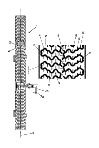
Figure 7 shows a plan view of an element to be deformed in accordance with the
invention;
Figure 8 shows an enlarged detail of Figure 7;
Figure 9 shows a side view of an example of the device in accordance with the
invention;
Figure 10 shows a perspective view of the device of Figure 9;
Figure 11 shows a side view of the device of Figure 9;
Figure 12 shows a section of the device of Figure 11.
The same references in the Figures identify the same or analogous elements or
components.
Detailed description of one preferred embodiment of the invention
With reference to the Figures, a shaping method to plastically deform a
substantially flat flexible conductive element 1 is shown. The flexible
conductive
element 1 may also be called flexible resistive element or flexible resistor
or
flexible flat resistor.
Briefly, a device 11 is provided having an outer surface 12 destined to come
in
contact with the flexible conductive element 1. The flexible conductive
element 1
comprises at least one insulating layer 2 and at least one conductive track 4
fixed
to the insulating layer 2. The device 11 is configured to expand the volume
thereof,
at least radially outwardly.
The method comprises the steps of:
a) arranging the flexible conductive element 1 at least partially around said
device
11, in particular at least partially around and in contact with the outer
surface 12;
5
CA 03044505 2019-05-21
WO 2018/096520 PCT/IB2017/057444
b) expanding the volume of the device 11 up to a predetermined value, whereby
at
least one portion 8 of the flexible conductive element 1 which is in contact
with the
device 11 during the expansion of the device 11 is plastically deformed;
c) separating the deformed flexible conductive element 1 from the device 11.
By way of example, the flexible conductive element 1 is a flexible flat
resistor 1.
Preferably, the at least one insulating layer 2 has a thickness of between 90
and
500 m.
The overall thickness of the flexible flat resistor 1 is preferably of between
0.1 and
1.4 mm, or of between 0.1 and 1.2 mm, or of between 0.1 and 0.8 mm, or of
between 0.2 and 0.8 mm, or of between 0.1 and 0.4 mm, or of between 0.2 and
0.4 mm. Typically, the thickness is much lower than the length and the width
of the
flexible flat resistor 1. For example, the length may be of between 900 and
1200
mm, and the width may be of between 80 and 160 mm, or of between 80 and 100
mm. The flexible flat resistor 1 comprises at least one layer of insulating
material 2
provided, for example above the insulating layer 2, with at least one metal
track or
foil 4, also said resistive track or foil, or conductive track. Preferably,
the flexible
flat resistor 1 comprises only one layer of insulating material 2 which the
metal
track 4 is coupled to. Alternatively, the flexible flat resistor 1 may be
multilayer, in
the sense that it comprises two or more layers of insulating material between
which the metal track is incorporated. In general, the flexible flat resistor
may be
single, or may be formed by the overlapping of two or more insulating layers,
each
provided with at least one respective metal track. For example, a single
flexible flat
resistor is formed by an insulating layer on which the at least one resistive
track is
fastened. According to an example of multilayer flexible flat resistor, a
first
insulating layer is provided, on which the at least one first metal track is
arranged;
on the at least one first metal track and on the first insulating layer a
second
insulating layer is provided, on which at least one second metal track is
provided;
the at least one second metal track may be on the face of the second
insulating
layer, which is proximal to or distal from the at least one first metal track.
Exclusively by way of explanation, the first metal track may be used as
heating
means, and the second metal track may be used as capacitive or resistive
sensor
means.
6
CA 03044505 2019-05-21
WO 2018/096520 PCT/IB2017/057444
Typically, each metal track has a lower superficial extension than the
respective
insulating layer or insulating layers which it is coupled to.
Preferably, the at least one metal track 4 has a width of between 1 and 8 mm.
The support insulating material, i.e. the material of the insulating layer 2,
is
.. typically a polymeric material. Exclusively by way of example and not by
way of
limitation, insulating materials are PVC, PTFE, PS, PP, PE, PC, ABS, PET, PA,
PU (also expanded), PUR, NBR, Silicone, EPDM and the like, optionally with
additives. In general, thermoplastic and elastomeric materials may be used,
which
have suitable elongation capabilities. Preferably, at least one insulating
layer 2 is
provided made of a polymeric non-elastomeric material, preferably a non-
elastomeric and non-silicone material. Preferably, at least one insulating
layer 2 is
provided, made of Polyvinyl chloride or Polystyrene or Polypropylene or
Polyethylene or Polyethylene terephthalate or Polyurethane.
The at least one metal track 4, which may have a complex geometry, is adapted
to
be connected to an electrical power source, typically by means of one or more
connectors 7a, 7b. Exclusively by way of example and not by way of limitation,
materials with which the metal track may be made of are Aluminum, Constantan,
Copper, German Silver, Steel, Inconel, Brass and the like. Preferably, the
metal
track 4 is made of aluminum. Preferably, the metal track 4 has a thickness of
between 10 and 200 m.
The flat resistor is flexible 1, in the sense that the flat resistor 1 may be
elastically
deformed when external forces are applied thereon.
Furthermore, when subjected to a suitable force, the flexible flat resistor 1
may be
deformed by plastic deformation, being subjected for example to a stretching.
.. The method of the invention provides the use of the device 11, also said
shaping
device, having an outer surface 12 destined to come in contact with the
flexible
conductive element 1, or flexible resistor, to obtain the aforesaid plastic
deformation thereof. Such device 11 is configured to expand the volume
thereof, in
particular radially outwardly.
Exclusively by way of explanation, a device 11 adapted to the shaping method
comprises a chamber 14 for a fluid. The chamber 14 is expandable, in
particular
radially outwardly. The aforesaid outer surface 12 of the chamber 14, at least
7
CA 03044505 2019-05-21
WO 2018/096520 PCT/IB2017/057444
when the chamber is expanded, has a predetermined shape, which is
substantially
equal to the shape which is intended to be given to the flexible resistor 1.
Preferably, the shape of such surface 12 is toroidal, or at least partially
toroidal, it
being understood that also shapes different from this one may be provided. In
particular, in the case of a toroidal surface, the outer surface 12 of the
expanded
chamber 14 is curved, more precisely, it is shaped as the outer surface of a
toroid.
Preferably, the radius of curvature is of between 10 and 20 mm, more
preferably of
between 12.5 and 17.5 mm. It is also optionally provided that the shape of the
toroid is elliptic.
Furthermore, it is preferable that the chamber 14 is made of a material
adapted to
elastically deform, for example of an elastomeric material. To expand the
chamber
14, a fluid is entered inside the chamber 14, for example a gas, such as air,
or a
liquid. To this end, the chamber is provided with a specific fluid entrance,
for
example a valve. When the fluid is expelled from the chamber 14 of the device
11,
the chamber 14 reduces the volume thereof, and therefore the volume of the
device 11 is reduced.
The method comprises a step in which the flexible resistor 1 is arranged at
least
partially around the shaping device. The arrangement may be such that the two
ends of the flexible resistor are not in contact with one another
(substantially
forming an open ring) or such that the two ends of the resistor are in contact
with
one another (substantially forming a closed ring). In the latter case, such
ends may
be fastened to one another. For example, the flexible resistor is wrapped
around
the shaping device and then the two edges of opposite ends are overlapped and
secured with one another, for example by means of adhesive means, or by means
of heat sealing, or by means of clamping means such as pliers, whereby a
junction
area 6 is defined (Figure 5).
Furthermore, the arrangement is preferably such that the inner surface,
proximal
to the device 11, of the flexible resistor 1 is in contact with the outer
surface 12 of
the device 11. Alternatively, the inner surface of the flexible resistor 1 may
initially
be separated from the outer surface 12 of the device 11, and the flexible
resistor 1
gets in contact with the device 11 when the latter reaches a predetermined
expansion degree.
8
CA 03044505 2019-05-21
WO 2018/096520 PCT/IB2017/057444
Preferably, but not exclusively, the size of the shaping device 11 is such
that only
a portion 8 (Figure 4) of the width of the flexible resistor 1 is deformed.
For
example, with such dimensioning, only a central portion 8 of the flexible
resistor 1
is deformed, while two side portions 9 remain substantially unchanged. Or a
differentiated elongation may be obtained between the central area and the
side
areas. The width of the resistor typically indicates the dimension which is
lower
with respect to the length.
Subsequently, the volume of the device, in particular of the expandable
chamber,
is expanded in a controlled manner. The expansion of the device 11 is
preferably
carried out until reaching a predetermined deformation value, whereby the
flexible
resistor 1 is deformed according to the design. During the expansion of the
device
11, the portion 8 of flexible resistor 1 which is in contact with the device
11 is
deformed, in particular stretched, plastically.
Optionally, it is preferable to provide deformation control means to prevent
the
expansion of the volume of the device beyond the predetermined value.
According to an embodiment, the deformation control means comprise an
abutment body 21, preferably of a substantially circular shape, arranged
around
the flexible conductive element 1. In particular, it is provided that the
flexible
conductive element 1 is between the device 11 and the abutment body 21. During
the expansion of the device 11, when the flexible conductive element 1 abuts
against the abutment body 21, the expansion of the device 11 is interrupted.
The
interruption may be manual or automatic. The shaping device 11 may have a
frame on which the abutment body 21 is fastened.
Another example of deformation control means is provided by a laser pointer
with
a suitably directed laser beam. Suitable reference marks, to be used in
combination with the laser pointer, may be applied on the flexible resistor.
Preferably, the invention also provides alignment means to suitably position
and/or
center the flexible resistor with respect to the device. Such alignment means
may
be of the mechanical type, for example, one or more plates may be provided.
Alternatively, a laser pointer with a suitably directed laser beam may be
provided,
preferably matching the medial axis of the device, which acts as an optical
guide
for the correct positioning and centering of the flexible resistor. Also in
this case,
9
CA 03044505 2019-05-21
WO 2018/096520 PCT/IB2017/057444
suitable reference marks, to be used in combination with the laser pointer,
may be
applied on the flexible resistor.
Other examples of deformation control means and/or alignment means for
positioning and centering the flexible resistor may be optical, magnetic
and/or
electric and/or capacitive.
Preferably, during the expansion of the device or immediately before or
afterwards, heat is administered to the flexible conductive element 1 so as to
improve the deformation thereof and the keeping of the deformation itself. For
example, the deformation may be improved when the flexible conductive element
1 is heated at a temperature greater than 20 or 25 C, for example of between
60
and 130 C.
The heat may be administered by means of thermoregulation means. For
example, the heat may be administered by means of ovens, means producing a
flow of hot air, or by means of the direct contact with hot surfaces heated
for
example by means of resistive means, or combinations thereof.
Alternatively, or additionally, the fluid may be entered into the expandable
chamber 14 of the device 11 at a temperature greater than 20 or 25 C, for
example of between 60 and 130 C.
In general, adjustment means may be provided which may increase or decrease
the temperature, for example, with respect to 25 C.
In some cases, it may be advantageous that, once the device 11 has reached the
volume predetermined to obtain the desired deformation, the deformed
conductive
element 1 is kept in contact with the expanded device 11 for a predetermined
keeping time. In this way, the final shape of the conductive element 1 is
stabilized.
Furthermore, after the deformation, cooling the deformed conductive element 1
may be advantageous. To this end, natural or forced air convection cooling
means
or cold stores may be provided. The cooling temperature is preferably such to
bring the conductive element back to ambient temperature in a time preferably
lower than 5 minutes.
Exclusively by way of example and not by way of limitation, the following
table
includes possible combinations of process parameters, valid, for example, when
the insulating material is PVC or a similar material.
CA 03044505 2019-05-21
WO 2018/096520 PCT/IB2017/057444
Heating Heating Cooling Cooling
Example Duration Temperature Duration Temperature
[minutes] [ C] [minutes] [ C]
1 2 +60 1 -30
2 1 + 60 2 +
25 (ambient)
3 2 +90 1 -30
4 1 + 90 2 +
25 (ambient)
2 +120 1 -30
6 1 + 120 2 +
25 (ambient)
Once deformed, the flexible conductive element 1 is separated from the device
11.
5 To facilitate the detachment, the chamber 14 of the device 11 is
preferably
emptied, at least partially, of the fluid contained therein.
Figures from 9 to 12 show and example of a device 11 in accordance with the
invention.
The device 11 is shown in the expanded configuration thereof. The flexible
resistor
.. 1 is arranged around the device. A countermold 31 is provided, acting as an
abutment body to control the deformation of the resistor 1. The countermold 31
may be formed by two parts so as to be openable. Although in the described
embodiment a countermold 31 is provided, arranged only on one side of the
center
plane of the device 11, a further complementary countermold may be provided,
.. arranged on the other side of the center plane. The device 11 and the
countermold
31 are connected to respective thermoregulation means 33, 35 which allow to
adjust the temperature thereof, so as to heat up and/or cool down the flexible
resistor 1.
The method of the invention has been designed to obtain a plastic deformation
of
the flexible flat resistor 1. Advantageously, the method allows to obtain a
substantially uniform plastic deformation.
By virtue of the plastic deformation, the flexible resistor 1 is specifically
adapted to
adhere to a complex item, in particular to the steering wheel of an
autovehicle (not
shown). To this end, the deformed portion 8 of flexible resistor 1 is, in
fact, shaped
.. so as to be curved, so as to have a curvature substantially similar or
equal to that
11
CA 03044505 2019-05-21
WO 2018/096520 PCT/IB2017/057444
of the steering wheel, in particular to the torus of the steering wheel.
Preferably,
the radius of the torus of the deformed surface is of between 10 and 20 mm,
more
preferably of between 12.5 and 17.5 mm.
The deformed flexible resistor 1 may optimally coat the torus of the steering
wheel,
without formation of creases or ripples.
According to an aspect, the invention also provides a steering wheel coated
with
the resistor deformed by the method of the invention.
According to an embodiment, a flexible resistor is produced with an insulating
layer 2 in PVC above which at least one metal track 4 is fixed. The face of
the
.. insulating layer 2 provided with the metal track 4 is arranged in contact
with the
outer surface of the steering wheel. The opposite face of the insulating layer
is
preferably coated with a steering wheel coating material, for example, natural
or
synthetic leather, on which a person may place the hands. The at least one
metal
track is used to heat the steering wheel. The metal track may also be used as
a
.. sensor.
According to another embodiment, a sandwich structure is provided, formed by
two insulating layers, preferably made of PVC, between which at least one
conductive track is arranged, for example, one or two conductive tracks. In
this
case, it is preferable that each PVC layer has a thickness of between 100 and
300
m, for example, of about 200 m. It is further preferable that the conductive
track,
or the conductive tracks, have a thickness of between 10 and 200 m, for
example
of about 60 m.
An embodiment not shown provides for an insulating layer with a resistive
track for
the heating, and a track acting as a capacitive or resistive sensor.
The invention also provides a flexible resistor 1 which, not only is improved
with
respect to the state of the art, but is also particularly adapted to be
deformed by
the method of the invention. In fact, to this end, it is preferred to select
designs, or
shapes, of the metal track 4 which allow deformations of the flexible resistor
in the
three dimensions without interruptions or mechanical breakages, not even
partial,
occurring on the metal track. To this end, it is preferred that the overall
percentage
of metal track stretches parallel to the main deformation axis of the flexible
resistor
1 is lower than 50% with respect to the total number of metal track stretches.
The
12
CA 03044505 2019-05-21
WO 2018/096520 PCT/IB2017/057444
main deformation axis is preferably the longitudinal axis X of the flexible
flat
resistor. For example, some stretches parallel to the main deformation axis X
are
indicated with reference number 3' in Figure 8.
Additionally, or alternatively to such feature related to the orientation of
the
.. stretches 3, it is preferred that resistive track stretches 3 adjacent to
one another,
having different directions from one another, are joined to one another with
radii of
curvature greater than 0.5 mm, preferably greater than 1 mm, even more
preferably greater than 2 mm.
Typically, the invention provides that the metal track 4, or metal tracks,
have a
relatively complex shape. For example, each metal track 4 may have a
substantially serpentine shape. The serpentine is formed by a plurality of
stretches
3, or portions, oriented and joined as described above.
Preferably, each metal track 4 is provided with a plurality of branches 5 or
side
extensions, typically designed so as not to be crossed by electric current. As
current does not flow in such branches 5, the branches do not heat up, since
the
current tends to pass where it encounters less resistance, i.e., in the
resistive
track. The function thereof is to act as dissipating fins, which contribute to
better
uniform and disperse the thermal flow generated by the electric current
running
through the resistive track 4 on the surface of the flexible resistor. The
branches 5
are preferably made of the same material which the resistive track 4 is made
of,
and, preferably, the branches 5 are integral with the respective resistive
track 4.
Preferably, each branch 5 is substantially rectilinear.
Preferably, the material of the insulating layer 2 allows a stretching
deformation of
at least 15%, preferably of at least 30%. It is further preferred that the
overall
thickness of the flexible flat resistor 1 is of between 0.1 and 1.4 mm, or of
between
0.1 and 1.2 mm, or of between 0.1 and 0.8 mm, or of between 0.2 and 0.8 mm, or
of between 0.1 and 0.4 mm, or of between 0.2 and 0.4 mm.
A material particularly apt to be the insulating layer is PVC, preferably
containing
additives and/or plasticizes.
In general, exclusively by way of example, the process described below may be
followed to produce flexible flat resistors 1.
13
CA 03044505 2019-05-21
WO 2018/096520 PCT/IB2017/057444
One or more sheets of insulating material are passed with a sheet of
conductive
material between two rollers. The sheets are thus coupled to one another. At
least
one metal track and possible branches are designed on the conductive sheet,
for
example by means of photoresist. The parts of the conductive sheet which are
not
part of the track are then removed, for example by means of chemical etching.
Alternatively, the conductive track is made by means of screen printing, or
printing,
or by deposition of one or more conductive inks on the insulating layer,
whereby
the conductive track comprises or is formed by conductive ink.
14