Note: Descriptions are shown in the official language in which they were submitted.
SOLAR CELL AND SOLAR CELL MODULE
TECHNICAL FIELD
[0001] The present invention relates to afield of photovoltaic(PV)
technology,
and in particular to a solar cell and a solar cell module.
BACKGROUND
[0002] The adjacent solar cells in a shingled module are partially
overlapped
with each other and bonded by a special conductive adhesive. Compared with a
113 traditional PV module, the shingled module can make full use of light-
receiving areas
of the solar cells. The shingled module which has a same dimension with the
traditional PV module can hold more solar cells and does not use solder strips
to
connect adjacent solar cells. Thus, the shingled module has high efficiency
and low
loss.
[0003] During the manufacturing process of a conventional shingled module,
a
front edge electrode of a solar cell and a rear edge electrode of an adjacent
solar cell
are bonded and electrically connected through a conductive adhesive. However,
the
above connection method requires high bonding strength and electrical
conductivity
between the bus bars and the conductive adhesive. As a result, the raw
material cost
of the shingled module is kept high correspondingly. Thus, not only the
composition
of the conductive adhesive is required to be adjusted and improved in the
industry,
but also the bus bars of the solar cells need to be optimally designed to
reduce the
production cost and improve the performance of the shingled module.
SUMMARY
[0004] In view of this, the present invention provides a solar cell
and a solar
cell module, in order to enhance the bonding strength of adjacent solar cells,
reduce
the internal loss and improve the power generation efficiency.
[0005] According to an aspect of the present invention, a solar cell
includes a
plurality of rectangular unit regions, each of which having a front
metallization
pattern on a front surface of the unit region and a rear metallization pattern
on a rear
surface of the unit region, wherein each of the front metallization pattern
and rear
CA 3044596 2019-05-29
3152148 1
,
metallization pattern comprises an elongated edge electrode, and the elongated
edge
electrode of the front metallization pattern and the elongated edge electrode
of the
rear metallization pattern located at two opposite edges of each unit region,
respectively. At least one portion of the edge electrode comprises two
paralleled bus
bars with an unpatterned region formed therebetween for receiving adhesive
material.
[0006] According to another aspect of the present invention, a solar
cell
includes a rectangular semiconductor substrate having a front surface and a
rear
surface opposite to the front surface, and a front metallization pattern
formed on the
front surface and a rear metallization pattern formed on the rear surface,
wherein each
of the front metallization pattern and rear metallization pattern comprises an
elongated edge electrode, and the elongated edge electrode of the front
metallization
pattern and the elongated edge electrode of the rear metallization pattern
located at
two opposite edges of the semiconductor substrate, respectively. At least one
portion
of the edge electrode comprises two paralleled bus bars with an unpatterned
region
formed therebetween for receiving adhesive material.
[0007] The present invention further provides a solar cell module,
which
includes a plurality of solar cell strings arranged in two or more parallel
rows. Each
solar cell string having a plurality of rectangular solar cells arranged in
line with
adjacent solar cells partially overlapped and conductively bonded to each
other by
.. adhesive material. Each solar cell has a front metallization pattern on a
front surface
of the solar cell and a rear metallization pattern on a rear surface of the
solar cell.
Each of the front metallization pattern and rear metallization pattern
comprises an
elongated edge electrode, and the elongated edge electrode of the front
metallization
pattern and the elongated edge electrode of the rear metallization pattern
located at
two opposite edges of the solar cell, respectively. At least one portion of
the edge
electrode comprises two paralleled bus bars with an unpatterned region formed
there
between for receiving adhesive material
BRIEF DESCRIPTION OF THE DRAWINGS
[0008] The components in the drawing are not necessarily drawn to scale,
the
emphasis instead being placed upon clearly illustrating the principles of the
described
embodiments. In the drawings, reference numerals designate corresponding parts
throughout various views, and all the views are schematic.
CA 3044596 2019-05-29
3152148 2
[0009] FIG. 1 is a schematic view of a front side of a solar cell
according to
the present invention;
[0010] FIG. 2 is a schematic view of a rear side of the solar cell
shown in FIG.
1;
[0011] FIG. 3 is an enlarged schematic view of the region A shown in FIG.
1;
[0012] FIG. 4 is a schematic view of a front side of a solar cell
according to
another embodiment of the present invention;
100131 FIG. 5 is a schematic view of a rear side of the solar cell
shown in FIG.
4;
[0014] FIG. 6 is an enlarged schematic view of the region B shown in FIG.
4.
DETAILED DESCRIPTION
[0015] Exemplary embodiments will be described in detail herein,
examples of
which are illustrated in the accompanying drawings. The following description
refers
to the accompanying drawings in which the same numbers in different drawings
represent the same or similar elements unless otherwise indicated. The
implementations set forth in the following exemplary embodiments do not
represent
all implementations consistent with the present invention. Rather, they are
merely
examples of devices and methods consistent with certain aspects of the present
invention as detailed in the appended claims.
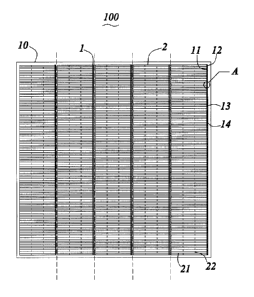
[0016] Please refer to Figs. 1-3, the present invention provides a
solar cell 100
which includes a plurality of rectangular unit regions 10. The unit regions 10
are
sequentially arranged adjacent to one another, and each of which having a
front
metallization pattern on a front surface of the unit region 10 and a rear
metallization
pattern on a rear surface of the unit region 10. Here, there are 2-8 unit
regions 10 in
the solar cell 100, and each unit region 10 has two edges which are opposite
and
extend in a first direction.
[0017] Each of the front metallization pattern and rear metallization
pattern
comprises an elongated edge electrode at the two opposite edges of each unit
region
10. That is, the edge electrode extends in the first direction. At least one
portion of
the edge electrode comprises two paralleled bus bars with an unpatterned
region
formed therebetween for receiving adhesive material, wherein the width of the
unpatterned region is greater than the width of the bus bar.
CA 3044596 2019-05-29
3152148 3
[0018] Specifically, the front metallization pattern comprises an
front edge
electrode 1 at one edge of each unit region 10, and the rear metallization
pattern
comprises an rear edge electrode 3 at the opposite edge of each unit region
10.
Wherein all the front edge electrodes 1 of the plurality of unit regions 10
are parallel
located and equally spaced. During actual production, the unit regions 10 are
separated and overlapped one by one through a conductive adhesive, then a
solar cell
string is obtained for preparing a solar cell module. Wherein the conductive
adhesive
is in contact with the front and rear edge electrodes 1, 3.
[0019] In this embodiment, the front edge electrode 1 includes a
first front bus
.. bar 11 and a second front bus bar 12 disposed close to each other, and a
first
unpatterned region 13 between the first and second front bus bars 11, 12. The
first
and second front bus bars 11, 12 extend from one end to another end of the
front
metallization pattern, and the first unpatterned region 13 is used for filling
the
conductive adhesive.
[0020] The rear edge electrode 3 includes a first rear bus bar 31 and a
second
rear bus bar 32 disposed close to each other, and a second unpatterned region
33
between the first and second rear bus bars 31, 32. The first and second rear
bus bars
31, 32 extend from one end to another end of the rear metallization pattern,
and the
second unpatterned region 33 is used for filling the conductive adhesive, too.
[0021] Thereby, when the adjacent unit regions 10 are partially overlapped
with each other, the first and second unpatterned regions 13, 33 can increase
the
contact area between the conductive adhesive and the edge electrode 1, 3, then
the
bonding strength and the electrical connectivity of the front edge electrode 1
to the
rear edge electrode 3 are improved.
[0022] Besides, the front metallization pattern is provided with a
plurality of
finger electrodes 2 perpendicularly connecting with the front edge electrode
1. The
finger electrodes 2 are configured to collect the surface current of the unit
region 10,
and include a plurality of first finger electrodes 21 and a plurality of
second finger
electrodes 22. The first finger electrodes 21 extend in a second direction
perpendicular to the first direction and are parallel to each other. The first
finger
electrodes 21 are connected to the front edge electrode 1 at the same ends.
The
second finger electrodes 22 are connected between adjacent first finger
electrodes 21
so as to collect the current more effectively. The second finger electrodes 22
are
CA 3044596 2019-05-29
3152148 4
parallel to the front edge electrode 1, and adjacent second finger electrodes
22 in the
first direction are staggered with each other.
100231 In order to improve the electrical connection between the
first front bus
bar 11 and the second front bus bar 12 and guarantee stable and uniform
current
conduction, the finger electrodes 2 further include a plurality of
interconnecting
finger electrodes 14 which extend through the first and second front bus bars
11, 12.
The interconnecting finger electrodes 14 are located in the first unpatterned
region 13,
and connect the first front bus bar 11 and the second front bus bar 12 in the
second
direction. Wherein the height of the interconnecting finger electrodes 14 are
smaller
than those of the first front bus bar 11 and the second front bus bar 12, and
the
interconnecting finger electrodes 14 are disposed corresponding to the first
finger
electrodes 21.
100241 The first unpatterned region 13 and the second unpatterned
region 33
have a same shape and correspond to each other in position. During overlapping
of
the unit regions 10, the first unpatterned region 13 and the second
unpatterned region
33 form an accommodating cavity for accommodating the conductive adhesive,
such
that the bonding strength and the electrical connectivity between the front
edge
electrode 1 and the rear edge electrode 3 are improved effectively.
100251 In the present embodiment, the first unpatterned region 13 and
the
second unpatterned region 33 extend linearly in the first direction. Besides,
the first
unpatterned region 13 and the second unpatterned region 33 can be closed at
two ends
thereof, that is the first front bus bar 11 and the second front bus bar 12
being
connected to each other at two ends thereof, and the first rear bus bar 31 and
the
second rear bus bar 32 being connected to each other at two ends thereof.
100261 Referring to Figs. 4-6, in another embodiment of the present
invention,
a solar cell 100' includes a plurality of unit regions 10'. Each of the front
metallization pattern and rear metallization pattern comprises an elongated
edge
electrode at the two opposite edges of each unit region 10'. A portion of the
edge
electrode comprises two paralleled bus bars with an unpatterned region formed
therebetween for receiving adhesive material, and another portion of the edge
electrode comprises only one bus bar which connects with the two paralleled
bus bars.
Wherein the portions of the edge electrode with only one bus bar have a length
which
is shorter than the portions of the edge electrode with two paralleled bus
bars.
CA 3044596 2019-05-29
3152148 5
[0027] The front metallization pattern comprises an front edge
electrode 1' and
a plurality of finger electrodes 2' connected to the front edge electrode 1',
and the
rear metallization pattern comprises an rear edge electrode 3'.
[0028] A portion of the front edge electrode 1' comprises one first
front bus
bar 11', one second front bus bar 12', and one first unpatterned region 13'
between
the first and second front bus bars 11', 12'. Another portion of the front
edge
electrode l' comprises a third front bus bar 15' connected with the two
paralleled bus
bars 11', 12'.
[0029] Wherein the width of the unpatterned region is 13' greater
than the
width of the first and second front bus bars 11', 12'. Preferably, the third
front bus
bar 15' has a width a, the first front bus bar 11' has a width b, the second
front bus
bar 12' has a width c, and the first unpatterned region 13' has a width d,
wherein said
a<b+c+d. Here, the first unpatterned region 13' is preferably closed at two
ends
thereof. The width of the third front bus bar 15' is equivalent to those of
the first
front bus bar 11' and the second front bus bar 12'.
[0030] Similarly, a portion of the rear edge electrode 3' comprises
one first
rear bus bar 31', one second rear bus bar 32', and one second unpatterned
region 33'
between the first and second rear bus bars 31', 32'. The first and second
unpatterned
regions 13' ,33' are arranged into several rows which are perpendicular to the
first
direction, and the first unpatterned regions 13' on the front surface of a
unit region 10'
are arranged corresponding to the second unpatterned regions 33' on the rear
surface
of another unit region 10'.
[0031] The finger electrodes 2' include a plurality of first finger
electrodes 21'
and a plurality of second finger electrodes 22'. The first finger electrodes
21' and the
second finger electrodes 22' are similar to that in the first embodiment and
will not
be detailly described.
[0032] The finger electrodes 2' further include a plurality of
interconnecting
finger electrodes 14' connecting the first front bus bar 11' and the second
front bus
bar 12' in the second direction, and the interconnecting finger electrodes 14'
are
disposed corresponding to the first finger electrodes 21.
[0033] The present invention further provides a solar cell module
(not shown),
includes a plurality of solar cell strings arranged in two or more parallel
rows. Each
solar cell string having a plurality of rectangular solar cells arranged in
line with
CA 3044596 2019-05-29
3152148 6
adjacent solar cells partially overlapped and conductively bonded to each
other by
adhesive material. Specially, solar cell string comprises a plurality of unit
regions 10,
10'. The plurality of unit regions 10, 10' sequentially overlap end to end in
a second
direction, and bonded to each other by a conductive adhesive.
[0034] In summary, The front edge electrode 1, 1' and the rear edge
electrode
3, 3' have been optimally designed. Thus, the consumption of paste used to
prepare
the edge electrodes is reduced and the demand on the performance of the
conductive
adhesive required is lowered, meanwhile, the bonding strength of adjacent unit
regions 10, 10' is higher, and the electrical connection is more reliable.
[0035] It should be understood that although the description is described
according to the above embodiments, each embodiment may not only include one
independent technical solution. The presentation manner of the description is
only for
the sake of clarity. Those skilled in the art should take the description as
an integral
part. The technical solutions of the respective embodiments may be combined
properly to form other embodiments understandable by those skilled in the
field.
[0036] The above detailed description only illustrates the feasible
embodiments of the present invention, and is not intended to limit the
protection
scope of the present invention. Equivalent embodiments or modifications within
the
scope and spirit of the present invention shall be embraced by the protection
scope of
the present invention.
CA 3044596 2019-05-29
3152148 7