Note: Descriptions are shown in the official language in which they were submitted.
4
CA 03044660 2019-05-22
1
Description
Title of Invention
INFORMATION PROCESSING DEVICE AND INFORMATION PROCESSING
METHOD
Technical Field
[0001]
The present disclosure relates to an information processing device and an
information processing method.
Background Art
[0002]
Recently, mathematical models called neural networks that resemble the
workings of neural systems are receiving attention. Also, various techniques
for
reducing the processing load of computations in a neural network are being
proposed.
For example, Non-Patent Literature 1 describes a technique of reducing the
processing load by making weight coefficients binary. Also, Non-Patent
Literature
2 describes a technique of converting multiplication to addition by converting
an
input signal to a logarithmic domain.
Citation List
Non-Patent Literature
[0003]
Non-Patent Literature 1: Matthieu Courbariaux et al., "BinaryConnect:
Training Deep Neural Networks with binary weights during propagations",
[online],
November 11, 2015, arXiv, [retrieved March 22, 2017], Internet <URL:
https://arxiv.org/pdf/1511.00363.pd
Non-Patent Literature 2: Daisuke Miyashita et al., "Convolutional Neural
Networks using Logarithmic Data Representation", [online], March 3, 2016,
arXiv,
[retrieved March 22, 2017], Internet <URL:
https://arxiv.org/pdf/1603.01025.pdf>
4
CA 03044660 2019-05-22
2
Disclosure of Invention
Technical Problem
[0004]
However, with the technique described in Non-Patent Literature 1, since
binarization using +1 or -1 is performed, the quantization granularity is
expected to
become rougher as the dimensionality of the weight coefficients increases.
Also,
the technique described in Non-Patent Literature 2, although having a
predetermined
effect in the avoidance of multiplication, is anticipated to have room for
further
improvement in the reduction of the processing load.
[0005]
Accordingly, the present disclosure proposes a novel and improved
information processing device and information processing method capable of
further
reducing the processing load associated with inner product operations while
also
guaranteeing the quantization granularity of weight coefficients.
Solution to Problem
[0006]
According to the present disclosure, there is provided an information
processing device including: a multiply-accumulate operation circuit
configured to
execute a multiply-accumulate operation on the basis of multiple input values
and
multiple weight coefficients that are quantized by an exponential
representation and
that correspond to each of the input values. Exponents of the quantized weight
coefficients are expressed by fractions taking a predetermined divisor as a
denominator, and the multiply-accumulate operation circuit performs the
multiply-
accumulate operation using different addition multipliers on the basis of a
remainder
determined from the divisor.
[0007]
Moreover, according to the present disclosure, there is provided an
information processing method, executed by a processor, including: executing a
multiply-accumulate operation on the basis of multiple input values and
multiple
CA 03044660 2019-05-22
3
weight coefficients that are quantized by an exponential representation and
that
correspond to each of the input values. Exponents of the quantized weight
coefficients are expressed by fractions taking a predetermined divisor as a
denominator, and the executing of the multiply-accumulate operation performs
the
multiply-accumulate operation using different addition multipliers on the
basis of a
remainder determined from the divisor.
Advantageous Effects of Invention
[0008]
According to the present disclosure as described above, it becomes possible
to further reduce the processing load associated with inner product operations
while
also guaranteeing the quantization granularity of weight coefficients.
[0009]
Note that the effects described above are not necessarily limitative. With
or in the place of the above effects, there may be achieved any one of the
effects
described in this specification or other effects that may be grasped from this
specification.
Brief Description of Drawings
.. [0010]
[FIG I] FIG 1 is a conceptual diagram for explaining an overview of basic
computations in a neural network according to a related technology of the
present
disclosure.
[FIG. 2] FIG. 2 is an overview diagram for explaining an inner product
operation of
an input vector and a weight vector according to a related technology of the
present
disclosure.
[FIG. 3] FIG 3 is a diagram for explaining a binary-quantized weight vector in
a two-
dimensional space according to a related technology of the present disclosure.
[FIG. 4] FIG. 4 is a diagram for explaining a quaternary-quantized weight
vector in a
two-dimensional space according to a related technology of the present
disclosure.
[FIG. 5] FIG. 5 is a diagram for explaining discrepancies in the granularity
of a
CA 03044660 2019-05-22
4
weight vector in a three-dimensional space according to a related technology
of the
present disclosure.
[FIG 6] FIG 6 is a diagram for explaining discrepancies in the granularity of
a
weight vector in an N-dimensional space according to a related technology of
the
present disclosure.
[FIG. 7] FIG 7 is one example of a function block diagram of an information
processing device according to one embodiment of the present disclosure.
[FIG 8] FIG 8 is one example of a circuit block diagram of a multiply-
accumulate
operation circuit provided in the information processing device according to
the
embodiment.
[FIG. 9] FIG 9 is one example of an offset notation for address information
stored in
an address table according to the embodiment.
[FIG. 10] FIG. 10 is a diagram illustrating a process representation of the
information
processing method according to the embodiment.
[FIG. 11] FIG. 11 is a diagram for explaining a quantization granularity AO
according
to the embodiment.
[FIG 12] FIG. 12 is a graph illustrating a maximum value of the quantization
granularity AO according to a according to the embodiment.
[FIG 13] FIG 13 is a diagram for explaining a maximum exponent according to
the
embodiment.
[FIG. 14] FIG 14 is a diagram illustrating an example of the number of times
of
multiplications with respect to the number of inputs N according to the
embodiment.
[FIG 15] FIG. 15 is a diagram illustrating an example of the number of times
of
multiplications with respect to the number of inputs N according to the
embodiment.
[FIG. 16] FIG. 16 is one example of the multiply-accumulate operation circuit
in a
case of quantizing the weight vectors according to a second embodiment of the
present disclosure.
[FIG. 17] FIG. 17 is one example of the multiply-accumulate operation circuit
in a
case of quantizing both the weight vectors and the input vectors according to
the
same embodiment.
[FIG. 18] FIG. 18 is one example of the multiply-accumulate operation circuit
in a
CA 03044660 2019-05-22
case of quantizing both the weight vectors and the input vectors according to
the
same embodiment.
[FIG. 19] FIG 19 is a diagram illustrating a network structure of a ResNet
used in a
comparative experiment according to the same embodiment.
5 [FIG. 20] FIG 20 is a diagram illustrating a ResNet network configuration
that does
not include a Max Pooling layer according to the same embodiment.
[FIG. 21] FIG. 21 is a diagram illustrating a ResNet network configuration
that
includes a Max Pooling layer according to the same embodiment.
[FIG. 22] FIG. 22 is a diagram illustrating a result of comparing image
recognition
rate according to the same embodiment.
[FIG. 23] FIG. 23 is a diagram illustrating a simulation result according to
frequency
characteristics (gain characteristics) when the quantization technique
according to the
same embodiment is applied to a bandpass filter.
[FIG. 24] FIG 24 is a diagram illustrating a simulation result according to
phase
characteristics when the quantization technique according to the same
embodiment is
applied to a bandpass filter.
[FIG. 25] FIG 25 is a block diagram utilized in BER evaluation according to
the
same embodiment.
[FIG. 26] FIG 26 is a diagram illustrating a BER evaluation result when using
BPSK
according to the same embodiment for the modulation method.
[FIG. 27] FIG 27 is an enlarged view of the data of the SNR from 7 to 9 dB in
FIG
26.
[FIG 28] FIG. 28 is a diagram illustrating a BER evaluation result when using
QPSK
according to the same embodiment for the modulation method.
[FIG. 29] FIG. 29 is an enlarged view of the data of the SNR from 10 to 12 dB
in FIG.
28.
[FIG. 30] FIG 30 is a diagram illustrating a BER evaluation result when using
16QAM according to the same embodiment for the modulation method.
[FIG. 31] FIG. 31 is an enlarged view of the data of the SNR from 16 to 18 dB
in FIG.
30.
[FIG. 32] FIG 32 is a diagram illustrating an exemplary hardware configuration
CA 03044660 2019-05-22
6
according to one embodiment of the present disclosure.
Mode(s) for Carrying Out the Invention
[0011]
Hereinafter, (a) preferred embodiment(s) of the present disclosure will be
described in detail with reference to the appended drawings. Note that, in
this
specification and the appended drawings, structural elements that have
substantially
the same function and structure are denoted with the same reference numerals,
and
repeated explanation of these structural elements is omitted.
[0012]
Hereinafter, the description will proceed in the following order.
1. Embodiment
1.1. Background
1.2. Exemplary functional configuration of information processing
device 10
1.3. Weight vector quantization
1.4. Exemplary configuration of multiply-accumulate operation
circuit
1.5. Quantization during learning
1.6. Effects
2. Second embodiment
2.1. Overview
2.2. Quantization of weight vectors
2.3. Quantization of both weight vectors and input vectors
2.4. Effects
2.5. Example of application to communication technology
3. Exemplary hardware configuration
4. Conclusion
[0013]
<1. Embodiment>
<<1.1. Background>>
4
CA 03044660 2019-05-22
7
Recently, learning techniques using neural networks, such as deep learning,
are being researched widely. Although learning techniques using neural
networks
are highly accurate, because of the large processing load associated with
computation,
there is demand for computational methods that reduce the processing load
effectively.
[0014]
For this reason, in recent years, computational methods that aim to reduce
the amount of computation and the amount of information, such as binary weight
networks and XNMOR nets, for example, have also been proposed.
[0015]
Herein, an overview of basic computations in a typical neural network will
be described. FIG 1 is a conceptual diagram for explaining an overview of
basic
computations in a neural network. FIG. 1 illustrates two layers forming the
neural
network, and cells cli to clN and a cell c2i belonging to each of the two
layers.
[0016]
At this point, the input signal (hereinafter also designated the input vector)
input into the cell C21 is decided on the basis of the input vector and weight
coefficients (hereinafter also designated the weight vector) associated with
the cells
cli to c 1N belonging to the lower layer. More specifically, the input vector
input
into the cell c2i becomes a value obtained by adding a bias b to the result of
an inner
product operation of the input vector and the weight vector associated with
the cells
cli to cl N, and additionally processing by an activation function h.
[0017]
In other words, in the case of taking x=(xl, X2, X3, ... XN) and w=(wi, w2,
w3, wN) to be each of the input vector and the weight vector associated with
the
cells cli to c1N, an input vector z input into the cell c2i is defined by the
following
Formula (1).
[0018]
[Math. 1]
CA 03044660 2019-05-22
8
Z = 1/(1 xiwi + b) . . . ( 1)
[0019]
At this point, assuming a hyperplane h whose normal is the weight vector w,
as illustrated in FIG 2, the inner product of the input vector x and the
weight vector
w expressed in N dimensions can be expressed as the value obtained by
multiplying
iiwii by a projection distance d of projecting the input vector x onto the
weight vector
w based on the hyperplane h. Herein, the above Ilwil is the norm of the vector
w.
FIG. 2 is an overview diagram for explaining the inner product operation of
the input
vector x and the weight vector w.
[0020]
At this point, in the case in which the input vector x and the weight vector w
are two-dimensional, if the weight vector w is quantized into a binary value
of +1 or
-1 like in Non-Patent Literature 1, the weight vector w can be represented as
in FIG
3. FIG. 3 is a diagram for explaining the binary-quantized weight vector w in
a
two-dimensional space. At this point, the granularity of the weight vector w
can be
expressed by a rotational angle 0 in the plane, and as illustrated in FIG 3,
the
granularity becomes 90 degrees.
[0021]
Next, consider the case of quantizing the weight vector w into the
quaternary values of {0, 1/4, 1/2, 1}. FIG 4 is a diagram for explaining the
quaternary-quantized weight vector w in a two-dimensional space. In this case,
the
granularity of the weight vector w, or in other words the rotational angle 0,
becomes
approximately 15 degrees, making it possible to guarantee a finer granularity
compared to the case of binary quantizing.
[0022]
On the other hand, discrepancies in the granularity of the weight vector w
are expected to become larger as the dimensionality increases. FIG 5 is a
diagram
for explaining discrepancies in the granularity of the weight vector w in a
three-
dimensional space. For example, as illustrated in FIG. 5, in the case of
considering
CA 03044660 2019-05-22
9
the quantizing of the weight vector w in a plane defined by (1, 1, 0) and (0,
0, 1), the
length of the side in the (1, 1, 0) direction becomes the length of the side
in the (0, 0,
1) direction multiplied by the square root of 2, thereby demonstrating that
discrepancies in the granularity during quantization increase.
[0023]
Also, these discrepancies, or in other words non-uniformity, of the
granularity like the above become more prominent as the dimensionality
increases.
FIG. 6 is a diagram for explaining discrepancies in the granularity of the
weight
vector w in an N-dimensional space. FIG 6 illustrates a plane defined by (1,
1, ..., 1,
0) and (0, 0, ..., 0, I) in an N-dimensional space. In this case, the length
of the side
in the (1, 1, ..., 1, 0) direction can be expressed by the length of the side
in the (0,
0, ..., 0, 1) direction multiplied by the square root of (N-1). For example,
in the case
of N=100, the length of the side in the 1, I, ..., 1, 0) direction becomes the
length of
the side in the (0, 0, ..., 0, 1) direction multiplied by the square root of
99 (1 0).
[0024]
Since non-uniformity in the granularity associated with the weight vector w
as above may be a factor causing a performance drop in a neural network, a
more
accurate quantization technique is desired. The technical idea according to
the
present disclosure was conceived by focusing on the above point, and makes it
possible to reduce the processing load effectively while also maintaining high
accuracy in the approximation of a weight vector in an N-dimensional space.
For
this reason, one feature of the information processing device and information
processing method according to the first embodiment of the present disclosure
is to
execute an inner product operation using a weight vector quantized on the
basis of
the granularity of a vector direction in an N-dimensional hypersphere plane.
The
information processing device and information processing method according to
the
first embodiment of the present disclosure are capable of achieving both high
approximation accuracy and a reduction in the processing load by quantizing
the
weight vector with a granularity that is not too fine and not too coarse. More
specifically, the information processing device and information processing
method
according to the first embodiment of the present disclosure preferably
executes an
CA 03044660 2019-05-22
inner product operation using a weight vector expressed by exponentiation.
Hereinafter, the above features included in the information processing device
and the
information processing method according to the first embodiment of the present
disclosure will be described in detail.
5 [0025]
<<1.2. Exemplary functional configuration of information processing device
10>>
Next, an exemplary functional configuration of the information processing
device 10 that realizes the information processing method according to the
present
embodiment will be described. FIG. 7 is one example of a function block
diagram
10 of the information processing deice 10 according to the present
embodiment.
Referring to FIG. 7, the information processing device 10 according to the
present
embodiment is provided with an input unit 110, a computation unit 120, a
storage
unit 130, and an output unit 140. Hereinafter, the description of the above
configuration will focus on the functions included in the configuration.
[0026]
(Input unit 110)
The input unit 110 according to the present embodiment has a function of
detecting various types of input operations by an operator. For this reason,
the input
unit 110 according to the present embodiment preferably includes various
devices for
.. detecting input operations by the operator. For example, the input unit 110
may be
realized by any of various types of buttons, a keyboard, a touch panel, a
mouse, a
switch, and the like.
[0027]
(Computation unit 120)
The computation unit 120 has a function of performing inner product
operations based on multiple input values and multiple weight coefficients
corresponding to each of the input values, and computing an output value.
Particularly, the computation unit 120 according to the present embodiment
performs
inner product operations associated with the forward propagation of a neural
network.
At this point, one feature of the computation unit 120 according to the
present
embodiment is to compute an output value on the basis of weight coefficients
CA 03044660 2019-05-22
11
quantized on the basis of the granularity of a vector direction on an N-
dimensional
hypersphere surface. More specifically, the computation unit 120 according to
the
present embodiment preferably computes an output value on the basis of weight
coefficients expressed by exponentiation. The features of the inner product
.. operations in the present embodiment will be described separately later.
[0028]
(Storage unit 130)
The storage unit 130 has a function of storing programs, data, and the like
used by each configuration element provided in the information processing
device 10.
For example, the storage unit 130 according to the present embodiment stores
various parameters and the like used in a neural network.
[0029]
(Output unit 140)
The output unit 140 has a function of outputting various information to the
operator. For this reason, the output unit 140 according to the present
embodiment
may include a display device that outputs visual information. Herein, the
above
display device may be realized by a cathode ray tube (CRT) display device, a
liquid
crystal display (LCD) device, an organic light-emitting diode (OLED) device,
or the
like, for example.
.. [0030]
The above describes an exemplary functional configuration of the
information processing device 10 according to the present embodiment. Note
that
the exemplary functional configuration described above is merely one example,
and
the exemplary functional configuration of the information processing device 10
.. according to the present embodiment is not limited to such an example. The
information processing device 10 according to the present embodiment may also
be
provided additionally with configuration elements other than those illustrated
in FIG
1. For example, the information processing device 10 may be provided
additionally
with a communication unit that communicates information with another
information
processing terminal, and the like. The functional configuration of the
information
processing device 10 according to the present embodiment may be flexibly
changed
CA 03044660 2019-05-22
12
in design.
[0031]
<<1.3. Weight vector quantization>>
Next, the quantization of weight vectors according to the present
embodiment will be described in detail. As described above, the information
processing device 10 according to the present embodiment is able to maintain
highly
uniform granularity by executing quantization with weight vectors w expressed
by
exponentiation. At this point, one feature of the computation unit 120
according to
the present embodiment is to reorder multiple weight vectors component vw, in
order
of smallest value, and also normalize the multiple weight vectors component w,
by
the weight coefficient w, with the largest value. At this point, if the
reordered and
normalized weight vectors are taken to be wj, the weight vectors wj are
indicated by
the following Formulas (2) to (4).
[0032]
[Math. 2]
w =s an' (j <N) = = = ( 2 )
1 1
W =1
. . . 3)
. ( 4 )
[0033]
However, at this point, in the above Formula (2), a preferably is 0<a<1, sj
preferably is an element of the set {-1, 1}, and nj preferably is an element
of the set
{0, 1, 2, ...}. In other words, the computation unit 120 according to the
present
embodiment performs quantization treating nj as integers. In this case, the
inner
product operation executed by the computation unit 120 is indicated by the
following
Formula (5). Note that in the following Formula (5), K denotes a normalization
constant. Also, it is sufficient for the value of a above to fall ultimately
within the
above range in the inner product operation, even in the case of appropriately
transforming the following Formula (5). The formulas illustrated in the
present
disclosure are merely one example, and may be flexibly transformed.
CA 03044660 2019-05-22
13
[0034]
[Math. 3]
K((...(s1xian1-n2 + s2x2)an'n3 + s3x3)an3-n4 +...)a'7' + sNxN),
K E R = = = ( 5 )
[0035]
For this reason, the inner product operation by the computation unit 120
according to the present embodiment is expected to be processable by N
addition
operations and the number of times of multiplications on the order of -1/2 log
(N-
1)/log a.
[0036]
In this way, one feature of the information processing method according to
the present embodiment is to approximate the weight vectors w by an
exponential
representation of a, and reorder the weight vectors w in order of smallest
value. At
this point, in the information processing method according to the present
embodiment, by converting the exponents of a to t-ary values according to N,
the
weight vectors w are quantized.
[0037]
For example, for the case in which N=100, in the information processing
method according to the present embodiment, t=4 (2-bit), 8 (3-bit), 16 (4-bit)
or the
like may be adopted. By setting t as above, since most of ni -n2, n2-n3, n3-
n4, and so
on in Formula (5) above become 0 due to quantized by the same value, it
becomes
possible to greatly reduce the number of times of multiplications. To give a
more
specific example, in the case in which t=4 with respect to N=100, nj-I-ni
takes a value
other than 0 only four times. For this reason, in the case of this example,
the
number of times of multiplications associated with the inner product operation
is
merely four while the rest become additions, making it possible to effectively
reduce
the processing load.
[0038]
<<1.4. Exemplary configuration of multiply-accumulate operation circuit>>
Next, a multiply-accumulate operation circuit that realizes the
CA 03044660 2019-05-22
14
computational method according to the present embodiment will be described. As
described above, in the case of quantizing according to an exponential
representation
and then reordering the weight vectors w, it is also necessary to
correspondingly
reorder the input vectors x corresponding to the weight vectors w.
[0039]
For this reason, the information processing device 10 according to the
present embodiment preferably is provided with a multiply-accumulate operation
circuit including a table that holds address information of the input vectors
x
corresponding to the multiple weight vectors w reordered in order of smallest
value.
[0040]
FIG 8 is one example of a circuit block diagram of a multiply-accumulate
operation circuit 200 provided in the information processing device 10
according to
the present embodiment. As illustrated in FIG. 8, the multiply-accumulate
operation circuit according to the present embodiment is provided with a
memory
circuit that holds a table WT storing address information of the input vectors
x
corresponding to the weight vectors w, RAM 210, an addition circuit 220, an
accumulator 230, a first multiplication circuit 240 that performs
multiplications
associated with a, and a second multiplication circuit 250 that performs
multiplications associated the normalization constant.
[0041]
(Address table WT)
The address table WT according to the present embodiment holds address
information of the input vectors x corresponding to the multiple weight
vectors w
reordered in order of smallest value, sign information, and multiplication
instruction
information. Note that, as illustrated in FIG 8, the above address information
may
also include a null pointer. In this case, 0 is added to the accumulator 230,
making
it possible to simply multiply the value of the accumulator 230 by a. Also,
the
above sign information is information indicating a value corresponding to Si
in
Formula (5) described above.
[0042]
Also, the above multiplication instruction information is information giving
CA 03044660 2019-05-22
an instruction about the content of the processing by the first multiplication
circuit
240. The multiplication instruction information according to the present
embodiment preferably includes information designating whether or not to
multiply,
for example. FIG 8 illustrates one example of a case in which the first
5 multiplication circuit 240 does not multiply in the case in which the
multiplication
instruction information is 0, and the first multiplication circuit 240
multiplies by a in
the case in which the multiplication instruction information is 1.
[0043]
Note that the multiplication instruction information according to the present
10 embodiment is not limited to the above example, and may include designating
various types of processing content. For example, the multiplication
instruction
information according to the present embodiment may include information
designating the number of times of multiplications, shift operations, or the
like.
[0044]
15 (RAM 210)
The RAM 210 according to the present embodiment outputs the input
vectors x corresponding to the weight vectors w to the addition circuit 220 on
the
basis of address information input from the address table WT.
[0045]
(Addition circuit 220)
The addition circuit 220 according to the present embodiment executes
addition on the basis of the input vectors component xj input from the RAM 210
and
a value output from the first multiplication circuit 240. At this point, the
addition
circuit 220 according to the present embodiment performs the above addition on
the
basis of the sign information held in the address table WT.
[0046]
(Accumulator 230)
The accumulator 230 according to the present embodiment accumulates the
computational results output from the addition circuit 220. The accumulator
230
outputs the accumulated value to the first multiplication circuit 240 and the
second
multiplication circuit 250. Also, a reset signal for resetting the accumulated
value
CA 03044660 2019-05-22
16
to 0 is input into the accumulator 230 when appropriate.
[0047]
(First multiplication circuit 240)
The first multiplication circuit 240 according to the present embodiment
multiplies the value accumulated by the accumulator 230 by a. At this point,
as
described above, the first multiplication circuit 240 executes the above
multiplication
on the basis of the multiplication instruction information held in the address
table
WT. The first multiplication circuit 240 outputs the computational result to
the
addition circuit 220.
[0048]
(Second multiplication circuit 250)
The second multiplication circuit 250 according to the present embodiment
multiplies the value output from the accumulator 230 by the normalization
constant
K.
[0049]
The above describes an exemplary configuration of the multiply-accumulate
operation circuit 200 according to the present embodiment. With the multiply-
accumulate operation circuit 200 according to the present embodiment, it
becomes
possible to effectively reduce the number of times of multiplications in inner
product
operations, and reduce the processing load.
[0050]
On the other hand, since the capacity of the address table WT according to
the present embodiment increases due to holding the address information of the
input
vectors x, power consumption is also expected to increase. For this reason, as
illustrated in FIG. 9, the address table WT may also include offsets
indicating relative
positions between addresses. FIG 9 is one example of an offset notation for
address
information stored in the address table WT according to the present
embodiment.
[0051]
As illustrated in FIG. 9, the address table WT according to the present
embodiment may sort addresses in a segment where the value of nj_i-nj in
Formula
(5) described above is continuously 0, or in other words, a segment in which
CA 03044660 2019-05-22
17
multiplication is not performed, in order of address, and hold offsets between
the
addresses as address information. With the address table WT above according to
the present embodiment, the amount of information associated with address
information is greatly reduced, making it possible to effectively reduce power
consumption.
[0052]
Note that the address table WT according to the present embodiment may
take a variety of modes other than the formats illustrated in FIGS. 8 and 9.
For
example, the address table WT according to the present embodiment does not
have to
hold the sign information and the multiplication instruction information with
a clear
separation between the two, and may also adopt an address compression method
other than the above. The address table WT according to the present embodiment
may be modified flexibly according to the configuration of the neural network
and
the performance of the information processing device 10.
[0053]
<<1.5. Quantization during learning>>
Next, the quantization of the weight vectors w during learning according to
the present embodiment will be described. In the information processing method
according to the present embodiment, it is possible to calculate the update of
the
weight vectors component w, during learning according to the following Formula
(6).
[0054]
[Math. 4]
ni = int (log I wi /wniax I /I oga) = = = ( 6 )
[0055]
However, wm in the above Formula (6) indicates the maximum value of wi.
Also, the integer function int may select to either round up or round down,
whichever
is closer. In the information processing method according to the present
embodiment, by reordering ni during the final learning, the address table WT
described above can be generated.
[0056]
CA 03044660 2019-05-22
18
Note that in the case of setting a close to 1, it is also possible to adopt a
technique of performing computations using a learning algorithm according to a
deep
neural network (DNN) using ordinary floating-point arithmetic and quantizing
wi
after learning ends. In other words, in the case of a small quantization
granularity
associated with the weight vectors w, an effect of not lowering the
recognition
accuracy even without modifying the network structure is anticipated.
[0057]
1.6. Effects
Next, the effects exhibited by the quantization of weight vectors according
to the present embodiment will be described in detail. As described above, in
the
information processing method according to the present embodiment, wi is
defined
by reordering the Iv' quantized by an exponential representation in order of
smallest
value and normalizing. At this point, if the reordered basis vectors are taken
to be
qj, the weight vectors w are indicated by the following Formula (7).
[0058]
[Math. 5]
w=Ew q
= s2q2)an2-n3 s3q3)e-n4 +...)anpõ_, soN)
= = =
( 7 )
[0059]
In other words, as illustrated in FIG. 10, the information processing method
according to the present embodiment means creating vectors in the plane formed
by
the weight vectors projected onto the space stretched by qi, q2, qi_i and
qj, and
repeating a process of multiplying the vectors by antni+1. FIG 10 is a diagram
illustrating a process representation of the information processing method
according
to the present embodiment.
[0060]
For this reason, in the information processing method according to the
present embodiment, in the plane stretched by the axis obtained by projecting
a
weight vector onto the qi, q2, qi_i space
and qj, as illustrated in FIG. 11, the
CA 03044660 2019-05-22
19
quantization granularity AO of the weight vectors can be expressed as counter-
clockwise rotation and clockwise rotation by each of the following Formulas
(8) and
(9). However, at this point, 1 in Formulas (8) and (9) is defined by Formula
(10).
FIG. 11 is a diagram for explaining the quantization granularity AO according
to the
present embodiment. Note that in FIG. 11, weight vectors projected onto the
first
quadrant are illustrated.
[0061]
[Math. 6]
AG =tan --tan -
= = = ( 8 )
al
1
A02 = tan-a1¨ = = = ( 9 )
/ = (...((s1q1ant-n2 +s2q2)an''' + s3q3)a03-714 +...qJ-1)ani-1 = = = (1 0)
to [0062]
Also, in the case in which the quantization granularities A01 and A02 return 0
when differentiated by 1, the maximum value of each is defined according to
the
following Formula (11).
[0063]
[Math. 7]
1
A0 = = lmax = A02 max =
tan- ¨r ¨ ¨ tan-I Aki = ( 1 1)
Al a
[0064]
FIG 12 is a graph illustrating the maximum value of the quantization
granularity AO according to a according to the present embodiment. In this
way,
with the information processing method according to the present embodiment, in
an
N-dimensional space, the quantization granularity is guaranteed in all
orthogonal
rotation directions.
[0065]
CA 03044660 2019-05-22
Note that in the case of stopping the exponentiation operation partway
through, as illustrated in FIG 13, the quantization granularity AO remains.
FIG 13
is a diagram for explaining a maximum exponent according to the present
embodiment. Note that in FIG 13, weight vectors projected onto the first
quadrant
5 are illustrated. At this point, for the maximum exponent guaranteeing the
quantization granularity AO, it is sufficient to add the following Formula
(13) to the
smallest m satisfying the following Formula (12). Consequently, the number of
times of multiplications executed by the information processing device 10
according
to the present embodiment can be computed by the following Formula (14).
10 [0066]
[Math. 8]
1
t tan-1am<tan - an a
= = = ( 1 2)
-NI a
1 log(N-1)
= = = ( 1 3)
2 log a
log(tan(tan 1 tan' j))
ViTe 1 log(N -1) +1 = = = (
1 4 )
log a 2 log a
[0067]
For example, in the case in which a=314, the number of times of
15 multiplications with respect to the number of inputs N is decided like
the graph
illustrated in FIG 14. Also, for example, in the case in which a=7/8, the
number of
times of multiplications with respect to the number of inputs N is decided
like the
graph illustrated in FIG. 15. In other words, in the inner product operations
by the
computation unit 120 according to the present embodiment, the number of times
of
20 multiplications may be considered to be determined on the basis of the
value of the
base of the weight vectors. FIGS. 14 and 15 are diagrams illustrating examples
of
the number of times of multiplications with respect to the number of inputs N
according to the present embodiment.
[0068]
CA 03044660 2019-05-22
21
As described above, with the information processing device that realizes the
information processing method according to the present embodiment, in the
inner
product operations in the forward propagation of the neural network, the
number of
times of multiplications can be reduced greatly, making it possible to
effectively
reduce power consumption by the multiply-accumulate operation circuit 200.
Also,
with the information processing device that realizes the information
processing
method according to the present embodiment, the quantization accuracy of the
weight vectors can be improved, and compared to a quantization technique of
the
related art in which the same numbers of bits are used, an effect of improving
the
recognition accuracy and the approximation accuracy by the neural network is
anticipated.
[0069]
<2. Second embodiment>
<<2.1. Overview>>
Next, the second embodiment of the present disclosure will be described.
The first embodiment above describes a technique in which, by expressing the
weight vector component In) by an, a high approximation accuracy is realized,
while
in addition, the number of times of multiplications in the inner product
operation is
reduced on the order of log.
[0070]
However, although the technique in the first embodiment is effective in the
case of a relatively high dimensionality of the inner product space, for inner
product
operations of relatively low dimensionality such as a convolutional neural
network
(CNN), cases in which the effect of reducing the processing load is not
sufficient are
also anticipated.
[0071]
Accordingly, the second embodiment of the present disclosure proposes a
computational circuit capable of effectively reducing the processing load of
inner
product operations, even in the case of a relatively low dimensionality of the
inner
product space.
[0072]
4
CA 03044660 2019-05-22
22
Specifically, in the second embodiment of the present disclosure, the weight
vector component w, and the input vector component x, preferably are expressed
as
In this case, assuming a=2, the values that a-n/P may take can be expressed as
in Table I below.
[0073]
[Table 1]
p=1 p=2 P=3 p=4 P=5
n=1 0.5 0.707107 0.793701 0.840896
0.870551
n=2 0. 25 0. 5 0. 629961 0. 707107 0. 757858
n=3 O. 125 O. 353553 0. 5 0. 594604 0. 659754
n=4 0. 0625 0. 25 0. 39685 O. 5 0. 574349
n=5 0. 03125 0. 176777 0. 31498 0. 420448
0. 5
n=6 0. 015625 0. 125 0. 25 0. 353553 0. 435275
n=7 0. 007813 0. 088388 0. 198425 0. 297302
0. 378929
n=8 0. 003906 0. 0625 O. 15749 0. 25 0.
329877
n=9 0.001953 0.044194 0.125 0.210224 0.287175
[0074]
In other words, the above Table 1 indicates that as the value of p increases,
the quantization granularity can be decreased. For this reason, in the second
embodiment of the present disclosure, by quantizing the weight vector
component w,
and the input vector component x, by a-n/P, it becomes possible to decrease
the
quantization error compared to the first embodiment. Also, with the
computational
technique according to the second embodiment of the present disclosure, it
becomes
possible to execute a process that is substantially the same as the inner
product
operation described in the first embodiment with only shift operations and
additions,
and effectively reduce the processing load of inner product operations.
[0075]
<<2.2. Quantization of weight vectors>>
First, the technique will be described for the case of quantizing only the
weight vectors w by orn/P. Herein, a case will be described in which a=2, p is
an
element of the set of natural numbers {1, 2, 3, ...}, and the inner product
operation is
CA 03044660 2019-05-22
23
performed according to Formula (15) below. Note that p corresponds to a
divisor in
the present disclosure. Also, w, in Formula (15) below is assumed to be
expressed
by Formula (16) below. Also, in Formula (16) below, it is assumed that s, is
an
element of the set {-1, 1} and n, is an element of the set {0, 1, 2, ...}.
[0076]
[Math. 9]
y =Exiw, = = = (15)
ni
WI= s,2 P = = = (1 6 )
[0077]
At this point, assuming that w is normalized such that lw,l<1 for all w,, and
y
is later multiplied by a normalization constant as necessary, the above
Formula (15)
can be expressed as in Formula (17) below. Also, herein, yr is defined by
Formula
(18) below.
[0078]
[Math. 10]
y=Es,x,2 P
15.]
s,x,2 P ar,(nimodp) 2 P = = = (1 7)
r=0
yr= E s,x,2 P gr,(miodp) = = = (1 8)
[0079]
At this point, if it is assumed
that
rE 0, 1 p¨ 1 1, (5 =liJ i I
i=j, ()the rwi se 0
, then yr becomes expressible by ordinary fixed-point notation with negative
numbers
CA 03044660 2019-05-22
24
x LPJ
expressed as two's complement. Also, , 2 in Formula
(18) above is
calculable by right-shifting x,, which is written in fixed-point notation with
negative
P
numbers expressed as two's complement, by , or in
other words, by the
integerized int(n,/p) as a signed binary number. In other words, the inner
product
operations associated with the input vectors x and the weight vectors w can be
expressed as Formula (19) below.
[0080]
[Math. 11]
P-I
Y=EY,2 P = = = ( 1 9 )
r=0
.. [0081]
At this point, the inner product operation illustrated in Formula (19) above
is achievable by the multiply-accumulate operation circuit 300 illustrated in
FIG. 16,
for example. FIG 16 is one example of the multiply-accumulate operation
circuit in
a case of quantizing the weight vectors according to the present embodiment.
[0082]
Referring to FIG. 16, the multiply-accumulate operation circuit 300
according to the present embodiment is provided with a shift operation unit
310, a
modulo operation unit 320, selectors 330 and 340, an accumulator group 350, an
adder-subtractor 360, a multiplier group 370, and an adder 380.
.. [0083]
(Shift operation unit 310)
The shift operation unit 310 according to the present embodiment performs
a shift operation based on the input input vector component x, and n,.
Specifically,
the shift operation unit 310 performs a bitwise right-shift of the input
vector
component x, by the value of int(n,/p).
CA 03044660 2019-05-22
[0084]
(Modulo operation unit 320)
The modulo operation unit 320 according to the present embodiment
performs the n, mod p operation on the basis of the input 11,, and outputs the
value of
5 the remainder to the selectors 330 and 340.
[0085]
(Selectors 330 and 340)
The selectors 330 and 340 according to the present embodiment select an
accumulator to connect the circuit to from among the multiple accumulators
included
10 in the accumulator group 350, on the basis of the computational result
by the modulo
operation unit 320. At this point, the selectors 330 and 340 according to the
present
embodiment work such that an accumulator corresponding to each value of the
remainder is connected to the circuit. For example, in the case in which the
remainder is 0, the selectors 330 and 340 work to connect the accumulator yo
to the
15 circuit, whereas in the case of a remainder of 1, the selectors 330 and
340 work to
connect the accumulator yi to the circuit.
[0086]
(Accumulator group 350)
The accumulator group 350 according to the present embodiment is
20 provided with multiple accumulators corresponding to each value of the
remainder of
n, mod p. In other words, the accumulator group 350 according to the present
embodiment holds a yr for each value of the remainder.
[0087]
(Adder-subtractor 360)
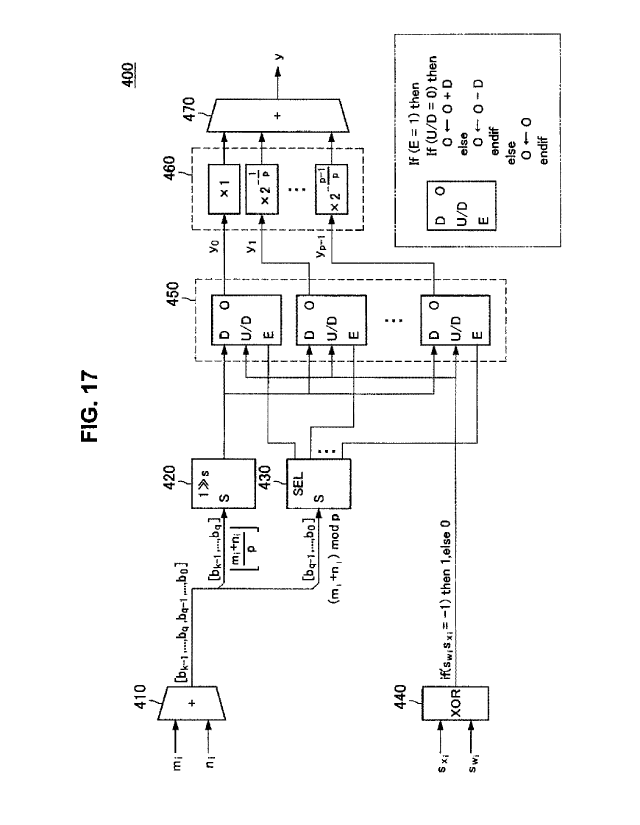
25 The adder-subtractor 360 according to the present embodiment performs
addition and subtraction based on the input s,, the shift operation result,
and the value
of yr. At this point, as described above, the value of yr held in an
accumulator
selected on the basis of the value of the remainder of n, mod p is input into
the adder-
subtractor 360. Also, the yr in the selected accumulator is updated on the
basis of
the computational result by the adder-subtractor 360.
[0088]
CA 03044660 2019-05-22
26
(Multiplier group 370)
The multiplier group 370 according to the present embodiment multiplies yr
updated for each remainder according to the process described above by an
addition
multiplier corresponding to the remainder. For this purpose, the multiplier
group
370 according to the present embodiment includes multiple multipliers
corresponding to each remainder of n, mod p. For example, the multiplier group
370 multiplies yo input from the accumulator group 350 by 1, and multiplies yi
by 2-
up.
[0089]
(Adder 380)
The adder 380 according to the present embodiment adds up the values of yr
calculated for each remainder by the multiplier group 370, and outputs a final
computational result y.
[0090]
The above describes the multiply-accumulate operation circuit 300
according to the present embodiment. As described above, with the multiply-
accumulate operation circuit 300 according to the present embodiment, by
accumulating each yr in accumulators corresponding to each remainder of n, mod
p
and finally performing multiplication collectively, it becomes possible to
minimize
the number of times of multiplications. Note that in the example illustrated
in FIG
16, the calculation is iterated over i to update yr, but it is also possible
to calculate by
performing some or all of the above calculations in parallel.
[0091]
<<2.3. Quantization of both weight vectors and input vectors>>
Next, the technique for the case of quantizing both the weight vectors w and
the input vectors x by a-n/I3 will be described. Herein, a case will be
described in
which a=2, p is an element of the set of natural numbers {1, 2, 3, ...}, and
the inner
product operation is performed. Herein, the input vector component xi and the
weight vector component w, are assumed to be expressed by Formula (20) and
Formula (21) below, respectively. Also, in Formulas (20) and (21) below, it is
assumed that sxi, sw, are elements in the set {-1, 1} and n,, m, are elements
in the set
CA 03044660 2019-05-22
27
{O, 1, 2, ...}.
[0092]
[Math. 12]
= sx 2 P = = = ( 2 0 )
n,
w1= s2 P = = = ( 2 1)
[0093]
Herein, assuming that each of the input vectors x and the weight vectors w
is normalized such that jx,I<1 and Iwil<1, and y is later multiplied by a
normalization
constant as necessary, the inner product operation can be expressed by Formula
(22)
below. Also, herein, yr is defined by Formula (23) below.
[0094]
[Math. 13]
y = sx, 2 P = sw, 2 P
(sx,sõ, )2 P
p-1 {(m,+ni)
= E [E(ss)2 P r((mi+n,)mod p) 2 P = = = (
2 2)
r=0
Yr = E (sx,sw, )2 P r ((m,+n,)mod p) = = = ( 2 3)
[0095]
At this point, if r is an element of the set {0, 1, ..., p-1}, then it becomes
possible to express yr in ordinary fixed-point notation with negative numbers
expressed as two's complement. Note that in the above, p is described as
preferably
being a natural number, but p may also be expressed in an exponential
representation.
For example, in the case of setting p=2q where q is an element of the set {0,
1, 2,
the calculations of int((mi+n,)/p) and (mi+n,) mod p become possible by bit
CA 03044660 2019-05-22
28
truncation making division unnecessary, which has an effect of simplifying the
calculations.
[0096]
At this point, the inner product operation is achievable by the multiply-
accumulate operation circuit 400 illustrated in FIG 17, for example. FIG 17 is
one
example of the multiply-accumulate operation circuit in a case of quantizing
both the
weight vectors and the input vectors according to the present embodiment.
[0097]
Referring to FIG. 17, the multiply-accumulate operation circuit 400
according to the present embodiment is provided with a first adder 410, a
shift
operation unit 420, a selector 430, an XOR circuit 440, an accumulator group
450, a
multiplier group 460, and a second adder 470.
[0098]
(First adder 410)
The first adder 410 according to the present embodiment adds together the
input ml and ni. At this point, as illustrated in the diagram, the result of
adding mi
and ni can be expressed as the bit sequence [bk-I, bq, bq-I, bd.
[0099]
(Shift operation unit 420)
The shift operation unit 420 according to the present embodiment right-
shifts 1 expressed in fixed-point notation by int((mi+n,)/p), on the basis of
the
computation result by the first adder 410. At this time, the value of
int((mckni)/p) is
the value of the most significant bits corresponding to [bk-I, bq] from
the above bit
sequence that is the computational result by the first adder 410. For this
reason, the
shift operation unit 420 preferably performs the shift operation using the
value of the
most significant bits.
[0100]
(Selector 430)
The selector 430 according to the present embodiment selects an adder-
subtractor to execute addition or subtraction from among multiple accumulators
and
adder-subtractors included in the accumulator group 450 on the basis of the
value of
CA 03044660 2019-05-22
29
the remainder of (ml-Fni) mod p, and inputs an Enable signal=1. At this point,
since
the above value of the remainder corresponds to [bg_i, bo]
corresponding to the
least significant q bits from the bit sequence that is the computational
result by the
first adder 410, it is possible to simplify computations similarly to the
above.
[0101]
(XOR circuit 440)
The XOR circuit 440 according to the present embodiment inputs 1 or 0 into
each accumulator of the accumulator group 450 on the basis of the input Sx,
and Sm.
Specifically, the XOR circuit 440 inputs 1 into each accumulator in the case
in which
SS=-1, and 0 in the case in which Sw1Sx,=+1.
[0102]
(Accumulator group 450)
The accumulator group 450 according to the present embodiment is
provided with multiple accumulators corresponding to each value of the
remainder of
(mi-Fni) mod p. Also, the accumulator group 450 includes multiple adder-
subtractors (1-bit up/down counters) corresponding to the accumulators.
[0103]
At this point, as illustrated in the lower-right part of the diagram, each of
the
above adder-subtractors determines whether or not to add or subtract on the
basis of
the Enable signal input from the selector 430. Specifically, only in the case
in
which the input Enable signal is 1, each adder-subtractor adds or subtracts
only 1 bit
with respect to the value 0 held in the corresponding accumulator, in
accordance
with a U/D value input from the XOR circuit 440. With the accumulator group
450
according to the present embodiment, since it is possible to update the values
of yr
with 1-bit addition or subtraction on the most significant bits, an ordinary
adder-
subtractor becomes unnecessary, making it possible to reduce the circuit
scale.
[0104]
(Multiplier group 460)
The multiplier group 460 according to the present embodiment multiplies yr
updated for each remainder according to the process described above by a value
corresponding to the remainder. For this purpose, the multiplier group 460
CA 03044660 2019-05-22
according to the present embodiment includes multiple multipliers
corresponding to
each remainder of (mcFni) mod p. For example, the multiplier group 460
multiplies
yo input from the accumulator group 450 by 1, and multiplies yi by 2-1/P.
[0105]
5 (Second adder 470)
The second adder 470 according to the present embodiment adds up the
values of yr calculated for each remainder by the multiplier group 460, and
outputs a
final computational result y.
[0106]
10 The above
describes the multiply-accumulate operation circuit 400
according to the present embodiment. As described above, with the multiply-
accumulate operation circuit 300 according to the present embodiment, by
accumulating each yr in accumulators corresponding to each remainder of (m-Fn)
mod p and finally performing multiplication collectively, it becomes possible
to
15 minimize the
number of times of multiplications. Note that in the example
illustrated in FIG. 17, the calculation is iterated over i to update yr, but
it is also
possible to calculate by performing some or all of the above calculations in
parallel.
[0107]
Also, in the multiply-accumulate operation circuit 400 illustrated in FIG. 17,
20 an example of
a case of implementing multiple adder-subtractors (1-bit up/down
counters) corresponding to the accumulators in parallel is described, but
instead of
the above configuration, the multiply-accumulate operation circuit 400
according to
the present embodiment may also be provided with a selector and a single adder-
subtractor like in the multiply-accumulate operation circuit 300 illustrated
in FIG. 16.
25 Also,
similarly, it is possible to implement multiple adder-subtractors in parallel
in
the multiply-accumulate operation circuit 300. The configuration of the
multiply-
accumulate operation circuit according to the present embodiment may be
designed
appropriately such that the circuit scale becomes smaller according to the
value of p.
[0108]
30 Also, in the
multiply-accumulate operation circuit 400 illustrated in FIG. 17,
a case of selecting the adder-subtractor and accumulator on the basis of the
least
CA 03044660 2019-05-22
31
significant q bits of (m,+n,) is described. On the other hand, Formula (22)
above is
transformable like Formula (24) below.
[0109]
[Math. 14]
(m,+n,)
y = E(sx,s,õ )2
(mi+n,) mod p __________________________ I
E(si,s,,, )2 2 L P j = = = ( 2 4)
[0110]
For this reason, the inner product operation is also achievable with a single
adder-subtractor, like in the multiply-accumulate operation circuit 500
illustrated in
FIG 18. FIG 18 is one example of the multiply-accumulate operation circuit in
a
case of quantizing both the weight vectors and the input vectors according to
the
present embodiment.
[0111]
Referring to FIG. 18, the multiply-accumulate operation circuit 500
according to the present embodiment is provided with an adder 510, a selector
520, a
memory circuit group 530, a shift operation unit 540, an XOR circuit 550, an
adder-
subtractor 560, and an accumulator 570.
[0112]
(Adder 510)
The adder 510 according to the present embodiment adds together the input
m, and n,. The adder 510 preferably works similarly to the first adder 410
illustrated in FIG. 17.
[0113]
(Selector 520)
The selector 520 according to the present embodiment selects a memory
circuit to connect to the circuit from among multiple memory circuits included
in the
memory circuit group 530, on the basis of the value of [bc,_,, bo]
corresponding to
the least significant q bits.
CA 03044660 2019-05-22
32
[0114]
(Memory circuit group 530)
The memory circuit group 530 according to the present embodiment is
provided with multiple memory circuits corresponding to each value of the
remainder of (m,-Fn,) mod p. In each memory circuit, an addition multiplier
corresponding to each remainder is stored. Note that each memory circuit
provided
in the memory circuit group 530 may be a read-only circuit that holds the
above
addition multiplier as a constant, or may be a rewritable register. The case
of
storing the addition multipliers as constants in read-only circuits has a
merit of
simplifying the circuit configuration while also reducing power consumption.
[0115]
(Shift operation unit 540)
The shift operation unit 540 according to the present embodiment right-
shifts the addition multiplier stored in the connected memory circuit by the
value of
the most significant bits corresponding to [bk-i, bq].
[0116]
(XOR circuit 550)
The XOR circuit 550 according to the present embodiment outputs 1 or 0 on
the basis of the input Sx, and Sw,. The XOR circuit 550 preferably works
similarly
to the XOR circuit 440 illustrated in FIG. 17.
[0117]
(Adder-subtractor 560)
The adder-subtractor 560 according to the present embodiment repeatedly
executes addition or subtraction on y held in the accumulator 570 based on the
computational result by the shift operation unit 540 and the input from the
XOR
circuit 550.
[0118]
(Accumulator 570)
The accumulator 570 according to the present embodiment holds the result y
of the inner product operation.
[0119]
4
CA 03044660 2019-05-22
33
As described above, with the multiply-accumulate operation circuit 500
according to the present embodiment, the inner product operation can be
achieved
with a single adder-subtractor 560 and a single accumulator 570, making it
possible
to reduce the circuit scale further.
.. [0120]
Note that in the above description, a case of using a common p for the input
vectors x and the weight vectors w is described as an example, but in the
information
processing method according to the present embodiment, it is also possible to
use a
different p between the input vectors x and the weight vectors w. In this
case, the
input vectors x and the weight vectors w can be expressed by Formulas (25) and
(26)
below, respectively.
[0121]
[Math. 15]
-- sx, 2 Pm = = = ( 2 5 )
Sly, 2 Pn = = = ( 2 6 )
[0122]
At this point, po is the least common multiple of pm and p,,, or in other
words,
if apm=po and bp,,=po, the input vector component x, and the weight vector
component w, are expressed by Formulas (27) and (28) below, respectively.
[0123]
.. [Math. 16]
_am,
= = = ( 2 7 )
x = sx, 2 P
_bn,
w = sw, 2 Pa = = = ( 2 8 )
[0124]
Consequently, by replacing the operation of m,+n, with am,+bni, and
CA 03044660 2019-05-22
34
additionally replacing p with po, calculation becomes possible similarly to
the above
description, even in the case in which p is different. Also, in the case of
expressing
pn, and pn in an exponential representation, each of am, and bn, can be
computed by
shift operations.
[0125]
Next, the method of quantizing the input vectors x according to the present
embodiment will be described in detail. In the case of quantizing both the
input
vectors x and the weight vectors w, although the quantization of the weight
vectors w
can be calculated in advance, the quantization of the input vectors x must be
performed at runtime. For this reason, a technique of achieving quantization
of the
input vectors x with a small-scale computational circuit is demanded.
[0126]
Here, let jx,j<1 be the bit sequence c=[ck-i, ..., co]. Note that c is a fixed-
point notation in which ck.., corresponds to 1.
[0127]
At this point, let L be the number of bits that are continuously 0 from the
most significant bit (msb) of c. Also, let d be the bit sequence obtained by
left-
shifting c=[ck_i, ..., co] by L bits, and treat this bit sequence in fixed
point notation
with the msb set to 0.5.
[0128]
Next, let rmjn be the minimum r that satisfies Formula (29) below. Note
that herein, r is an element of the set {0, ..., p-1}, but in the case in
which a minimum
r is not found, rnnn=p is set preferably. Here, if In, is defined according to
Formula
(30) below, lx,1 can be approximated, that is, quantized, as Formula (31)
below.
[0129]
[Math. 17]
CA 03044660 2019-05-22
r+1/2
d 2 = = = ( 2 9 )
= = = ( 3 0 )
Ix1
I 2 P = = = ( 3 1)
[0130]
Note that the calculation described above is achievable by providing a
configuration that counts the number of bits that are continuously 0 from the
msb of
5 c as L, and a configuration that compares against a fixed value p times.
[0131]
<<2.4. Effects>>
Next, the effects exhibited by the quantization of the weight vectors w and
the input vectors x according to the present embodiment will be described in
detail.
10 Herein, in the case of quantizing the weight vector component w, and the
input
vector component x, as 2P, the case of p=1, or in other words the case of
using the
quantization technique described in the first embodiment, and the case of p=2,
or in
other words the case of using the quantization technique of the present
embodiment,
were compared.
15 [0132]
Specifically, an experiment was performed in which, after learning the
weight vectors w and the input vectors x by float, the obtained coefficients
are
quantized to the nearest quantization point by each value of p, and compared
to the
image recognition rate in the case of estimating without retraining.
20 [0133]
Note that for the data set, the CIFAR-10 image set (categorized into 10
classes, training data=50000 images, test data=10000 images) was adopted.
[0134]
Also, for the network, an 11-layer ResNet based on ResNet-23 was used.
25 FIG. 19 is a diagram illustrating the network structure of the ResNet
used in the
comparative experiment according to the present embodiment. In FIG 19, the
input
CA 03044660 2019-05-22
36
size input into each layer is indicated on the right side of the diagram,
while each
kernel size is indicated on the left side. Also, as illustrated in FIG 19, the
created
network includes both a ResBlock that does not include a Max Pooling layer and
a
ResBlock that includes a Max Pooling layer. FIGS. 20 and 21 are diagrams
illustrating the network configuration of a ResBlock that does not include a
Max
Pooling layer and a ResBlock that includes a Max Pooling layer, respectively.
[0135]
Next, the technique of quantizing the weight vectors w and the input vectors
x used in the experiment will be described in detail.
[0136]
First, the data in the case of quantizing by p=1 will be described. Herein,
in the quantization of the weight vectors w, 32 values of n from -3 to 12 (16
va1uesx2 ) were used. In this case, the values that the quantized weight
vector
component wi= (2-n) may take are as illustrated in Table 2 below.
.. [0137]
[Table 2]
-3 -2 -1 0 1 2 3 4
2-" 8 4 2 1 0.5 0.25 0.125
0. 0625
5 6 7 8 9 10 11 12
2-" 0.03125 0.015625 0.007813 0.003906
0.001953 0.000977 0.000488 0. 000244
[0138]
Also, in the quantization of the input vectors x, before the input into the
Relu block, three different quantizations with 16 values of n from -4 to 3 (8
va1uesx2 ), 32 values of n from -4 to 11(16 va1uesx2 ), and 64 values of n
from -4
to 27 (32 va1uesx2 ) are performed. In this case, the values that the
quantized input
vector component x,=- (2) may take are as illustrated in Tables 3 to 5 below.
[0139]
[Table 3]
Ii I
CA 03044660 2019-05-22
37
n -4 -3 -2 -1 0 1 2 3
2' 16 8 4 2 1 0.5 0. 25 0.
125
[0140]
[Table 4]
n -4 -3 -2 -1 0 1 2 3
2 " 16 - -8 4 - 2 1 0.5 0.25
0.125
n 4 5 6 7 8 9 10
11
- 2-" 0.0625 0. 03125 0.015625 0.007813
0.003906 0.001953 0.000977 0.000488
[0141]
[Table 5]
n -4 -3 -2 -1 0 1 2 3
2 " 16 8 4 +2 1 1 0.5 0.25 0.125
- -
n 4 5 6 7 8 9 10
11
2-" 0.0625 0.03125 0. 015625 0.007813 0.
003906 0.001953 0. 000977 0.000488
n 12 13 14 15 16 17 18
19
_
2 ' 0.000244 0.000122 6.105-05 3.056-05 1.
53E-05 7. 63E-06 3.815-06 1.915-06
n 20 21 22 23 24 25 26
27
2 " 9. 54E-07 4.775-07 2.385-07 1.195-
07 5.965-06 2.985-08 1. 49E-08 7. 45E-09
[0142]
Next, the data in the case of p=2, or in other words the case of quantizing
using the technique according to the present embodiment will be described.
Herein,
in the quantization of the weight vectors w, 32 values of n from -6 to 9 (16
va1uesx2 ) were used. In this case, the values that the quantized weight
vector
component wi= (2-n/2) may take are as illustrated in Table 6 below.
[0143]
[Table 6]
n -6 -5 -4 -3 -2 -1 o 1
2/2 8 5. 656854 4 2.828427 2
1.414214 1 0.707107
n 2 3 4 5 6 7 8 9
2-"/2 0.5
0.353553 0.25 0.176777 0.125 0.088388 0.0625 0.044194
1
II 1
CA 03044660 2019-05-22
38
[0144]
Also, in the quantization of the input vectors x, before the input into the
Relu block, three different quantizations with 16 values of n from -8 to -1 (8
va1uesx2+), 32 values of n from -8 to 7 (16 va1uesx2+), and 64 values of n
from -8 to
23(32 valuesx2 ) are performed. In this case, the values that the quantized
input
vector component X1= (2-1112) may take are as illustrated in Tables 7 to 9
below.
[0145]
[Table 7]
n -8 -7 -6 -5 -4 -3 -2 -1
22 16
11.31371 8 5.656854 4 2.828427 2 1.414214
[0146]
[Table 8]
n -8 -7 -6 -5 -4 -3 -2 -
1
2-' 16 11.31371 8 5.656854 4
2.828427 2 1.414214
n 0 1 2 3 4 5 6 7
1 0.707107 0.5 0.353553 0.25 0.176777 0.125
0.088388
[0147]
[Table 9]
n -8 -7 -6 -5 -4 -3 -2 -
1
- -2"/2 16 - 11.31371 8 5.656854 4 2.828427 2
1.414214
,
.... - -
n 0 1 2 3 4 5 6 7
2-^/' 1 0.707107 0.5 0.353553 0.25 0.176777
0.125 0.088388
O 8 9 10 11 12 13 14
15
2-"i2 0.0625 0.044194 0.03125 0.022097 0.015625 0.011049 0.007813
0.005524
O 16 17 18 19 20 21 22
23
2" 0.003906 0.002762 0.001953 0.001381 0.000977 0.000691 0.000488
0.000345
[0148]
The comparison results of the image recognition rate in the case of
performing estimation without retraining by the quantization described above
are
1
CA 03044660 2019-05-22
39
illustrated in FIG 22. In FIG. 22, the recognition accuracy is indicated on
the
vertical axis, while the number of quantized values (N values) of the input
vectors x
is indicated on the horizontal axis. Also, in FIG 22, the recognition accuracy
before quantization is indicated by the line segment C, the recognition
accuracy in
the case of quantizing by p=1 is indicated by the line segment P 1 , and the
recognition
accuracy in the case of quantizing by p=2 is indicated by the line segment P2.
[0149]
Herein, a comparison of the line segments P1 and P2 demonstrates that in
the case of 32 or 64 quantized values of the input vectors x, quantizing by
p=2
significantly improves the recognition accuracy over quantizing by p=1. Also,
a
comparison of the line segments P2 and C demonstrates that a large degradation
in
the recognition accuracy is not observed. In other words, this illustrates
how, in the
case in which there is a sufficient number of quantized values of the input
vectors x,
by adopting the quantization technique according to the present embodiment,
even if
retraining is not performed, it is possible to maintain a high recognition
accuracy.
[0150]
In this way, with the quantization method according to the present
embodiment, it becomes possible to effectively reduce the processing load in
inner
product operations while also maintaining high performance of the learning
unit.
[0151]
<<2.5. Example of application to communication technology>>
Next, the application of the quantization technique according to the present
embodiment to other fields will be described. In the above description, the
case of
applying the quantization technique according to the present embodiment to
inner
product operations associated with the forward propagation of a neural network
was
described. On the other hand, the quantization technique according to the
present
embodiment is not limited to the above example, and is also applicable to a
variety of
technologies that perform inner product operations.
[0152]
For example, the quantization technique according to the present
embodiment may also be applied to convolution operations in a bandpass filter
used
CA 03044660 2019-05-22
in the field of communication technology. Hereinafter, a simulation result
when
applying the quantization technique according to the present embodiment to a
bandpass filter will be described.
[0153]
5 FIG 23 is a
diagram illustrating a simulation result according to frequency
characteristics (gain characteristics) when the quantization technique
according to the
present embodiment is applied to a bandpass filter. Herein, the coefficients
(63 tap,
rolloff 0.5) of a root-raised cosine (RRC) filter are quantized.
[0154]
10 Note that in
the quantization, 32 values (0 to 31) are used for each of p=2, 3,
4. In the diagram, this is illustrated as DNN(p,32). Additionally, as a
comparison,
the simulation results in the case of using floating point (Float) and integer
(Linear)
are illustrated as well.
[0155]
15 Herein,
referring to FIG 23, it is demonstrated that even in the case of
applying the quantization technique according to the present embodiment, the
flat
characteristics inside the passband are not degraded. On the other hand,
focusing
on the sidebands demonstrates that even in the case of DNN(2,32), an
attenuation of
approximately -25 dB becomes possible, and furthermore, the attenuation effect
20 becomes
greater with increasing p. Note that the impact of quantization is expected
to be reduced further in combination with a low-pass filter (LPF).
[0156]
Also, FIG. 24 is a diagram illustrating a simulation result according to phase
characteristics when the quantization technique according to the present
embodiment
25 is applied to
a bandpass filter. Referring to FIG 24, it is demonstrated that even in
the case of applying the quantization technique according to the present
embodiment,
phase rotation inside the passband, or in other words degradation of the phase
characteristics, is not confirmed. In this way, the quantization technique
according
to the present embodiment does not greatly degrade the frequency
characteristics of
30 the bandpass
filter, and therefore is also adequately applicable to the field of
communication technology.
CA 03044660 2019-05-22
41
[0157]
In addition, to examine further the impact of the quantization technique
according to the present embodiment, an evaluation according to the bit error
rate
(BER) was performed. FIG 25 is a block diagram utilized in BER evaluation
according to the present embodiment.
[0158]
As illustrated in FIG 25, in this evaluation, floating point, integer, and
DNN(p,32) were applied in an analog-to-digital converter (ADC) and an RRC
filter
before demodulation, and the BER was measured. Also, for the modulation and
demodulation scheme, each of BPSK, QPSK, and 16QAM was used.
[0159]
FIG 26 is a diagram illustrating the BER evaluation result when using
BPSK as the modulation scheme. Also, FIG. 27 is an enlarged view of the data
of
the SNR from 7 to 9 dB in FIG. 26. Referring to FIGS. 26 and 27, it is
.. demonstrated that in the case of using BPSK as the modulation scheme, for
p=4 a
degradation of the BER is not observed at all, and even for p=2 or p=3, the
BER is
not greatly affected.
[0160]
FIG. 28 is a diagram illustrating the BER evaluation result when using
.. QPSK as the modulation scheme. Also, FIG. 29 is an enlarged view of the
data of
the SNR from 10 to 12 dB in FIG. 28. Referring to FIGS. 28 and 29, it is
demonstrated that in the case of using QPSK as the modulation scheme,
similarly to
the case of using BPSK, quantizing according to p=2 or 3 does not greatly
affect the
BER.
[0161]
FIG. 30 is a diagram illustrating the BER evaluation result when using
16QAM as the modulation scheme. Also, FIG 31 is an enlarged view of the data
of
the SNR from 16 to 18 dB in FIG 30. Referring to FIGS. 30 and 31, it is
demonstrated that in the case of using 16QAM as the modulation scheme,
although a
rise in the BER is observed with quantization according to p=2 or 3, a
degradation of
the BER is not confirmed with quantization according to p=4.
CA 03044660 2019-05-22
42
[0162]
As described above, in the case of using BPSK or QPSK for the modulation
scheme, the quantization technique according to the present embodiment is
considered effective regardless of the value of p. Also, in the case of using
16QAM
for the modulation scheme, if p>4, the BER is not considered to be affected.
[0163]
In this way, the quantization technique according to the present embodiment
is also effective in the field of communication technology, and both a
maintaining of
performance and a reduction in processing load may be achieved.
<3. Hardware configuration example>
An example of the hardware configuration common to the information
processing device 10 according to an embodiment of the present disclosure is
now
described. FIG 32 is a block diagram illustrating an example of the hardware
configuration of the information processing device 10 according to an
embodiment
of the present disclosure. Referring to FIG. 32, the information processing
device
10 includes, in one example, a CPU 871, a ROM 872, a RAM 873, a host bus 874,
a
bridge 875, an external bus 876, an interface 877, an input device 878, an
output
device 879, a storage 880, a drive 881, a connection port 882, and a
communication
device 883. Moreover, the hardware configuration shown here is illustrative,
and
some of components can be omitted. In addition, a component other than the
components shown here can be further included.
[0164]
(CPU 871)
The CPU 871 functions as, in one example, an arithmetic processing unit or
a control device, and controls some or all of the operations of each component
on the
basis of various programs recorded in the ROM 872, the RAM 873, the storage
880,
or a removable recording medium 901.
[0165]
(ROM 872 and RAM 873)
The ROM 872 is a means for storing programs loaded into the CPU 871,
data used for operation, or the like. The RAM 873 temporarily or permanently
CA 03044660 2019-05-22
43
stores, in one example, a program to be loaded into the CPU 871, various
parameters
appropriately changing in executing the program, or the like.
[0166]
(Host bus 874, bridge 875, external bus 876, and interface 877)
The CPU 871, the ROM 872, and the RAM 873 are mutually connected via,
in one example, the host bus 874 capable of high-speed data transmission. On
the
other hand, the host bus 874 is connected to the external bus 876 having a
relatively
low data transmission rate, in one example, via the bridge 875. In addition,
the
external bus 876 is connected to various components via the interface 877.
[0167]
(Input device 878)
Examples of the input device 878 include a mouse, a keyboard, a touch
panel, buttons, a switch, a lever, or the like. Furthermore, examples of the
input
device 878 include a remote controller capable of transmitting a control
signal using
infrared rays or other radio waves (hereinafter referred to as a remote
controller). In
addition, the input device 878 includes a speech input device such as a
microphone.
[0168]
(Output device 879)
The output device 879 is a device capable of visually or audibly notifying
the user of the acquired information, which includes a display device such as
a
cathode ray tube (CRT), an LCD, or an organic EL, an audio output device such
as a
loudspeaker or a headphone, a printer, a mobile phone, a facsimile, or the
like. In
addition, the output device 879 according to the present disclosure includes
any of
various types of vibration devices capable of outputting a tactile stimulus.
[0169]
(Storage 880)
The storage 880 is a device used to store various types of data. Examples
of the storage 880 include a magnetic storage device such as hard disk drives
(HDDs), a semiconductor storage device, an optical storage device, a magneto-
optical storage device, or the like.
[0170]
CA 03044660 2019-05-22
44
(Drive 881)
The drive 881 is a device that reads information recorded on the removable
recording medium 901 such as a magnetic disk, an optical disk, a magneto-
optical
disk, or semiconductor memory or writes information to the removable recording
medium 901.
[0171]
(Removable recording medium 901)
Examples of the removable recording medium 901 include a DVD medium,
a Blu-ray (registered trademark) medium, an HD DVD medium, various kinds of
semiconductor storage media, or the like. Of course, the removable recording
medium 901 is preferably, in one example, an IC card or an electronic device
mounted with a contactless IC chip.
[0172]
(Connection port 882)
The connection port 882 is a port used for connection with an external
connection device 902, such as a universal serial bus (USB) port, an IEEE 1394
port,
a small computer system interface (SCSI), an RS-232C port, or an optical audio
terminal.
[0173]
(External connection device 902)
Examples of the external connection device 902 include a printer, a portable
music player, a digital camera, a digital video camera, an IC recorder, or the
like.
[0174]
(Communication device 883)
The communication device 883 is a communication device used for
connection with a network, and examples thereof include a communication card
for
wired or wireless LAN, Bluetooth (registered trademark), or wireless USB
(WUSB),
a router for optical communication, a router for asymmetric digital subscriber
line
(ADSL), or a modem for various communications.
[0175]
<4. Conclusion>
CA 03044660 2019-05-22
As described above, the information processing device according to one
embodiment of the present disclosure is provided with a multiply-accumulate
operation circuit configured to execute a multiply-accumulate operation on the
basis
of multiple input values and multiple weight coefficients that are quantized
by an
5 exponential representation and that correspond to each of the Ogai input
values.
The exponents of the quantized weight coefficients are expressed by fractions
taking
a predetermined divisor p as the denominator. Also, the multiply-accumulate
operation circuit performs the multiply-accumulate operation using different
addition
multipliers on the basis of the remainder determined from the divisor p.
According
10 .. to such a configuration, it becomes possible to further reduce the
processing load
associated with inner product operations while also guaranteeing the
quantization
granularity of the weight coefficients.
[0176]
The preferred embodiment(s) of the present disclosure has/have been
15 described above with reference to the accompanying drawings, whilst the
present
disclosure is not limited to the above examples. A person skilled in the art
can find
various alterations and modifications within the scope of the appended claims,
and it
should be understood that they will naturally come under the technical scope
of the
present disclosure.
20 [0177]
Further, the effects described in this specification are merely illustrative
or
exemplified effects, and are not limitative. That is, with or in the place of
the above
effects, the technology according to the present disclosure can achieve other
effects
that are clear to those skilled in the art from the description of this
specification.
25 [0178]
Additionally, the present technology may also be configured as below.
(1)
An information processing device including:
a multiply-accumulate operation circuit configured to execute a multiply-
30 accumulate operation on the basis of multiple input values and multiple
weight
coefficients that are quantized by an exponential representation and that
correspond
CA 03044660 2019-05-22
46
to each of the input values, in which
exponents of the quantized weight coefficients are expressed by fractions
taking a predetermined divisor as a denominator, and
the multiply-accumulate operation circuit performs the multiply-accumulate
operation using different addition multipliers on the basis of a remainder
determined
from the divisor.
(2)
The information processing device according to (1), in which
the multiply-accumulate operation circuit is provided with multiple different
accumulators configured to hold a computational result for each remainder
determined from the divisor.
(3)
The information processing device according to (2), in which
the remainder is computed by a modulo operation taking a numerator related
to the exponents of the quantized weight coefficients as a dividend, and
the multiply-accumulate operation circuit additionally is provided with a
selector configured to connect the accumulator corresponding to the remainder
to the
circuit.
(4)
The information processing device according to (3), in which
the multiply-accumulate operation circuit additionally is provided with a
shift operation unit that performs a shift operation related to the input
values on the
basis of a value obtained by integerizing a quotient from dividing the
numerator by
the divisor.
(5)
The information processing device according to (1) or (2), in which
the input values are quantized by an exponential representation,
the quantized input values are expressed by fractions taking a predetermined
divisor as a denominator, and
the remainder is remainder from treating a value obtained by summing a
numerator related to the exponents of the quantized weight coefficients and a
CA 03044660 2019-05-22
47
numerator related to the exponents of the quantized input values as a
dividend.
(6)
The information processing device according to (5), in which
the multiply-accumulate operation circuit is provided with multiple adder-
subtractors for each accumulator corresponding to the remainder.
(7)
The information processing device according to (6), in which
the multiply-accumulate operation circuit additionally is provided with a
selector configured to input, on the basis of the remainder, a signal
instructing the
adder-subtractor corresponding to the remainder to execute computation.
(8)
The information processing device according to (1), in which
the multiply-accumulate operation circuit additionally is provided with
multiple memory circuits configured to hold each of the addition multipliers
corresponding to the remainder.
(9)
The information processing apparatus according to (8), in which
the multiply-accumulate operation circuit additionally is provided with a
selector configured to connect the memory circuit corresponding to the
remainder, on
the basis of the remainder.
(10)
The information processing device according to any of (5) to 7, in which
the divisor includes a first divisor determined with respect to the input
values and a second divisor determined with respect to the weight
coefficients, and
the first divisor and the second divisor have mutually different values.
(11)
The information processing device according to any of (1) to 10, in which
the divisor is a natural number.
(12)
The information processing device according to any of (1) to 10, in which
the divisor is expressed by exponentiation.
CA 03044660 2019-05-22
48
(13)
An information processing method including:
executing a multiply-accumulate operation on the basis of multiple input
values and multiple weight coefficients that are quantized by an exponential
representation and that correspond to each of the input values, in which
exponents of the quantized weight coefficients are expressed by fractions
taking a predetermined divisor as a denominator, and
the executing of the multiply-accumulate operation performs the multiply-
accumulate operation using different addition multipliers on the basis of a
remainder
determined from the divisor.
Reference Signs List
[0179]
10 information processing device
110 input unit
120 computation unit
130 storage unit
140 output unit
200, 300, 400, 500 multiply-accumulate operation circuit