Note: Descriptions are shown in the official language in which they were submitted.
85311012
PERMUTATED RING NETWORK
Related Applications
[0001] This application claims priority to U.S. Patent
Application 15/816,374 entitled "Permutated Ring Network",
which was filed on November 17, 2017, and which claims priority
to U.S. Provisional Patent Application 62/425,798, entitled
"Permutated Ring Network".
Field of the Invention
[0002] The present invention relates to a permutated ring
network having a plurality of rings, which provides a scalable,
high-bandwidth, low-latency point-to-point on-chip
communications solution.
RELATED ART
[0003] On-chip communication systems exhibit scaling
problems, and the number of intra-chip communication nodes and
the demand for on chip data bandwidth are ever increasing.
High speed serializing/deserializing (SERDES) communication
protocols are trending toward providing an operating bandwidth
of 100 Gb/sec per pin. Thus, a chip having 1000 pins may
require a chip input/output (I/O) bandwidth of up to 100
Terabit/sec. There is a need to provide on-chip communication
bandwidth to support these specifications. Examples of systems
requiring this bandwidth include a switch fabric for rack scale
data center, neural networks, GPU computing systems, system
level field programmable gate arrays (FPGAs), a many-core
1
Date Recue/Date Received 2022-11-04
CA 03044675 2019-05-22
WO 2018/098087 PCT/US2017/062632
system on a chip (SoC) system, and coherence memory buses for
high-performance multi-core and multi-banked last level caches.
[0004] Physical limitations for on-chip communications
include the length of on-chip wires, which is critical to the
delay and operating frequency. Long wires severely degrade
performance, as the frequency has a first order effect on the
network bandwidth. High fan-out nodes further degrade the
bandwidth by creating place and route congestion, and adding
more gate and wire delays to the network.
[0005] On-chip communication networks are typically
implemented as a synchronous system that operates in response
to a common clock signal. Clock distribution imposes a great
obstacle in building large scale high bandwidth on-chip
networks. More specifically, clock skew will limit the
operating frequency of the network, and the required clock
power may impose limits on the network.
[0006] In addition, challenges exist in typical
communication network topologies, with regard to scaling up the
number of communication nodes and maintaining high operating
frequencies.
[0007] Typical communication network topologies include: 1)
full mesh topology, 2) cross-bar topology and 3) torus network
topology. For each of these network topologies, the delay and
operating frequency of the system will degrade severely as the
wire length of the interconnects increase. Moreover, high fan-
out nodes will cause place and route congestions that will
further degrade the speed and power performance of the system.
[0008] In the full mesh topology, the bandwidth can be
defined by the value N*(N-1)/2, wherein N is the number of
nodes in the network. However, the fan-out of a full mesh
topology system increases as the number of nodes (N) increases.
2
CA 03044675 2019-05-22
WO 2018/098087 PCT/US2017/062632
[ 0009 ] In the cross-bar topology, the number of required
multiplexers increases as the number of nodes (N) in the
network increases, with a scaling factor of N**2. In addition,
the number of inputs per multiplexer increases as the number of
nodes N increases, with a scaling factor of N.
[0010] In the torus network topology, the throughput does
not scale as the number of nodes (N) increases. However, the
fan-out of the nodes undesirably increases as the number of
nodes (N) increase, with a scaling factor of Log(N).
[0011] Because these network topologies are implemented
using on-chip interconnects that are not perfect wires, the
delay and operating frequency of these networks will degrade
severely as wire lengths increase. In addition, high fan-out
nodes will cause place and route congestions that will degrade
the speed and power performance of the networks.
[0012] On one hand, more on-chip bandwidth is needed as
scaling associated with Moore's law and the emergence of new
computing paradigms increase the number of on-chip
communication nodes. However, increasing the number of on-chip
nodes will degrade the system bandwidth due to increases in
wire length and routing congestion when conventional network
topologies are used. Consequently, an on-chip bandwidth
scaling 'wall' effectively limits the growth of on-chip
communication networks.
[0013] It would therefore be desirable to have an improved
network topology capable of overcoming the on-chip bandwidth
scaling wall. It would further be desirable for such a
communications network to be readily scalable, capable of
providing for communication between a thousand or more on-chip
communication nodes. It would further be desirable for such a
communications network to be able to operate at a high
3
85311012
bandwidth, providing upwards of a peta-bit per second of on-chip
communication bandwidth. It would further be desirable for such
a communications network to have a low latency (e.g., below 100
ns latency).
SUMMARY
[0014] Accordingly, the present invention provides a
permutated ring network that includes a plurality of
communication nodes and a plurality of bi-directional
source-synchronous ring networks, each having a plurality of
data transport stations. Each of the communication nodes is
coupled to one of the data transport stations in each of the
plurality of bi-directional source-synchronous ring networks. A
source synchronous technique used to transmit data on the ring
networks mitigates the clock distribution challenges. The number
of bi-directional source-synchronous ring networks can be
selected to provide the bandwidth required by communications
between the various communication nodes. In this manner, the
permutated ring network of the present invention can be readily
scaled.
[0014a] According to one aspect of the present invention, there
is provided a permutated ring network comprising: a plurality of
bi-directional source-synchronous ring networks, each having: a
plurality of data transport stations connected in a ring, a
first message bus for transmitting messages between the data
transport stations in a first direction, a first clock path for
transmitting a first clock signal between the data transport
stations in the first direction, wherein the messages on the
first message bus are latched in the data transport stations in
response to the first clock signal in a source-synchronous
manner, a second message bus for transmitting messages between
the data transport stations in a second direction, opposite the
first direction, and a second clock path for transmitting a
second clock signal between the data transport stations in the
4
Date Recue/Date Received 2022-11-04
85311012
second direction, wherein the messages on the second message bus
are latched in the data transport stations in response to the
second clock signal in a source-synchronous manner; and a
plurality of communication nodes, wherein each of the
communication nodes is coupled to one of the data transport
stations in each of the plurality of bi-directional source
synchronous ring networks, wherein the communication nodes are
coupled to data transport stations having different relative
positions in the plurality of bi-directional source-synchronous
ring networks.
[0014b] According to another aspect of the present invention,
there is provided a permutated ring network comprising: a
plurality of bi-directional source-synchronous ring networks,
each having a plurality of data transport stations connected in
a ring; a plurality of communication nodes, wherein each of the
communication nodes is coupled to one of the data transport
stations in each of the plurality of bi-directional
source-synchronous ring networks; and a routing table that
defines communication paths on the bi-directional
source-synchronous ring networks for communications between each
possible pair of the communication nodes, wherein the routing
table specifies a first group of the possible pairs of the
communication nodes that communicate through paths on the
bi-directional source-synchronous ring networks that include
exactly two of the data transport stations, and a second group
of the possible pairs of the communication nodes that
communicate through paths on the bi-directional
source-synchronous ring networks that include more than two of
the data transport stations.
[0014c] According to still another aspect of the present
invention, there is provided a pelmutated ring network
comprising: a plurality of bi-directional source-synchronous
ring networks, each having a plurality of data transport
stations connected in a ring; a plurality of communication
4a
Date Recue/Date Received 2022-11-04
85311012
nodes, wherein each of the communication nodes is coupled to one
of the data transport stations in each of the plurality of
bi-directional source synchronous ring networks; and a routing
table that defines communication paths on the bi directional
source-synchronous ring networks for communications between each
possible pair of the communication nodes, wherein the routing
table specifies a first group of the possible pairs of the
communication nodes that communicate through paths on a single
one of the bi-directional source synchronous ring networks, and
a second group of the possible pairs of the communication nodes
that communicate through paths on all of the bi-directional
source-synchronous ring networks.
[0014d] According to yet another aspect of the present
invention, there is provided a method of transporting data
between a plurality of communication nodes on an integrated
circuit chip, comprising: transmitting messages from the
communication nodes to a plurality of bi-directional
source-synchronous ring networks, wherein each of the
bi-directional source-synchronous ring networks includes a
plurality of data transport stations connected in a ring, and
each of the communication nodes transmits messages to a data
transport station in each of the bi-directional source-
synchronous ring networks, wherein the communication nodes are
coupled to data transport stations having different relative
positions in the bi-directional source synchronous ring
networks; and transmitting the messages in a source-synchronous
manner between the data transport stations of the bi-directional
source synchronous ring networks.
[0015] The present invention will be more fully understood in
view of the following description and drawings.
BRIEF DESCRIPTION OF THE DRAWINGS
[0016] Fig. 1A is a block diagram of a permutated ring network
that includes eight communication nodes and three bi-directional
4b
Date Recue/Date Received 2022-11-04
85311012
source-synchronous ring networks in accordance with one
embodiment of the present invention.
[0017] Fig. IB is a block diagram illustrating one of the
communication links of the permutated ring network of Fig. lA in
accordance with one embodiment of the present invention.
4c
Date Recue/Date Received 2022-11-04
CA 03044675 2019-05-22
WO 2018/098087 PCT/US2017/062632
[0018] Fig. 10 is a waveform diagram illustrating the source
synchronous timing of various signals of Fig. 18, in accordance
with one embodiment of the present invention.
[0019] Fig. 2 is an interconnect matrix that defines
connections between the communication nodes and data transport
stations of the three ring networks of the permutated ring
network of Fig. lA in accordance with one embodiment of the
present invention.
[0020] Fig. 3 is a routing table that defines the flow of
traffic between the communication nodes through the permutated
ring network of Fig. lA in accordance with one embodiment of
the present invention.
[0021] Fig. 4 is a bandwidth estimation table that defines
the bandwidths between adjacent data transport stations for the
routing table of Fig. 3 in accordance with one embodiment of
the present invention.
[0022] Fig. 5 is a block diagram of a permutated ring
network that includes eight communication nodes and three bi-
directional source-synchronous ring networks in accordance with
an alternate embodiment of the present invention.
[0023] Fig. 6 is an interconnect matrix that defines
connections between the communication nodes and data transport
stations of the three ring networks of the permutated ring
network of Fig. 5 in accordance with one embodiment of the
present invention.
[0024] Fig. 7 is a routing table that defines the flow of
traffic between the communication nodes through the permutated
ring network of Fig. 5 in accordance with one embodiment of the
present invention.
[0025] Fig. 8 is a bandwidth estimation table that defines
the bandwidths between adjacent data transport stations for the
CA 03044675 2019-05-22
WO 2018/098087 PCT/US2017/062632
routing table of Fig. 7 in accordance with one embodiment of
the present invention.
[0026] Fig. 9 is a block diagram of a permutated ring
network that includes eight communication nodes and four bi-
directional source-synchronous ring networks in accordance with
an alternate embodiment of the present invention.
[0027] Fig. 10 is an interconnect matrix that defines
connections between the communication nodes and data transport
stations of the four ring networks of the permutated ring
network of Fig. 9 in accordance with one embodiment of the
present invention.
[0028] Fig. 11 is a routing table that defines the flow of
traffic between the communication nodes through the permutated
ring network of Fig. 9 in accordance with one embodiment of the
present invention.
[0029] Fig. 12 is a block diagram illustrating a
communication node and a corresponding data transport station
in accordance with one embodiment of the present invention.
[0030] Fig. 13 is a block diagram illustrating a
communication node and a corresponding data transport station
in accordance with an alternate embodiment of the present
invention.
DETAILED DESCRIPTION
[0031] In general, the present invention provides a
permutated ring network architecture that includes a plurality
of bi-directional source-synchronous communication rings that
are shared among a plurality of network nodes. A source
synchronous technique is used to mitigate the clock
distribution challenges, wherein a transmitting node sends both
a clock and data to a receiving node. The receiving node
6
CA 03044675 2019-05-22
WO 2018/098087 PCT/US2017/062632
latches the data using the received clock. The clock fan-out
is limited to the size of the data bus width. The clock skew
is set by the delay relationship between the clock and the
corresponding data. Note that the source synchronous technique
will only work with a point-to-point interconnect (e.g., a ring
network). Numerous on-chip interconnect resources are required
to implement a point-to-point network. However, Moore's law
predicts that the number of metal layers will scale upward, the
metal pitch will decrease, and more wires will be available per
unit area as process technologies advance, thereby providing
the on-chip interconnect resources required to implement a
point-to-point network.
[0032] A bi-directional source synchronous ring network
provides a building block for the permutated ring network
architecture of the present invention. A bi-directional ring
network is a simple point-to-point network that provides a fan-
out of 1 (i.e., 1 input and 1 output in each direction for each
node of the network). However, the bi-directional source
synchronous ring network has a fundamental performance
limitation, which is referred to herein as 'hopping loss'.
Hopping loss occurs when a message is required to 'hop' over
nodes located between a transmitting node and a receiving node
on a ring network. As described in more detail below, hopping
loss is minimized or eliminated in the permutated ring network
of the present invention by maximizing the paths available
between adjacent nodes. By using a source synchronous
signaling technique, high-speed, low skew and low power
communication is enabled on the permutated ring network. In
particular embodiments, the permutated ring network of the
present invention enables around a thousand on-chip
communication nodes, and peta-bit per second on-chip
7
CA 03044675 2019-05-22
WO 2018/098087 PCT/US2017/062632
communication bandwidth. The permutated ring network provides
power efficiency and solutions for a wide range of network
sizes, on-chip resource constraints, bandwidth requirements and
application specific optimizations.
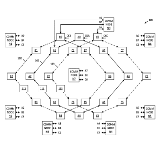
[0033] Fig. 1A is a block diagram of a permutated ring
network 100 in accordance with one embodiment of the present
invention. In the illustrated embodiment, permutated ring
network 100 includes eight communication nodes NO-N7 and three
bi-directional source synchronous ring networks 101, 102 and
103, each of which are fabricated on the same integrated
circuit chip. As described in more detail below, each of the
ring networks 101-103 functions as a communication channel.
Although the illustrated permutated ring network 100 includes
eight communication nodes NO-N7 and three communication
channels 101-103, it is understood that other numbers of
communication nodes and channels can be used in other
embodiments. In general, the number of communication nodes on
the chip is identified by the value, N, and the number of bi-
directional ring networks is identified by the value M. The
number of communication channels (M) is selected to provide an
appropriate tradeoff between the bandwidth requirements of the
communication network and the area-power constraints of the
communication network. The bases for making this selection are
described in more detail below.
[0034] Each of the communication channels 101-103 includes a
plurality of data transport station connected by bi-directional
links (interconnects). More specifically, communication
channel 101 includes data transport stations AO-A7,
communication channel 102 includes data transport stations BO-
B7 and communication channel 103 includes data transport
stations 00-07. The bi-directional links of communication
8
CA 03044675 2019-05-22
WO 2018/098087 PCT/US2017/062632
channel 101 are shown as solid lines that connect the data
transport stations AO-A.7 in a ring. The bi-directional links
of communication channel 102 are shown as dashed lines that
connect the data transport stations BO-B7 in a ring. The bi-
directional links of communication channel 103 are shown as
dashed-dotted lines that connect the data transport stations
C0-C7 in a ring. The bi-directional links allow for the
simultaneous transmission of data/clock signals in both the
clockwise and counterclockwise directions.
[0035] In general, each of the data transport stations AO-
A7, BO-B7 and 00-07 provides an interface that enables the
transfer of data between the communication nodes NO-N7 and the
communication channels 101-103. Details of the structure and
operation of data transport stations AO-A7, BO-B7 and 00-07 and
communication nodes communication nodes NO-N7 are provided in
more detail below.
[0036] In general, each of the communication channels 101-
103 is coupled to receive a master clock signal. Thus, in the
example of Fig. 1A, communication channels 101, 102 and 103 are
coupled to receive master clock signals CKA, CKB and CKC,
respectively. In the embodiment illustrated, data transport
stations AO, BO and CO are coupled to receive the master clock
signals CKA, CKB and CKC, respectively. However, in other
embodiments, other data transport stations in communication
channels 101, 102 and 103 can be coupled to receive the master
clock signals CKA, CKB and CKC, respectively. Although three
separate master clock signals CKA, CKB and CKC are illustrated,
it is understood that each of the master clock signals CKA, CKB
and CKC can be derived from a single master clock signal. In
the described embodiments, each of the master clock signals
CKA, CKB and CKC have the same frequency.
9
CA 03044675 2019-05-22
WO 2018/098087 PCT/US2017/062632
[0037] Conventional clock generation circuitry (e.g., a
phase locked loop circuit) can be used to generate the master
clock signals CKA, CKB and CKC. In the described embodiments,
the master clock signals can have a frequency of about 5 GHz or
more. However, it is understood that the master clock signals
can have other frequencies in other embodiments. The frequency
and voltage of the master clock signals can be scaled based on
the bandwidth demands and power optimization of the ring
network architecture. In the illustrated embodiments, data
transport stations AO, BO and CO receive the master clock
signals CKA, CKB and CKC, respectively. Each of the other data
transport stations receives its clock signal from its adjacent
neighbor. That is, the master clock signals CKA, CKB and CKC
are effectively transmitted to each of the data transport
stations of communication channels 101, 102 and 103,
respectively, in series.
[0038] Each of the communication channels 101, 102 and 103
operates in a source synchronous manner with respect to its
corresponding master clock signal CKA, CKB and CKC,
respectively. Fig. 1B is a block diagram illustrating one of
the communication links between data transport station AO and
data transport station Al in communication channel 101, wherein
this communication link allows for the transmission of a
message MSG A from station logic 120 within data transport node
AO to station logic 130 within data transport node Al in a
source synchronous manner based on the master clock signal CKA.
It is understood that an identical communication link exists to
provide for the transmission of messages from data transport
station Al to data transport station AO in a source synchronous
manner based on the master clock signal CKA (i.e., bi-
directional communication is provided). It is further
CA 03044675 2019-05-22
WO 2018/098087 PCT/US2017/062632
understood that each adjacent pair of data transport stations
in each of the communication channels 101-103 has similar bi-
directional source-synchronous communication links.
[0039] Fig. 13 illustrates relevant portions of data
transport stations AL and Al for the transmission of messages
and clock signals from data transport station AO to data
transport station Al, including station logic 120, delay line
121, multiplexer 122, clock signal line 141, message bus 142
and station logic 130. Fig. 1C is a waveform diagram
illustrating the source synchronous timing of various signals
of Fig. 13, in accordance with one embodiment of the present
invention.
[0040] In general, data transport station AO can transmit
output messages on two paths. In the first path, the message
MSG A received by station logic 120 (e.g., from adjacent data
transport station A7) is forwarded to data transport station
Al. In this case, station logic 130 forwards the message MSG_A
to multiplexer 122. Multiplexer 122 is controlled to route
this message as the output message MSG_AIN. Station logic 120
and multiplexer 122 introduce a delay DAD with respect to the
master clock signal CKA.
[0041] In the second path, a message provided by a
communication node coupled to data transport station AO (e.g.,
communication node Ni) is routed through multiplexer 122.
Multiplexer 122 is controlled to route this message as the
output message MSGAIN. The communication node and the
multiplexer 122 introduce the delay DAD to the message, with
respect to the master clock signal CKA. Fig. 1C illustrates
the delay DAD that exists between the master clock signal CKA
and the transmitted message MSG_AIN.
11
CA 03044675 2019-05-22
WO 2018/098087 PCT/US2017/062632
[0042] Because the transmitted message MSG ()AIN is delayed
with respect to the master clock signal CKA, delay line 121 is
used to add a delay D121 to the master clock signal CKA, thereby
creating the transmitted clock signal CKAIN of data transport
station AO. The delay D121 introduced by delay line 121 is
selected to ensure that the clock signal CKAIN has a proper
setup and hold time with respect to the message MSG AIM
transmitted from data transport station AO. In one embodiment,
the delay D121 of delay line 121 is equalized to the node delay
DA0 described above. That is, the transmitted message MSG AIN is
synchronized to the transmitted clock signal CKAIN using the
known internal delays of the data transport station AO (and the
associated communication node (s)
[0043] Note that the structures 141D and 142D used to
implement the clock signal line 141 and the message bus 142
between data transport stations AO and Al may exhibit
significant delays (e.g., buffer delays). The delays
introduced by clock signal line structure 141D and the message
bus structure 142D are designated as delays D141 and D142,
respectively. Thus, the clock signal CKA
¨OUT received by data
transport station AO is delayed by D:41 with respect to the
clock signal CKAIN transmitted by data transport station AO.
Similarly, the message MSG_AouT received by data transport
station Al is delayed by D142 with respect to the message MSG AIN
transmitted by data transport station AO. This relationship is
shown in Fig. 1C. In order to maintain the desired setup and
hold times established by data transport station AO (when
generating CKAIN and MSG AIN), the delays Drn and D142 must be the
same. It is therefore very important that the wires and
buffers used to implement the clock signal line structure 141D
and the message bus structure 142D are highly equalized and
12
CA 03044675 2019-05-22
WO 2018/098087 PCT/US2017/062632
balanced in order to minimize setup and hold time loss. That
is, the clock path structure 141D and message bus structure
142D should provide substantially identical transmission
characteristics between data transport stations AO and Al, such
that the relative phases of the transmitted clock signal CKAIN
and the transmitted message MSG_AIN are maintained at the
receiving data transport station Al by received clock signal
CKAouT and received message MSG_Aourr-
[0044] In accordance with the above-described example, the
clock path 141 and the message bus 142 operate as a wave
pipeline system, wherein messages transmitted on the message
bus 142 are latched into the receiving node in a source-
synchronous manner using the clock signal transmitted on the
clock path 141. In this manner, messages are transmitted from
data transport station AO to data transport station Al at the
frequency of the master clock signal CKA, allowing for fast
data transfer from data transport station AO to data transport
station Al. During normal operation, the station logic within
each of the data transport stations AO-A7, BO-B7 and C0-C7
latches incoming messages in response to a corresponding
received clock signal.
[0045] Because point-to-point source-synchronous
communication is implemented, the wire and buffer delays D141
and D142 of the clock signal line structure 141D and the message
bus structure 142D will not degrade the operating frequency of
the communication channels 101-103. In accordance with one
embodiment, the frequencies of the master clock signals CKA,
CKB and CKC are higher than the frequencies of the local clock
signals used to operate the communication nodes NO-N7.
[0046] Because the station logic of the data transport
stations have a relatively simple design, the transmission of
13
CA 03044675 2019-05-22
WO 2018/098087 PCT/US2017/062632
messages on the permutated ring network can be performed at a
relatively high frequency. Communication nodes NO-N7 typically
includes a more complicated design, and may operate at a slower
frequency than the frequency of the master clock signals CKA,
CKB and CKC. That is, while communication nodes NO-N7 may
receive messages from the permutated ring network at the
frequency of the master clock signals CKA, CKB and CKC, the
communication nodes NO-N7 are not required to respond at the
frequency of the master clock signals CKA, CKB and CKC.
[0047] Note that the circular configuration of the
communication channels 101-103 necessitates that messages
received by data transport stations AO, BO and CO (e.g., the
data transport stations that receive the master clock signals
CKA, CKB and CKC) must be resynchronized to the master clock
signals CKA, CKB and CKC, respectively. For example, a message
transmitted from data transport station A.7 to data transport
station AO is synchronized to a delayed version of the master
clock signal CKA within data transport station A7. As a
result, clock domain crossing synchronization is necessary
within the data transport station AO (i.e., the message
received from data transport station A7 must be resynchronized
with the master clock signal CKA within data transport station
AO). In one embodiment, resynchronization circuitry (not
shown) performs this synchronizing operation by latching the
incoming message into a first flip-flop in response to the
incoming clock signal received from data transport station A7.
The message provided at the output of this first flip-flop is
then latched into a second flip flop in response to the master
clock signal CKA. The second flip-flop provides the
synchronized message MSG_A, which is provided to station logic
14
CA 03044675 2019-05-22
WO 2018/098087 PCT/US2017/062632
120. This synchronized message MSG A is stored in station
logic 120 in response to the master clock signal CKA.
[0048] Returning now to the topography of the permutated
ring network 100, each of the communication nodes NO-N7 is
coupled to a unique one of the data transport stations AO-A7,
BO-B7 and CO-C7 in each of the three communication channels
101-103. For example, communication node NO is connected to
data transport station Al in communication channel 101, data
transport station BO in communication channel 102 and data
transport station CO in communication channel 103. Table 1
below defines the connections between each of the communica-
tion nodes NO-N7 and the data transport stations AO-A7, BO-B7
and CO-C7 in accordance with the described embodiment. Note
that the physical connections between the communication nodes
N1-N7 and the data transport stations AO-A7, BO-B7 and CO-C7
are not explicitly shown in Fig. 1A for clarity.
TABLE 1
DATA TRANSPORT DATA TRANSPORT DATA TRANSPORT
COMMUNICATION STATION IN COMM STATION IN COMM STATION IN COMM
NODE CHANNEL 101 CHANNEL 102 CHANNEL 103
NO Al BO CO
Ni AO B4 C3
N2 A2 B6 C5
N3 A3 B3 Cl
N4 AA B1 C4
N5 A5 B5 C7
N6 A6 B7 C2
N7 A7 B2 C6
[0049] Fig. 2 re-orders the data of Table 1 to provide an
interconnect matrix 200 of the three communication channels
101-103, wherein the interconnect matrix 200 is ordered by the
CA 03044675 2019-05-22
WO 2018/098087 PCT/US2017/062632
data transport stations in each of the communication channels
101-103. This interconnect matrix 200 makes it easy to
determine the number of hops between the communication nodes
NO-N7 on each of the communication channels 101-103. Note that
the communication nodes NO-N7 are coupled to data transport
stations having different relative positions in the three
communication channels 101-103. As described in more detail
below, this configuration allows for the versatile and
efficient routing of messages between the communication nodes.
[0050] Fig. 3 is a routing table 300, which defines the flow
of traffic among the communication nodes NO-N7 through the
permutated ring network 100 in accordance with the present
embodiment. For example, communication nodes NO and Ni
communicate using the path between data transport stations AO
and Al on communication channel 101. The number of hops along
this path is defined by the number of segments traversed on the
communication channel 101. Because data transport stations AO
and Al are adjacent to one another on communication channel 101
(i.e., one segment exists between data transport stations AO
and Al), the communication path between nodes NO and N1
consists of one hop (1H).
[0051] As illustrated by routing table 300, most of the
communication paths between nodes NO-N7 include unique one hop
communication paths. However, because there are 24 unique
communication segments provided by the three communication
channels 101-103, and 28 unique communication node pairs, the
permutated ring network 100 is unable to provide unique one hop
communication paths between each of the communication node
pairs. Thus, routing table 300 provides two-hop (2H)
communication paths for four of the communication node pairs
(i.e., node pair NO and N7; node pair N1 and N2; node pair N3
16
CA 03044675 2019-05-22
WO 2018/098087 PCT/US2017/062632
and N5; node pair N4 and N6). For example, nodes NO and N7
communicate using three different two hop paths, including a
first path between data transport stations A7, AO and Al on
communication channel 101, a second path between data transport
stations BO, B1 and B2 on communication channel 102, and a
third path between data transport stations C6, C7 and CO on
communication channel 103.
[0052] The communication among the data transport stations
AO-A7, BO-B7 and CO-C7 will operate at the highest frequency
allowed by the source synchronous network. This frequency is
not reduced as the number of communication nodes and the number
of communication channels scale up. It is understood that each
of the communication channels 101-103 includes provisions for
initialization, arbitration, flow control and error handling.
In one embodiment, these provisions can be provided using well
established techniques.
[0053] Fig. 4 is a bandwidth estimation table 400, which
defines the bandwidths between adjacent data transport stations
for routing table 300 of permutated ring network 100. Thus,
based on routing table 300, the link between data transport
stations AO and Al may be used to transmit data between
communication nodes NO and N1, between communication nodes NO
and N7, and between communication nodes N1 and N2.
[0054] In the described example, four pairs of communication
nodes communicate using three 2-hop paths. More specifically,
communication nodes NO and N7 communicate using three 2-hop
paths A7-AO-A1, C6-C7-00 and BO-B1-B2; communication nodes Ni
and N2 communicate using three 2-hop paths AO-A1-A2, C3-C4-05
and B4-B5-B6; communication nodes N3 and N5 communicate using
three 2-hop paths A3-A4-A5, C7-CO-C1 and B3-B4-B5; and
communication nodes N4 and N6 communicate using three 2-hop
17
CA 03044675 2019-05-22
WO 2018/098087 PCT/US2017/062632
paths A4-A5-A6, 02-03-04 and B7-BO-B1. In the described
example, the pairs of communication nodes using three 2-hop
paths are considered to be lower capacity pairs, which do not
require as much bandwidth as other pairs of communication
nodes. In the present example, the bandwidth allotted to
communications between each of the pairs of communication nodes
using three 2-hop paths is (arbitrarily) limited to 60 percent
of the bandwidth available of a link between adjacent data
transport stations (e.g., the bandwidth allotted to
communications between nodes NO and N7 is limited to 60% of the
bandwidth provided by the link between data transport stations
AO and Al).
[0055] Using communication nodes NO and N7 as an example,
there are three 2-Hop paths between nodes NO and N7 (i.e., A7-
AO-Al, 06-07-00 and BO-B1-B2). If the allotted bandwidth is
divided equally among these three 2-hop paths, then this
allotted bandwidth accounts for 20% (60%/3) of the available
bandwidth on each of the associated links.
[0056] Taking all 12 of the above-described 2-hop paths into
account, the bandwidth allotted to communication between nodes
NO-N7, N1-N2, N3-N5 and N4-N6 accounts for 20% of the bandwidth
on the links between the following data transport stations: Ad-
A2, A3-A4, A5-A6, AO-A7, Bl-B2, B3-B4, B5-B6, BO-B7, CO-C1, C2-
C3, C4-05 and C6-C7. This leaves 80% of the bandwidth of these
links available for the communication nodes coupled by 1-hop
paths provided by these links. For example, 80 percent of the
bandwidth of the link between data transport stations Al and A2
is allocated to the 1-hop connection between communication
nodes NO and N2, while 20 percent of the bandwidth of the link
between data transport stations Al and A2 is allocated to a 2-
hop connection between communication nodes N1 and N2.
18
CA 03044675 2019-05-22
WO 2018/098087 PCT/US2017/062632
[0057] Similarly, taking all 12 of the above-described 2-hop
paths into account, the bandwidth allotted to communication
between nodes NO-N7, N1-N2, N3-N5 and N4-N6 accounts for 40% of
the bandwidth on the links between the following data transport
stations: AO-Al, A4-A5, BO-B1, B4-B5, 03-C4 and CO-C7. This
leaves 60% of the bandwidth of these links available for the
communication nodes coupled by 1-hop paths provided by these
links. For example, 60 percent of the bandwidth of the link
between data transport stations AO and Al is allocated to the
1-hop connection between communication nodes NO and Ni, while
20 percent of the bandwidth of the link between data transport
stations AO and Al is allocated to a 2-hop connection between
communication nodes NO and N7, and 20 percent of the bandwidth
of the link between data transport stations AO and Al is
allocated to a 2-hop connection between communication nodes N1
and N2.
[0058] Note that some of the links between data transport
stations are not used in any of the twelve 2-Hop paths. In
these instances, 100% of the bandwidth of links that are not
used in the 2-hop paths is available to connect the associated
communication nodes. In the present example, 100% of the
bandwidth of the links between data transport stations A2-A3,
A6-A7, B2-B3, B6-B7, Cl-C2 and C5-C6 is available to provide 1-
hop communication between communication node pairs N2-N3, N6-
N7, N3-N7, N2-N6, N3-N6 and N2-N7, respectively.
[0059] Note that Table 400 shows the 1-Hop bandwidth
available between adjacent data transport stations, in
accordance with the description provided above. The total 1-
Hop bandwidth of each of the communication channels 101-103 is
6.6 in the example of Figs. 1-4, which is a more than 3x
improvement over a simple bi-directional ring network (which
19
CA 03044675 2019-05-22
WO 2018/098087 PCT/US2017/062632
has a corresponding 1-Hop bandwidth of 2). Hence, the use of
three communication channels in the permutated ring network 100
results in a 3.3x bandwidth improvement over three simple bi-
directional ring networks. Note that the bandwidth improvement
becomes more significant as the number of communication
channels increases.
[0060] In the example of Figs. 1-4, the 1-Hop bandwidth
between each pair of communication nodes is not equal. Thus,
the placement of various communication nodes in the permutated
ring network should be selected to match the communication
needs of the various communication nodes. In the example of
Figs. 1-4, it is desirable to locate pairs of communication
nodes having higher bandwidth requirements at node locations
N2-N3, N6-N7, N3-N7, N2-N6, N3-N6 and N2-N7. Thus, the
communication patterns of the communication nodes is an
important consideration for the design of the permutated ring
network 100. Stated another way, the communication patterns of
the nodes are an important consideration for the optimization
of the interconnect matrix 300.
[0061] As described above, some of the communication paths
of permutated ring network 100 require 2-hops, which results in
the fundamental above-described performance limitations, which
is referred to herein as 'hopping loss'. As described above,
permutated ring network 100 provides 24 pairs of 1-hop links,
and 28 possible unique connections between the communication
nodes NO-N7. Because a unique 1-Hop connection cannot be
provided for each possible pair of communication nodes, hopping
loss exists (because some connections must be multi-hop
connections). In order to maximize the total 1-Hop bandwidth,
the interconnect matrix 200 and the routing table 300 are
optimized with the following constraints: 1) maximize the
CA 03044675 2019-05-22
WO 2018/098087 PCT/US2017/062632
number of unique single hop connections, and 2) for the
remaining multi-hip connection pairs, maximize the path
diversity and minimize the number of hops in each hopping path.
[0062] The interconnect matrix 200 and the routing table 300
are determined by the network size and the application specific
bandwidth requirements of the communication nodes NO-N7. For
example, in networks with limited area or power budgets, the
number of channels provisioned will most unlikely be sufficient
to completely eliminate the 'hopping loss', so the interconnect
matrix and the routing table are designed to maximize the total
bandwidths among all the communication nodes. If the network
requires that a subset of the communication node pairs must
have zero hopping loss in order to avoid significant
performance degradation, then the interconnect matrix is
designed to satisfy this constraint. Given enough
communication channels, a non-blocking, fault-tolerant
communication with broadcast ability can be constructed.
Various manners of implementing such designs are described in
more detail below.
[0063] A specific example of the manner in which a
permutated ring network can be designed for use with a
particular set of communication nodes is described in more
detail below in connection with Figs. 5-8.
[0064] Fig. 5 is a block diagram illustrating a permutated
ring network 500 that includes eight communication nodes CPU 0,
CPU 1, CPU 2, CPU 3, MB 0, MB 1, MB 2 and MB 3, which are
_ _ _ _ _ _ _
connected by communication channels 101-103, including data
transport stations AO-A7, BO-B7 and 00-07. Communication
channels 101-103 and data transport stations AO-A7, BO-B7 and
CO-C7 have been described above. Each of the communication
nodes CPU 0, CPUml, CPU_2 and CPU_3 is an on-chip processor,
21
CA 03044675 2019-05-22
WO 2018/098087 PCT/US2017/062632
and each of the communication nodes MB 0, MB 1, MB 2 and MB _3
is an on-chip memory bank, wherein each of the processors
CPU 0, CPU 1, CPU 2 and CPU 3 is able to access each of the
_ _ _ _
memory banks MB 0, MB 1, MB 2 and MB 3, as well as each of the
other processors (e.g., processor CPU_O can access each of
processors CPU 1, CPU2 and CPU 3)
[0065] Fig. 6 is an interconnect matrix 600 that specifies
the connections between the communication nodes CPU 0, CPU_l,
CPU_2, CPU_3, MB_O, MB_1, MB__2 and MB__3 and the data transport
stations AO-A7, BO-B7 and 00-07. Fig. 7 is a routing table 700
that specifies the data transport stations used to link the
various pairs of communication nodes, as well as the number of
hops include in each link. Fig. 8 is a bandwidth estimation
table 800, which defines the bandwidths between adjacent data
transport stations for routing table 700 of permutated ring
network 500.
[0066] Interconnect matrix 600 and routing table 700 are
selected based on the specific requirements of communication
nodes CPU 0, CPU_1, CPU_2, CPU 3, MB_O, MB_1, MB__2 and MB3 and
the data transport stations AO-A7, BO-B7 and 00-07.
[0067] Communication channels 102 and 103 (including data
transport stations BO-B7 and 00-07) are used for communications
between processors CPU 0, CPU_1, CPU_2 and CPU3 and memory
banks MB 0, MB 1, MB _2 and MB 3. More specifically, each of
the processors CPU 0, CPU_1, CPU_2 and CPU___3 has a unique 1-Hop
connection to each of the memory banks MB_O, MB_1, MB__2 and
MB 3, using communication channels 102 and 103. The full
bandwidth of a 1-Hop link is therefore available for
communications between the processors CPU 0, CPU_1, CPU2 and
CPU 3 and the memory banks MB_O, MB_1, MB 2 and MB 3 (see,
_ _ _
bandwidth estimation table 800). There are no communication
22
CA 03044675 2019-05-22
WO 2018/098087 PCT/US2017/062632
links among the memory banks MB 0, MB 1, MB 2 and MB 3 (as it
is not necessary for the memory banks MB_O, MB_1, MB2 and MB__3
to communicate with one another in the described example).
[0068] Communication channel 101 (including data transport
stations AO-A7) is used for communications between processors
CPU 0, CPU_1, CPU2 and CPU_3, as well as other memory
interconnect functions, including arbitration, synchronization,
cache snooping, broadcasting and multicasting. As illustrated
by Fig. 8, the available bandwidth between the processors
CPU 0-CPU 3 is less than the available bandwidth between the
processors CPU_O-CPU_3 and the memory banks MB_O-MB_3.
However, in the described example, communications between
processors CPU 0, CPU 1, CPU 2 and CPU 3 can tolerate the
hopping losses that exist on communication channel 101.
[0069] Another specific example of the manner in which a
permutated ring network can be designed for use with a
particular set of communication nodes is described in more
detail below in connection with Figs. 9-11. Fig. 9 is a block
diagram illustrating a permutated ring network 900 that
includes eight communication nodes NO-N7, which are connected
by four communication channels 101-104, including data
transport stations AO-A7, BO-B7, CO-C7 and DO-D7.
Communication channels 101-103 and data transport stations AO-
A7, BO-B7 and CO-C7 have been described above, and the
additional communication channel 104 and data transport
stations DO-D7 are similar. The addition of communication
channel 104 increases the total number of available 1-Hop links
to 32, such that each of the 28 possible links between the
communication nodes NO-N7 can be implemented using a 1-hop
link. As a result, hopping loss can be completely eliminated
in permutated ring network 900 (i.e., each communication node
23
CA 03044675 2019-05-22
WO 2018/098087 PCT/US2017/062632
can communicate with each other communication node directly),
thereby creating a fully non-blocking network. In the
described embodiment, the permutated ring network is fabricated
on a single integrated circuit chip.
[0070] Fig. 10 is an interconnect matrix 1000 that specifies
the connections between the communication nodes NO-N7 and the
data transport stations AO-A7, BO-B7, CO-C7 and DO-D7. Fig. 11
is a routing table 1100 that specifies the data transport
stations used to link the various pairs of communication nodes,
as well as the number of hops included in each link. Note that
each of these links has an estimated bandwidth of 1.0 (i.e.,
100% of the available bandwidth between adjacent data transport
stations).
[0071] In the embodiment of Figs. 9-11, there are four pairs
of connections between each of the communication nodes NO-N7
and the communication channels 101-104. The bandwidth of the
permutated ring network 900 may be limited by this
configuration. That is, the peak bandwidth of the permutated
ring network 900 may be limited by the interconnects between
the communication nodes NO-N7 and the communication channels
101-104. Thus, although the peak bandwidth of the permutated
ring network 900 is capable of supporting the bandwidth demand
of all nodes NO-N7 communicating among each other
simultaneously, there may not be not enough bandwidth to
transport the messages from the communication nodes NO-N7 to
the communication channels 101-104. In this instance, the
communication channels 101-104 will have extra (unused)
bandwidth. This extra bandwidth has several advantages,
including: 1) less congestion at the communication nodes (e.g.,
four pairs of wires at each communication node, versus seven
pairs of wires, which would otherwise be required to allow a
24
CA 03044675 2019-05-22
WO 2018/098087 PCT/US2017/062632
communication node to simultaneously communicate with the seven
other communication nodes), 2) each pair of communication nodes
can communicate via other channels, such that the permutated
ring network 900 provides path diversity (and therefore
provides fault tolerance) (That is, because the permutated ring
network 900 has excessive bandwidth, each source communication
node can optionally use channels other than its assigned
channel to communicate to a target communication node. Of
course, this will incur some unnecessary hopping loss.
However, the extra bandwidth of the permutated ring network 900
can absorb some limited amount of hopping loss), and 3) the
communication channels 101-104 of permutated ring network 900
can provide other important communication functions (e.g.,
broadcasting and multicasting) using the extra bandwidth of the
permutated ring network 900.
[0072] As described above, each of the data transport
stations transfers data between a communication node and a
corresponding communication channel (or forwards data between
adjacent data transport stations on the corresponding
communication channel). Operation of the data transport
stations, communication nodes and communication channels will
now be described in more detail, using a particular example
that includes data transport station Al, communication node NO
and communication channel 101. It is understood that the other
data transport stations operate in a manner similar to data
transport station Al (and that the other communication nodes
operate in a manner similar to communication node NO).
[0073] Fig. 12 is a simplified block diagram illustrating
communication node NO and data transport station Al in
accordance with one embodiment of the present invention.
CA 03044675 2019-05-22
WO 2018/098087 PCT/US2017/062632
[0074] Data transport station Al includes station logic
1201, multiplexer 1202, receive FIFO 1203, transmit FIFO 1204
and delay line 1205, which are dedicated to the propagation of
clockwise messages (e.g., M1 IN and M1 OUT) and a clockwise
clock signal (e.g., CK1 IN and CKl_OUT) on communication
channel 101. Data transport station Al further includes
station logic 1211, multiplexer 1212, receive FIFO 1213,
transmit FIFO 1214 and delay line 1215, which are dedicated to
the propagation of counter-clockwise messages (e.g., M2IN and
M2 OUT) and a counter-clockwise clock signal (e.g., CK2 IN and
CK2 OUT) on communication channel 101. Arbitration logic 1210,
delay line 1220 and multiplexer 1225 are used to account for
conflicts between simultaneous messages received in the
clockwise and counter-clockwise directions, and transmit
messages/clock signal to communication node NO.
[0075] Communication node NO includes communication node
logic 1230, receive FIFO 1231, transmit FIFO 1232, delay line
1234, communication node clock generator 1235 and synchronizer
circuit 1236. In general, communication node clock generator
1235 generates a local clock signal OK NO, which is used to
control most operations within communication node NO. For
example, communication node logic 1230 controls the operations
of communication node NO, including the reading of messages
from receive FIFO 1231 and the writing of messages to transmit
FIFO 1232, in response to the local clock signal CK_NO.
[0076] The 'clockwise' data transport circuitry will now be
described in more detail. Note that the 'counter-clockwise'
data transport circuitry operates in a similar manner.
[0077] There are two sets of source-synchronized
interconnect buses associated with data transport station Al.
In the clockwise direction, an incoming message Ml_IN and
26
CA 03044675 2019-05-22
WO 2018/098087 PCT/US2017/062632
source-synchronous clock signal CK1 IN are received from
adjacent data transport station A2, and an outgoing message
M1 OUT and source synchronous clock signal CK1 OUT are
transmitted to adjacent data transport station AO. In the
counter-clockwise direction, an incoming message M2_IN and
source-synchronous clock signal 0K2 IN are received from
adjacent data transport station AO, and an outgoing message
M2 OUT and source synchronous clock signal CK2 OUT are
transmitted to adjacent data transport station A2. Both of
these clock signals CK1 IN and CK2 IN are derived from the
master clock signal CKA of the corresponding communication
channel 101.
[0078] When the message M1 IN arrives at data transport
station Al, it is latched by station logic circuitry 1201 in
response to the source clock signal CKl_IN. Station logic 1201
determines whether the received message Ml_IN targets
(addresses) the data transport station Al. If so, station
logic 1201 writes the received message M1 IN to receive FIFO
1203 (e.g., by activating a corresponding write enable signal
WE1). In a similar manner, station logic 1211 writes counter-
clockwise messages M2 IN that target data transport station Al
to receive FIFO 1213 (e.g., by activating a corresponding write
enable signal WE2). Station logic circuits 1201 and 1211
inform arbitration circuit 1210 when messages are stored in
receive FIFOs 1203 and 1213. In response, arbitration circuit
1210 controls read operations from receive FIFOs 1203 and 1213,
and controls multiplexer 1225 to route either message M1 IN or
M2 IN as message MIN to the receive FIFO 1231 of communication
node NO. The read operations implemented by arbitration
circuit 1210 are performed in response to an arbitrarily
selected one of the source clock signals CK1 IN or CK2mIN. In
27
CA 03044675 2019-05-22
WO 2018/098087 PCT/US2017/062632
the illustrated example, arbitration circuit 1210 performs read
operations from receive FIFOs 1203 and 1213 using the source
clock signal CKl_IN. Arbitration circuit 1210 controls the
read out of these messages M1 IN and M2 IN using a conventional
arbitration policy, which specifies that as long as a message
is present in either FIFO 1203 or 1213, a message will always
be read out by arbitration circuit 1210. In this manner,
messages stored in the receive FIFOs 1203 and 1213 are sent to
communication node NO serially using a pre-defined arbitration
policy.
[0079] Arbitration circuit 1210 also controls multiplexer
1225 to route the source clock signal used to read messages
from the receive FIFOs 1203 and 1213 (e.g., source clock signal
CK1 IN in the present example) to delay line 1220, which delays
_
the received clock signal to create the input clock signal
OK IN. The delay introduced by delay line 1220 is selected to
maximize the set up and hold times with respect to the message
M IN.
[0080] The message MIN is written in a source synchronous
manner, wherein the message MIN is latched into the receive
FIFO 1231 in response to the input clock signal OK IN. The
message MIN is subsequently read out of the receive FIFO 1231
to the control node logic 1230 in response to the local clock
signal OK NO.
[0081] If the received message M1 IN does not target data
transport station Al (i.e., the message 'hops' over data
transport station Al), then station logic 1201 controls
multiplexer 1202 to route the received message to data
transport station AO as the output message Ml_OUT. Delay line
1205 introduces a delay to the source clock signal CK1 IN to
generate the output clock signal 0K1 OUT, which is also routed
28
CA 03044675 2019-05-22
WO 2018/098087 PCT/US2017/062632
to data transport station AO. The delay line 1205 introduces a
delay selected such that the message Ml_OUT has an appropriate
set up and hold time with respect to the output clock signal
CK1 OUT (in the manner described above in connection with Figs.
1B and 1C).
[0082] Communication node NO may also generate messages to
transmit to data transport station Al. In one embodiment,
communication node logic 1230 generates a message M_NO, which
is written to transmit FIFO 1232 in the clock domain of the
local clock signal CM NO. This message M NO is read from the
transmit FIFO 1232 in the clock domain of the input clock
signal CK_IN. Note that arbitration circuit 1210 always causes
multiplexer 1225 to route the selected source clock signal
CK1 IN to generate the input clock signal CM IN, even if there
_ _
are no messages Ml_IN or M2_IN being received. The messages
M_ NO read from transmit FIFO 1232 are provided to transmit
FIFOs 1204 and 1214 in data transport station Al.
Communication node logic 1230 provides write enable signals W3
and W4 to synchronizer circuit 1236, which synchronizes these
write enable signals W3 and W4 with the input clock signal
CM IN, thereby creating synchronized write enable signals WE3
and WE4, respectively. These write enable signals WE3 and WE4
are provided to transmit FIFOs 1204 and 1214, respectively,
wherein the write enable signals WE3 and WE4 allow
communication node NO to write the message M_NO to the desired
one of transmit FIFOs 1204 or 1214. The message M_NO is
written to the selected transmit FIFO 1204 or 1214 in a source
synchronous manner using an output clock signal CK_OUT, which
is a delayed version of the input clock signal CK_IN used to
read the message M_NO from the transmit FIFO 1232. In the
illustrated example, delay line 1234 introduces an appropriate
29
CA 03044675 2019-05-22
WO 2018/098087
PCT/US2017/062632
delay to the input clock signal OK _IN to generate the output
clock signal OK OUT, such that the set up and hold times with
respect to the messages M_NO read from transmit FIFO 1232 are
maximized.
[0083]
Assume that the message M NO is stored in transmit
FIFO 1204. In this case, station logic 1201 activates a read
enable signal RE1, which causes the message M NO to be read out
to multiplexer 1202. Station logic 1202 controls multiplexer
1202 to route this message M_NO on the communication channel
101 as the output message M1 OUT. Note that station logic 1201
ensures that this output message Ml_OUT has the proper phase
relationship with the corresponding output clock signal
CK1 OUT. That is, the output message M1 OUT is routed such
that the set up and hold times of this message are maximized
with respect to the output clock signal CKl_OUT.
[0084]
Station logic 1211 operates in a similar manner to
read messages from transmit FIFO 1214 (using read enable signal
RE2), and route these messages through multiplexer 1212 as the
output message M2 OUT.
[0085] The
embodiment of Fig. 12 advantageously minimizes
the number of clock generators required to implement the
permutated ring network of the present invention.
[0086] Fig.
13 is a simplified block diagram illustrating
communication node NO and data transport station Al in
accordance with an alternate embodiment of the present
invention. Similar elements in Figs. 12 and 13 are labeled
with similar reference numbers. Thus, the data transport
station Al of Fig. 13 includes station logic 1201, multiplexer
1202, receive FIFO 1203, transmit FIFO 1204 and delay line
1205, which are dedicated to the propagation of clockwise
messages, and station logic 1211, multiplexer 1212, receive
CA 03044675 2019-05-22
WO 2018/098087 PCT/US2017/062632
FIFO 1213, transmit FIFO 1214 and delay line 1215, which are
dedicated to the propagation of counter-clockwise messages.
Communication node NO includes communication node logic 1230,
receive FIFO 1231, transmit FIFO 1232 and communication node
clock generator 1235 and synchronization circuit 1236, which
have been described above in connection with Fig. 12.
[0087] In general, the communication node NO of Fig. 13
includes a communication node to data transport station (CN-
DTS) clock generation circuit 1301 that generates a local clock
signal OK CD, which is used to control the transfer of data
between the communication node NO and the data transport
station Al. (This contrasts with the embodiment of Fig. 12,
which use the clock signals CK1 IN and 0K2 IN from the
communication channel 101 to control the transfer of data
between the communication node NO and the data transport
station Al.)
[0088] Thus, in the embodiment of Fig. 13, the CK_CD signal
is used to read the message M NO from the transmit FIFO 1232 of
communication node NO to the transmit FIFOs 1204 and 1214 in
data transport station Al. Delay line 1302 introduces a delay
to the CK CD clock signal, thereby generating a delayed output
clock signal CK_OUT, which is provided to transmit FIFOs 1204
and 1214 in data transport station Al. The delay introduced by
delay line 1302 is selected to maximize set up and hold time
with respect to the message M_NO. Synchronization circuit 1236
synchronizes write enable signals W3 and W4 provided by
communication node logic 1230 with the clock signal OK CD,
thereby providing write enable signals WE3 and WE4,
respectively, which are provided to transmit FIFOs 1204 and
1214, respectively of the data transport station Al. The
messages M_NO are latched into transmit FIFOs 1204 and 1214 in
31
CA 03044675 2019-05-22
WO 2018/098087 PCT/US2017/062632
a source synchronous manner in response to the write enable
signals WE3 and WE4, respectively, and the output clock signal
CK OUT. Although the OK_ CD clock signal is not needed by
_
transmit FIFOs 1204 and 1214 if there are no messages M NO
being transmitted, this CK_CD clock signal is continuously
transmitted to the data transport station Al, because the data
transport station Al uses this OK _CD clock signal for source
synchronous transfer of messages from the data transport
station Al to the communication node NO (as described in more
detail below).
[0089] The messages Ml_IN and M2_IN received from the
communication channel 101, and stored in receive FIFOs 1203 and
1213 of data transport station Al, are read out to multiplexer
1225 by arbitration circuit 1310. Arbitration circuit 1310
controls the read out of these messages Ml_IN and M2IN using a
conventional arbitration policy, which specifies that as long
as a message is present in either FIFO 1203 or 1213, a message
will always be read out by arbitration circuit 1310.
[0090] Arbitration circuit 1310 controls multiplexer 1225 to
selectively route the retrieved messages Ml_IN and M2IN to the
receive FIFO 1231 of communication node NO as the input message
MIN. In the embodiment of Fig. 13, arbitration circuit 1310
_
receives (and operates in the domain of) the CK_CD clock signal
provided by communication node NO. Thus, messages are read out
of receive FIFOs 1203 and 1213 in response to the CK_CD clock
signal. Delay line 1303 within data transport station Al
introduces a delay to the CK CD clock signal, thereby providing
the input clock signal OK IN, which is used to transfer the
messages MIN provided by multiplexer 1225 into the receive
FIFO 1231 of communication node NO in a source synchronous
manner. The delay introduced by delay line 1303 is selected to
32
CA 03044675 2019-05-22
WO 2018/098087 PCT/US2017/062632
maximize the set-up and hold time of this source synchronous
transfer.
[0091] In accordance with one embodiment of the present
invention, the frequency of the OK _CD clock signal is selected
to optimize the bandwidth requirement between communication
node NO and data transport station Al. The CK_CD clock signal
can have a frequency other than the frequency communication
node domain clock signal CK_NO and the frequency of the clock
signals CKl_IN and 0K2 IN of the communication channel 101.
Moreover, the frequency of the OK _CD clock signal can be
different within each of the communication nodes NO-N7. For
example, in the embodiment described above in connection with
Figs. 1-4, which implements 8 communication nodes NO-N7 and
three communication channels 101-103, communication nodes N4
and N5 can only communicate via data transport stations A4-A5
at 60% of the full bandwidth. In this example, the frequency
of the OK _CD clock signal can be set to 60% of the frequency of
the communication channel (e.g., 60% of CK1 IN or CK2 IN), and
still provide the required data transfer capacity.
[0092] In the embodiment of Figs. 9-11, which implements 8
communication nodes NO-N7 and four communication channels 101-
104, the extra bandwidth of the permutated ring network 800 can
be utilized by setting the frequency of the CK_CD clock signals
in each of the communication nodes NO-N7 to a frequency faster
than the frequency of the communication channels 101-104. In
this manner, the embodiment of Fig. 13 provides great
flexibility for optimizing the operating frequencies of the
permutated ring network.
[0093] The permutated ring network architecture of the
present invention can be scaled in both the number of
communication nodes (N) and the number of communication
33
CA 03044675 2019-05-22
WO 2018/098087 PCT/US2017/062632
channels (M). The operating frequency of the data transport
stations will not be slowed down by scaling the permutated ring
network architecture. In addition, scaling up the number of
communication channels M will provide a highly non-linear
improvement on the total bandwidth of the permutated ring
network architecture.
[0094] The permutated ring network architecture of the
present invention can be used to implement high bandwidth
switch chips, provide an interconnect for a many-core system on
a chip, provide an interconnect for graphics processor unit
(GPU) chips, provide an interconnect for a system level FPGA,
or implement coherence memory buses for high-performance multi-
core and multi-banked last level cache memories.
[0095] Although the invention has been described in
connection with several embodiments, it is understood that this
invention is not limited to the embodiments disclosed, but is
capable of various modifications, which would be apparent to a
person skilled in the art. Accordingly, the present invention
is limited only by the following claims.
34