Note: Descriptions are shown in the official language in which they were submitted.
VOLTAGE CONVERTER SYSTEMS
Field
[0002] The present invention relates generally to voltage converter
systems, in
particular to systems adapted to convert direct-current (DC) voltages to
alternating-current (AC)
voltages and vice versa.
Background
[0003] A DC-AC voltage converter is an electrical system that changes
a DC voltage
to an AC voltage. The converted AC voltage may have any desired voltage level,
waveform and
frequency with the use of appropriate transformers, switching, filtering and
control circuits. DC-
AC voltage converters are used in a wide range of applications, from small
switching power
supplies in electronic devices such as computers to large electric utility
high-voltage direct
current applications that transport bulk power. DC-AC voltage converters are
also commonly
used to supply AC power from DC sources such as solar panels or batteries.
[0004] Fig. 1 shows a typical prior art DC-AC voltage converter 10,
which operates at
a relatively low frequency. Voltage converter 10 is relatively simple, but it
suffers from
significant disadvantages. A first disadvantage is cost, because it uses a low-
frequency
transformer 12 that requires a relatively large amount of copper for
transformer windings. In
recent years the cost of copper has increased, while the cost of power
semiconductors has
decreased. This trend is expected to continue. In addition, a low-frequency
transformer has
relatively low efficiency when it is configured with a relatively high winding
turns ratio and is
used for voltage step-up. An example of such configurations is a DC-AC voltage
converter with
1
CA 3045199 2019-06-04
a step-up transformer having a turns ratio of about 19:1 or more and a
relatively low input
voltage power source, for example about 10 to 20 volts DC.
Summary
100051 Given the foregoing, it is desirable to perform voltage
conversion with a
relatively high-frequency transformer driven by suitable power switching
semiconductors. In one
embodiment the present invention is a DC-AC voltage converter capable of
operating with a
relatively low DC voltage source input, such as from a battery power supply.
100061 In some embodiments of the present invention the DC-AC
voltage converter
may be bidirectional, thereby capable of receiving an AC voltage signal and
generating an output
DC voltage signal. This arrangement is useful, for example, for charging a
battery from an AC
arid.
(0007] Preferably, a transformer is utilized to provide electrical
isolation for DC-AC
and AC-DC conversion. For example, an isolation transformer may be used
between a DC
voltage input (e.g., a battery) and an AC voltage output. The voltage
converters of the present
invention may be generally divided into several types according to the type of
transformer
selected. For example, the isolation transformers may be relatively low-
frequency, on the order
of 50/60 Hertz (Hz). Preferably, the isolation transformers are relatively
high-frequency, on the
order of tens or more kilohertz (kHz).
100081 An aspect of the present invention is a voltage converter
system that includes a
first, high-frequency, DC-AC voltage converter configured to receive a first
DC voltage signal
and generate a first AC voltage signal. A DC link is configured to receive the
first AC voltage
signal and convert the first AC voltage signal to a second DC voltage signal.
A second DC-AC
2
CA 3045199 2019-06-04
voltage converter is configured to receive the second DC voltage signal and
generate a second
AC voltage signal.
[0009] Another aspect of the present invention is a voltage
converter system that
includes a DC-AC voltage converter configured to receive a DC voltage signal
and generate a
first, relatively high-frequency, AC voltage signal. An AC-AC voltage
converter is configured to
receive the first AC voltage signal and generate a second AC voltage signal.
The frequency of
the second AC voltage signal is preferably lower than the frequency of the
first AC voltage
signal.
[0010] Yet another aspect of the present invention is a voltage
converter system that
includes a first voltage converter portion that is configured to receive a DC
voltage signal and
convert the DC voltage signal to pulses of DC voltage. A second voltage
converter portion is
configured to receive the pulses of DC voltage and convert the pulses of DC
voltage to a
relatively low-frequency AC voltage signal. The voltage converter system is
selectably
configurable as a DC-AC voltage converter or an AC-DC voltage converter. In
some
embodiments of the present invention the first voltage converter portion
includes a tuk-type
voltage converter and a single-ended primary inductor converter (SEP1C)
voltage converter, the
Cuk-type voltage converter and the SEPIC voltage converter being electrically
combined to
operate cooperatively.
Brief Description of the Drawings
100111 Further features of the inventive embodiments will become
apparent to those
skilled in the art to which the embodiments relate from rcading the
specification and claims with
reference to the accompanying drawings, in which:
3
CA 3045199 2019-06-04
[0012] Fig. 1 is an electrical schematic diagram of a typical prior
art DC-AC voltage
converter;
[0013] Fig. 2 is an electrical schematic diagram of a DC-AC voltage
converter system
with a DC link according to an embodiment of the present invention;
100141 Fig. 3 is an electrical schematic diagram of a DC-AC voltage
converter system
without a DC link according to another embodiment of the present invention;
[0015] Fig. 4 is an electrical schematic diagram of a voltage
converter configurable
for operation as either a DC-AC or an AC-DC voltage converter according to yet
another
embodiment of the present invention;
100161 Fig. 5 is an electrical schematic diagram showing details of
a first portion of
the voltage converter of Fig. 4;
100171 Fig. 6 is a graph showing the general waveform of certain
electrical signals
generated by the circuit of Fig. 5;
100181 Fig. 7 is an electrical schematic diagram showing details of
a second portion
of the voltage converter of Fig. 4;
[0019] Fig. 8 is an electrical schematic diagram of a Cuk-type
voltage converter;
[00201 Fig. 9 is an electrical schematic diagram of a single-ended
primary inductor
converter voltage converter;
100211 fig. 10 is an electrical schematic diagram of the voltage
converters of Figs. 8
and 9 electrically combined together in a new arrangement in accordance with
an embodiment of
the present invention, providing for a reduced total component count;
[0022] Fig. 11 is an electrical schematic diagram of the voltage
converter of Fig. 10
incorporating several refinements; and
4
CA 3045199 2019-06-04
[0023] Fig. 12 is an electrical schematic diagram of a voltage
converter according to
yet another embodiment of the present invention.
Detailed Description
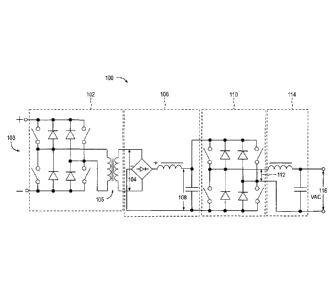
100241 Fig. 2 shows a DC-AC voltage converter system 100 having a
first, high-
frequency. DC-AC voltage converter 102 according to an embodiment of the
present invention.
First DC-AC voltage converter 102 receives at an input 103 a first DC voltage
signal. A first,
relatively high-frequency, AC voltage signal 104 generated by a transformer
105 of first DC-AC
voltage converter 102 is supplied to a DC-link 106 that converts the first AC
voltage signal to a
second DC voltage signal 108. Second DC voltage signal 108 is coupled to a
second DC-AC
voltage converter 110 that converts second DC voltage signal 108 to a second
AC voltage signal,
output AC voltage signal 112, Output 112 may have either low-frequency
components, high-
frequency components, or both low- and high-frequency components.
[0025] An optional electrical filter 114 provides filtering of AC
output voltage signal
112 to remove high-frequency components and/or limit electromagnetic
interference (EMI)
caused by the AC output voltage signal, resulting in a filtered AC output
voltage signal 116. For
certain applications where power quality is not a significant issue (such as a
motor drive, as one
example) a filter 114 configured to remove high-frequency components may be
omitted.
f00261 Fig. 3 shows a DC-AC voltage converter system 200 according
to another
embodiment of the present invention. A first AC voltage signal 202 generated
by a DC-AC
voltage converter 204 is supplied to an AC-AC voltage converter 206 that
converts the first AC
voltage signal to a second AC voltage signal, output AC voltage signal 208. An
electrical filter
210 provides filtering of AC output voltage signal 208 to reduce EMI caused by
the AC output
voltage signal, resulting in a filtered AC output voltage signal 211. First AC
voltage signal 202
CA 3045199 2019-06-04
is a relatively high-frequency voltage signal, while second AC voltage signal
208 is a relatively
low-frequency voltage signal output from voltage converter system 200.
[0027] With reference to Figs. 2 and 3 together, voltage converter
system 100
provides relatively efficient voltage conversion, but compared to voltage
converter system 200 it
is more complex and more expensive to produce. However, the performance of
voltage
converter system 200 depends in part upon the operating conditions of a
transformer 212. Fig. 3
shows a topology wherein transformer 212 operates under regulation, with a
relatively high turns
ratio. In this case efficiency of voltage converter system 200 will be less
and the voltage
converter system will generate a relatively high level of EMI on the AC output
voltage signal
208. Consequently, EMI filter 210 may require a number of relatively expensive
components in
order to be effective.
100281 Fig. 4 shows a schematic diagram of a voltage converter
system 300 according
to yet another embodiment of the present invention. Voltage converter system
300 is
configurable for operation as either a DC-AC or an AC-DC voltage converter and
is suitable for
low DC input voltages (e.g., on the order of about 8-16 VDC) at power levels
of up to several
kilowatts. Furthermore, voltage converter system 300 overcomes the
disadvantages discussed
above. Voltage converter system 300 may be implemented with a relatively low
number of
active semiconductor switches. In addition, a transformer 302 (comprising
windings 302A,
302B) functions under extremely benign conditions (i.e., conditions favorable
in that root-mean-
square (RMS) current and RMS voltage are favorable for relatively low
transformer losses).
Finally, there is only a low level of EMI on the AC side.
100291 The topology of voltage converter system 300 may be divided
into two
portions for the purpose of explanation. A first voltage converter portion,
400 shown in Fig. 5,
6
CA 3045199 2019-06-04
provides pulses of DC voltage regulated from 0 volts to a predetermined
maximum voltage, with
a generally half-sinusoidal waveform as shown in Fig. 6. A second voltage
converter portion
500, shown in Fig. 7, provides electrical isolation and conversion from the
pulsed DC voltage of
Fig. 6 to a predetermined relatively low-frequency AC voltage signal
including, without
limitation, about 120 VAC at a frequency of about 50/60 Hz.
100301 With continued reference to Fig. 5, this power stage is a
combination of two
types of power converters. The first is a uk-type voltage converter 600, shown
in Fig. 8. The
other is a single-ended primary inductor converter (SEPIC) voltage converter
700, shown in Fig.
9. The operational details of these voltage converters are well-known in the
art and thus will not
be further elaborated upon here. Both voltage converters have a number of
common features.
For example, each is capable of providing an output voltage from zero to
several times higher
than the input voltage. In addition, both are bi-directional.
[0031] One important difference between the t uk-type voltage
converter and the
SEPIC-type voltage converter is that the uk-type voltage converter reverses
the polarity of the
input voltage while the SEPIC-type voltage converter does not. With reference
again to Fig. 5,
these characteristics may be utilized to advantage, to provide an output
voltage from an
appropriately paired and electrically combined uk-type voltage converter and
SEPIC-type
voltage converter that is about twice the output voltage available from each
voltage converter
individually, each voltage converter providing about half of output power
delivered by the
electrically combined voltage converters. A further advantage of this
arrangement is that
doubling the output voltage in this manner aids to reduce the required primary-
to-secondary
winding turns ratio of isolation transformer 302.
7
CA 3045199 2019-06-04
[0032] With reference now to Figs. 8 and 9 together, switches 602,
702 respectively
exhibit substantially the same operating characteristics. Likewise, inductors
604, 704 in Figs. 8
and 9 respectively exhibit substantially the same operating characteristics.
Therefore, these
components can be combined in an appropriately paired euk-type voltage
converter and SEPIC-
type voltage converter to form the circuit 800 shown in Fig. 10. In Fig. 10,
switch 802 replaces
switches 602, 702 while inductor 804 replaces the inductors 604, 704. Thus,
switch 802 and
inductor 804 are common to both the uk-type voltage converter and the SEPIC
voltage
converter. This results in one less active switch and one less inductor in an
appropriately paired
Cuk-type voltage converter and SEPIC-type voltage converter, thereby reducing
voltage
converter cost. Circuit 800 may be substituted for circuit 400 in the system
of Fig. 4.
[00331 euk and SEPle voltage converters have one common
disadvantage in that
neither provide forward power conversion. Rather, they use passive components
such as
capacitors and inductors for energy storage. Consequently, the efficiency of
these voltage
converters depends very much on the quality factor of the aforementioned
passive components.
The quality factor of capacitors are generally good, but the quality factor of
inductors are often
less than desirable and often tend to worsen under high-current and low-
voltage operating
conditions. To reduce losses and increase efficiency, system 800 may be
modified, replacing
inductor 804 with an inductor/ transformer 904, as shown in the circuit 900 of
Fig. 11. In this
embodiment of the present invention when a switch 902 begins conducting
forward power
conversion will be provided by inductor/transformer 904, thereby increasing
the efficiency of
system 900 in comparison to system 800 of Fig. 10. Circuit 900 may be
substituted for circuit
400 in the system of Fig. 4.
8
CA 3045199 2019-06-04
[0034] With reference again to Fig. 7, voltage converter portion 500
comprises a
power stage which will provide isolation between the low voltage side and the
high voltage side.
This topology is a series-resonant voltage converter, which is bi-directional.
The power
transformer 302 in this case works under substantially benign conditions, with
a generally
trapezoidal voltage wave form and a generally sinusoidal current wave form.
The transformer
302 leakage inductance is part of the resonant inductor or, optionally, may
comprise the entire
resonant inductor. All these features aid to keep efficiency and the
commutation frequency as
high as possible. This reduces the transformer size and reduces its cost, as
well as total inverter
cost, reducing the cost of EMI filters if used.
[0035] A voltage converter 1000 is shown in Fig. 12 according to yet
another
embodiment of the present invention. Like voltage converters 800 and 900,
voltage converter
1000 may be substituted for circuit 400 in the system of Fig. 4.
[0036] Voltage converter 1000 includes a first inductor 1002 and a
second inductor
1004 connected in series, the first and second inductors each having an input
and an output. A
first capacitor 1006 is electrically intermediate the first and second
inductors 1002, 1004, a first
terminal of the first capacitor being electrically connected to the output of
the first inductor and a
second terminal of the first capacitor being electrically connected to the
input of the second
inductor. A third inductor 1008 and a fourth inductor 1010 are connected in
series, the third and
fourth inductors each having an input and an output. A second capacitor 1012
is electrically
intermediate the third and fourth inductors 1008, 1010, a first terminal of
the second capacitor
being electrically connected to the output of the third inductor and a second
terminal of the
second capacitor being electrically connected to the input of the fourth
inductor. A first switch
1014 is coupled between the input of the first inductor 1002 and the output of
the third inductor
9
CA 3045199 2019-06-04
1008. A second switch 1016 is coupled between the output of the first inductor
1002 and the
input of the third inductor 1008. A rectifier 1018 is arranged such that an
anode of the rectifier is
electrically connected to the second terminal of the first capacitor 1006, a
cathode of the rectifier
being electrically coupled to the second terminal of the second capacitor
1012. A third switch
1020 is electrically connected in parallel with the rectifier 1018. Voltage
converter 1000 is
configured to receive a DC voltage signal at the inputs of the first and third
inductors 1002, 1008
and to generate an AC voltage signal at the outputs of the second and fourth
inductors 1004,
I 0.
[0037] Voltage converter system 1000 may further include third
capacitor 1022, the
third capacitor being electrically intermediate the second and fourth
inductors 1004, 1010. A
first terminal of third capacitor 1022 is electrically connected to the output
of the second inductor
1004 and a second terminal of the third capacitor is electrically connected to
the output of the
fourth inductor 1010.
[0038] The foregoing configuration of voltage converter system 1000
has the
advantage of relatively low inductor current and a low switch current, similar
to the embodiment
of Fig 5. since there are two input inductors (1002 and 1008) rather than the
single input inductor
of the previously-described configurations, and also has a low number of
switches similar to the
embodiment of Fig. 10. It should be noted that voltage converter system 1000
has more input
current ripple compared to the embodiment of Fig. 5. as half of the input
current is discontinuous
because it flows through the switches, it is important in this embodiment that
the switches switch
synchronously to eliminate voltage transients across the switches and losses.
[0039] Inductors 1002, 1008 of voltage converter system 1000 may
optionally be
coupled magnetically to allow current balancing to occur. The current in
inductor 1008 and
CA 3045199 2019-06-04
switch 1014, and in inductor 1002 and switch 1016, may not necessarily ramp up
identically as
these inductor-switch pairs are independent of one another. However, when
switches 1014, 1016
are opened the current flows in a complete circuit through the output (i.e.,
"a" and "b" of Fig. 12)
so the current in inductors 1002, 1008 must be substantially the same. Any
error will result in
the energy being dumped in the switches 1014, 1016 until the currents are
substantially the same.
If the windings 1002, 1008 are coupled the energy can transfer between the
windings until the
currents are substantially the same rather than the energy being lost.
100401 In some embodiments of the present invention certain
inductors of voltage
converter system 1000 may be wound upon a common core. For example, inductors
1002, 1008
may be wound upon a common core. Similarly, inductors 1004, 1010 may be wound
upon a
common core. Winding the inductors upon a common core may provide certain
advantages, such
as a reduction in the overall size of the inductors.
100411 One skilled in the art will appreciate that any suitable
electronic components
may be utilized for the circuits shown in the accompanying figures and
described herein. For
example, the switches may be any suitable types of power switching components
including,
without limitation, semiconductors such as bipolar junction transistors, field
effect transistors and
thyristors. Likewise, the diodes, capacitors, inductors and transformers shown
in the
accompanying figures may be any suitable types and values for a particular
realization of the
circuitry.
[0042] In addition, the circuits shown in the accompanying figures
are simplified for
purposes of explanation and are not intended to be limiting in any way.
Accordingly, the circuits
may include any suitable number and type of ancillary components including,
without limitation,
11
CA 3045199 2019-06-04
biasing, feedback and filtering components and circuitry as well as analog
and/or digital
monitoring, feedback and control circuitry.
10043] While
this invention has been shown and described with respect to a detailed
embodiment thereof, it will be understood by those skilled in the art that
changes in form and
detail thereof may be made without departing from the scope of the claims of
the invention.
12
CA 3045199 2019-06-04