Note: Descriptions are shown in the official language in which they were submitted.
CA 03045918 2019-05-10
WO 2018/156374
PCT/US2018/017895
NITRIDE STRUCTURE HAVING GOLD-FREE CONTACT AND METHODS
FOR FORMING SUCH STRUCTURES
TECHNICAL FIELD
[0001] This disclosure relates generally to a structure having a gold-free
electrical contact
structure in contact with an upper surface of a Nitride.
BACKGROUND
[0002] As is known in the art, many monolithic microwave integrated circuits
(MMICs)
having Group III-Nitride semiconductors, sometimes referred to as nitride
semiconductors, such as for example, gallium nitride-based (AlGaN/GaN) high
electron
mobility transistors (HEMTs), are increasingly being used for high-frequency
and high-
power applications. Group III-Nitride are herein after sometimes also referred
to as Group
III-N which includes, for example, binaries InN, GaN, AIN, their ternary
alloys such as
(AlGaN) alloys and other nitrogen based alloys.
[0003] In order to realize the potential of these HEMT devices it is necessary
to achieve
low-resistance, good edge acuity and reliable metal to metal contacts, and
metal to
semiconductor Ohmic contacts. Most Group III-N foundry metal to metal and
metal to
semiconductor low resistance Ohmic contacts use gold (Au) to reduce sheet
resistance (for
transmission lines and Ohmic contacts) and to decrease oxidation during the
high
temperature anneal required to achieve the lowest metal to semiconductor Ohmic
contact
resistance to active devices.
[0004] As is also known, in many Monolithic Microwave Integrated Circuits
(MMICs)
and other integrated circuits (ICs), electrical connection is made to the
bottom of the
MMIC for both ground and electrical signals to mounted chips, these
connections are
made through electrically conductive vias passing through the substrate and/or
a
semiconductor epitaxial layer on at least a portion of the substrate to
electrical contacts
that connect the vias to a metallization on the wafer; sometimes referred to
as a front-side
metallization.
1
CA 03045918 2019-05-10
WO 2018/156374
PCT/US2018/017895
[0005] Traditionally, Group III-N HEMT MMICs and devices are fabricated by
liftoff-
based processing in III-V foundries. Recently, however, Group III-N HEMTs have
begun
to be fabricated using high yield silicon (Si) like, Au-free, subtractive
processing
techniques in Si CMOS foundry environments. More particularly, a "lift-off'
process is
where a mask has a window to expose a selected portion of a surface where a
material is to
be deposited. The material is deposited onto the mask with a portion of the
material
passing through the window onto the exposed selected portion of the surface.
The mask is
lifted off the surface with a solvent along with portion of the material on
the mask (the
unwanted portion of the deposited material) while leaving the desired portion
of the
material on the exposed selected portion of the surface. A "subtractive"
process is where a
material is first deposited over the entire surface. Then a mask is formed to
cover only
over a selected portion of the deposited material (the portion which is to
remain after the
processing); the unwanted portions of the deposited material being exposed. An
etchant is
then brought into contact with the mask thereby removing the exposed unwanted
portion
while the mask prevents the etchant from removing the covered desired portion
of the
material.
[006] Relative to Si CMOS foundries, it is well known that the yield and cost
of III-V
compound semiconductor devices and circuits (processed in traditional III-V
foundries) has
long been limited by low wafer volumes, increased substrate handling during
processing,
the widespread use of liftoff-based processing techniques to define metal
lines, and the use
of time consuming electron beam lithography for sub 500 nm gate lithography.
The Si
CMOS foundry environment on the other hand has the benefit of high wafer
volumes, large
wafer diameters (>200 mm), highly automated cassette to cassette wafer
fabrication or
processing tools, subtractive processing techniques, advanced optical
lithography cluster
tools and techniques (capable of defining sub 100 nm features), and the
Moore's law
paradigm that drives both equipment development and technology node
development.
[0007] However, as noted previously, to take advantage of the benefits of the
Si foundry
infrastructure and background Si CMOS wafer volumes, the developed Group III-N
processes have to be Au-free. Gold is a deep level trap dopant in Si.
Therefore, Au is not
allowed in the front end or back end of Si CMOS foundry fabrication lines as
it is a
serious contamination concern that can cause catastrophic yield problems.
2
CA 03045918 2019-05-10
WO 2018/156374
PCT/US2018/017895
[0008] Gold free processing of GaN (or other III-V) device wafers in Si
foundry
environments therefore requires the use of Si foundry back end of line (BEOL)
compatible
metallizations such as aluminum (Al) or copper (Cu). Copper is the most
attractive of
these metals to use as it has superior electrical conductivity and electro-
migration
resistance. However, because of the lack of volatile copper dry etch
byproducts, copper
cannot readily be subtractively patterned by the techniques of
photolithography wherein
photoresist masking and plasma etching have been used with great success with
aluminum. To process copper, the Damascene process (which is also
subtractive), was
developed. In the Cu Damascene process, a host insulator material for the
copper,
typically an underlying insulating layer (usually silicon dioxide), is
patterned with open
trenches where the copper is to be formed. A thick coating of copper that
significantly
overfills the trenches is deposited on the insulating layer, and chemical-
mechanical
planarization (CMP) is used to remove the excess copper that extends above the
top of the
insulating layer. Cu filled within the trenches of the insulating layer is not
removed and
becomes the patterned conductive interconnect.
[0009] As is also known in the art, while Cu is manageable, it also poses its
own
contamination risk for Si foundries. Barrier layers should completely surround
all copper
interconnections, since diffusion of copper into surrounding materials would
degrade their
properties. Typically, the trenches are lined with thin tantalum (Ta) and /or
tantalum
nitride (TaN) metal layers (as part of the Ta/TaN/Cu plating seed metal stack)
to act as
diffusion barriers along the bottom and sides of the Cu metal interconnects.
At post Cu
CMP the top of the interconnect metal is coated with SiNx to act as the top
interface
diffusion barrier, to prevent oxidation during interlayer oxide deposition,
and to act as a
stop etch layer (during the trench etch of the silicon dioxide) for additional
interconnect
formation. Additional process complications arise, however, when back to front
side
metal interconnects are facilitated by through-wafer or through-semiconductor
layer vias
that require a chlorine-(or other oxidizer) based etches to form these vias.
The chloride-
based etch by-products are nonvolatile and the etch process results in a
degraded Cu
interfacial surface.
3
CA 03045918 2019-05-10
WO 2018/156374
PCT/US2018/017895
SUMMARY
[0010] In accordance with the disclosure, a semiconductor structure is
provided having: a
substrate; a Group III-N semiconductor layer disposed on the substrate; and a
multi-layer,
electrical contact structure in contact with the Group III-N semiconductor
layer. The
electrical contact structure comprises: a gold-free contact layer in contact
with the Group
III-N semiconductor layer; and a gold-free electrically conductive etch stop
layer
electrically connected to the gold-free contact layer. An electrically
conductive via passing
through the substrate to the etch stop layer.
[0011] In one embodiment, the multi-layer, electrical contact structure
comprises an
aluminum-based layer disposed over the gold-free contact layer.
[0012] In one embodiment, the gold-free contact layer is in direct contact
with the Group
III-N semiconductor layer and wherein the gold-free contact layer and the
aluminum-
based layer have physical annealing properties enabling annealing with the
Group III-N
semiconductor layer at a temperature less than 660 degrees to form an Ohmic
contact with
the Group III-N semiconductor layer.
[0013] In one embodiment, an electrode contact is electrically connected to
the multi-layer
electrical contact structure and the multi-layer, electrical contact structure
and the
electrode contact provide a source, drain or gate electrode structure.
[0014] In one embodiment the electrode contact is a gold-free electrode
contact.
[0015] In one embodiment, a method is provided for forming a semiconductor
structure.
The method includes: providing a substrate with a Group III-N semiconductor
layer
disposed on the substrate; forming a multi-layer, electrical contact structure
in contact with
the Group III-N semiconductor layer, the electrical contact structure,
comprising: a gold-
free contact layer in contact with the Group III-N semiconductor layer; and a
gold-free
electrically conductive etch stop layer electrically connected to the contact
layer; and,
forming an electrically conductive via passing through the substrate to the
etch stop layer.
[0016] In one embodiment, the contact layer is formed in direct contact with
the Group
III-N semiconductor layer and wherein the contact layer and the aluminum-based
layer are
4
CA 03045918 2019-05-10
WO 2018/156374
PCT/US2018/017895
annealed at a temperature less than 660 degrees to form an Ohmic contact with
the Group
III-N semiconductor layer
[0017] In one embedment, a semiconductor structure is provided having: a Group
III-N
semiconductor layer; and an electrical contact structure comprises a metal
silicide, the
metal nitride being in Ohmic contact with the Group III-N semiconductor layer.
[0018] In one embodiment, a method is provided for forming an electrically
conductive
Ohmic contact in contact with a group III-N layer, comprising: forming an
Ohmic contact
between the electrical contact structure and a Group semiconductor layer,
comprising: forming a metal nitride between a first metal of the electrical
contact structure
and the Group III-N semiconductor layer and diffusing a second metal of the
electrical
contact structure into the first metal and to an upper surface of the Group
III-N
semiconductor layer including: preventing intermixing with a third metal or
metal nitride
of the electrical contact.
[0019] In one embodiment, the intermixing preventing comprises: forming and
annealing
the first and second metals of the electrical contact structure during Ohmic
contact
formation prior to deposition of the third metal or metal nitride of the Ohmic
contact.
[0020] In one embodiment, the intermixing preventing comprises: forming a
partially
oxidized interlayer between the second metal and third metal or a metal
nitride of the
electrical contact structure during the electrical contact metal deposition
process.
[0021] In one embodiment, the intermixing preventing comprises: forming the
third metal
as a metal nitride during the electrical contact structure metal deposition
process.
[0022] In one embodiment, a semiconductor structure is provided, comprising: a
substrate;
a Group III-N layer on a upper surface of the substrate, the Group III-N layer
having a
window passing through the Group III-N layer to the upper surface of the
substrate; and a
contact structure disposed in the window, on the upper surface of the
substrate and in
Ohmic contact with the Group III-N layer.
[0023] In one embodiment, a semiconductor structure is provided, comprising: a
substrate;
a Group III-N layer on a upper surface of the substrate, the Group III-N layer
having a
5
CA 03045918 2019-05-10
WO 2018/156374
PCT/US2018/017895
window passing through the Group III-N layer to the upper surface of the
substrate, such
window exposing sidewall of the Group III-N layer; and a contact structure
disposed in the
window and in Ohmic contact with the exposed sidewalls of the Group III-N
layer.
[0024] In one embodiment, the etch stop layer comprises aluminum, nickel,
molybdenum,
platinum, or aluminum.
[0025] In one embodiment, the electrical contact structure a two or more layer
stack of Al
with Ta, Ti, TiN, Pt, Ni, Si, AlSi, W, or Mo.
[0026] In one embodiment, the electrical contact structure comprises a metal
silicide.
[0027] In one embodiment, the electrical contact structure comprises the metal
silicide is
CoSi2 or NiSi.
[0028] In one embodiment, the metal silicide is recessed within the Group III-
N
semiconductor layer.
[0029] In one embodiment, a semiconductor structure is provided having,
comprising: a
Group III-N semiconductor layer; a source structure and a drain electrical
contact
electrode structure in Ohmic contact with the Group III-N semiconductor layer;
a gate
electrode structure, disposed between the source electrode structure and the
drain
electrode structure, in contact with the Group III-N semiconductor layer; and
wherein each
source electrode structure, drain electrical contact electrode structure and
gate electrode
structure comprising: an electrical contact structure and an electrode contact
on the
electrical contact structure, each electrode contact being of like-material.
[0030] In one embodiment, the electrode contact is a gold-free electrically
conductive
material.
[0031] In one embodiment, each one of the electrode contacts comprises: a
liner and a
gold-free electrically conductive material disposed on the liner.
[0032] In one embodiment, the electrode contacts have co-planar upper
surfaces.
6
CA 03045918 2019-05-10
WO 2018/156374
PCT/US2018/017895
[0033] In one embodiment, a semiconductor structure is provided, comprising: a
Group
III-N semiconductor layer; a source electrode structure and a drain electrode
structure in
Ohmic contact with the Group III-N semiconductor layer; a gate electrode
structure,
disposed between the source electrode structure and the drain electrode
structure, in
contact with the Group III-N semiconductor layer; and wherein each source
electrode
structure, drain electrode structure and gate electrode structure comprising:
an electrical
contact structure and an electrode contact on the electrical contact
structure, the electrode
contacts having co-planar upper surfaces.
[0034] In one embodiment, each one of the electrode contacts comprises a gold-
free
electrically conductive material.
[0035] In one embodiment, a method is provided for forming a semiconductor
structure,
comprising: providing a Group III-N semiconductor layer having source and
drain
electrical contact structures in Ohmic contact with the Group III-N
semiconductor layer
and a gate electrical contact structure, disposed between source and drain
electrical
contact structures, in contact with the Group III-N semiconductor layer; and
simultaneously forming a plurality of electrode contacts, each one of the
plurality of
electrode contacts being formed on, and electrically connected to, a
corresponding one of
the source and drain electrical contact structure and the gate electrical
contact structure.
[0036] In one embodiment, a method is provided for forming a semiconductor
structure,
comprising: providing a Group III-N semiconductor layer; and forming a gate
electrode on
with the Group III-N semiconductor layer, the gate electrode comprising: a
plurality of
layer, such layers comprising a single material or plurality of materials,
such material
including: nickel (Ni), titanium nitride (TiN), nickel/tantalum nitride
(Ni/TaN),
nickel/tantalum (Ni/Ta), nickel/tantalum/tantalum nitride (Ni/Ta/TaN),
nickel/molybdenum, (Ni/Mo), titanium nitride/tungsten (TiN/W), or a doped
metal
suicide; wherein the gate electrode forming comprises etching one of more of
the plurality
of layers comprising: titanium nitride (TiN), titanium nitride/tungsten
(TiN/W), or a
doped metal silicide with a dry etchant comprising: chlorine or fluorine-based
etches or a
combination thereof.
7
CA 03045918 2019-05-10
WO 2018/156374
PCT/US2018/017895
[0037] In one embodiment, the gate electrode forming comprises etching one of
more of
the plurality of layers comprising: nickel/tantalum nitride (Ni/TaN),
nickel/tantalum
(Ni/Ta), nickel/tantalum/tantalum nitride (Ni/Ta/TaN) with a wet etch.
[0038] With such arrangements, silicon foundry compatible, subtractively
patterned
through substrate via (TSV) etch stop metal layers are placed on the front
side of the wafer
between the front side gold-free metal interconnect contact structure and the
back-side
etched via. Metals such as nickel or molybdenum or platinum are used as the
etch stop
layer for chlorine-based back-side via etches, while aluminum can act as an
etch stop for
fluorine-based etches. These metal etch stop layers are as thin as possible in
order to
mitigate negative impact on the front to back-side resistance of the
interconnect contact
structure.
[0039] In one embodiment, the electrical contact structure includes the
electrically
conductive etch stop layer disposed above the third metal layer (the layer
that prevents
intermixing) of the electrical contact structure. In this embodiment, after
front-side
processing and back-side wafer thinning, back-side via holes are formed using
chemical
dry etching with a two-step etch process that tellninates on the electrically
conductive etch
stop layer. In the first step of the via hole etch process, via holes are
formed in the
exposed portions of the bottom of the substrate using a dry fluorine-based
etch. This
fluorine-based etch stops selectively on Group III-N layers. In the second
step, the bottom
surface of the exposed Group III-N layer in the via hole is exposed to a dry
chlorine-based
etch. This chlorine-based back-side via hole dry etch continues the via hole
etching
through the Group III-N layers and the electrical contact structure and
terminates on the
conductive etch stop layer of the electrical contact structure metal.
[0040] In one embodiment one of the first three metals of the electrical
contact structure is
also the electrically conductive etch stop layer and the chemical etching
comprises
forming the via hole with a single fluorine-based etchant through the
substrate and a
dielectric layer. In this embodiment, prior to electrical contact structure
deposition, the
Group III-N material is etched selectively to the substrate to form openings
(apertures) in
the Group III-N material wherein the via holes are to be formed. The apertures
are then
filled with a dielectric material that can be etched in fluorine-based
chemistries just as the
substrate. The electrical contact structure, one of whose first three layers
includes an etch
8
stop layer to fluorine-based chemistries, is then deposited and the remainder
of front-side
processing continues. As a result, during back-side processing, a single
fluorine-based dry
etch can be used to etch via holes selectively through the substrate and
aperture dielectric
to the etch stop layer embedded within electrical contact structure.
[0041] In one embodiment one of the first three metals of the electrical
contact structure is
also the electrically conductive etch stop layer and the chemical etching
comprises
forming the via hole with a single fluorine-based etchant through the
substrate layer. In
this embodiment, prior to electrical contact structure deposition, the Group
III-N material
is etched selectively to the substrate to form openings (apertures) in the
Group III-N
material wherein the via holes are to be foimed. The electrical contact
structures are then
deposited into the apertures (therefore directly contacting the substrate at
the bottom of the
apertures) and the remainder of front-side processing continues. As a result,
during back-
side processing, a single fluorine-based dry etch can be used to etch via
holes selectively
through the substrate to the etch stop layer embedded within electrical
contact structure.
[0042] The details of one or more embodiments of the disclosure are set forth
in the
accompanying drawings and the description below. Other features, objects, and
advantages of the disclosure will be apparent from the description and
drawings.
DESCRIPTION OF DRAWINGS
[0043] FIG. IA is a simplified cross-sectional sketch of a Field Effect
Transistor (FET),
here a high electron mobility transistor (HEMT), according to the disclosure;
[0044] FIG. 1B is a simplified plan view of a portion of the FET of FIG. 1A,
such plan
view being taken along line 1B-1B of FIG. 1A;
[0045] FIGS. 2A-2U are diagraminatical, cross-sectional sketches at various
stages in the
fabrication of a semiconductor structure at various stages in the fabrication
thereof
according to the disclosure, where FIG. 2U' is an exploded diagrammatical
cross-sectional
view of a portion of FIG. 2U indicated by the arrow 2U'-2U';
9
Date Recue/Date Received 2022-10-19
CA 03045918 2019-05-10
WO 2018/156374
PCT/US2018/017895
[0046] FIG. 2D' is an enlarged portion of FIG. 2D, such enlarged portion being
encircled
by an arrow in FIG. 2D;
[0047] FIG. 3A is a diagrammatical, cross-sectional sketch of an exemplary one
of a
plurality of gate electrode structures used in the structure of FIGS. 2A
through 2T
according to the disclosure;
[0048] FIG. 3A' is a diagrammatical, cross-sectional sketch of another
embodiment of an
exemplary one of a plurality of gate electrode structures which may be used in
the
structure of FIGS. 2A through 2T;
[0049] FIG. 3B is a diagrammatical, cross-sectional sketch of an exemplary one
of a
plurality of electrodes used as source and drain electrode structures in the
structure of
FIGS. 2A through 2U according to the disclosure;
[0050] FIG. 3B' is a diagrammatical, cross-sectional sketch of an exemplary
one of a
plurality of electrode structures used as source and drain electrode
structures in the
structure of FIGS. 2A through 2U according to another embodiment of the
disclosure;
[0051] FIGS. 4A and 4A' is a pair of diagrammatical cross-sectional sketches
useful in
understanding a low temperature anneal process used in forming the
semiconductor
structure according to the disclosure;
[0052] FIGS. 4B and 4B' is a pair of diagrammatical cross-sectional sketches
useful in
understanding another low temperature anneal process used in forming the
semiconductor
structure according to the disclosure;
[0053] FIGS. 5A - 5C are diagrammatical, cross-sectional sketches at various
stages in the
fabrication of a semiconductor structure according to another embodiment of
the
disclosure;
[0054] FIG. 5B' is a diagrammatical, cross-sectional sketch showing an
enlarged portion
of FIG. 5B, such portion being encircled by the arrow 5B'-5B' in FIG. 5B;
CA 03045918 2019-05-10
WO 2018/156374
PCT/US2018/017895
[0055] FIG. 5A' is a diagrammatical, cross-sectional sketch of a semiconductor
structure
according to another embodiment of the disclosure;
[0056] FIGS. 6A - 6D are diagrammatical, cross-sectional sketches at various
stages in the
fabrication of a semiconductor structure according to another embodiment of
the
disclosure;
[0057] FIG. 6C' is a diagrammatical, cross-sectional sketch showing and
enlarged portion
of FIG. 6C, such portion being encircled by the arrow 6C'-6C' in FIG. 6C;
[0058] FIG. 6D' is a diagrammatical, cross-sectional sketch of an enlarged
portion of the
semiconductor structure according to another embodiment of the disclosure;
[0059] FIGS. 7A-7G are diagrammatical, cross-sectional sketches at various
stages in the
fabrication of a semiconductor structure according to another embodiment of
the
disclosure;
[0060] FIGS. 8A-8H are diagrammatical, cross-sectional sketches at various
stages in the
fabrication of a semiconductor structure according to another embodiment of
the
disclosure;
[0061] FIGS. 9A-9E are diagrammatical, cross-sectional sketches at various
stages in the
fabrication of a semiconductor structure according to another embodiment of
the
disclosure; and
[0062] FIGS. 10A- 10G are diagrammatical, cross-sectional sketches at various
stages in
the fabrication of a gate electrode structure used in the semiconductor
structure of FIGS.
2A-2U at various stages in the fabrication thereof according to the
disclosure.
[0063] Like reference symbols in the various drawings indicate like elements.
11
CA 03045918 2019-05-10
WO 2018/156374
PCT/US2018/017895
DETAILED DESCRIPTION
[0064] Referring now to FIGS. lA and 1B, a semiconductor structure 10 is shown
having
formed therein a multi-gate Field Effect Transistor (FET) 12, here a HEMT. The
FET 12
includes a plurality of, here. for example four, gold-free, finger-like gate
electrode
contacts structures 141-144 interconnected to a gold-free, gate pad 16; a
plurality of, here
for example, two, gold-free, finger-like drain electrode structures 181-182
interconnected
to a gold-free, drain pad 20; and a plurality of, here for example three, gold-
free, source
electrode structures 221-223 interconnected by a gold-free, conductive
interconnect
structure 24, as shown in FIG. 1A. It should be understood that the number of
gate
electrode structures 141-144, source electrode structures 221-223 and drain
electrode
structures 181-182 may be more (or less) than that shown. In any event, each
one of the
gate electrode structures 141-144 is disposed between a corresponding one of
the drain
electrode structure 181-182 and a corresponding one of the source electrode
structures 221-
223 to control a flow of carriers in the semiconductor structure 10 between
the
corresponding one of the source electrode structures 221-223 and the
corresponding one of
the drain electrode structures 181-182. Further, two pads 261, 262 are
provided and are
connected to the ends of the conductive interconnect structure 24, as shown.
These pads
261, 262 and connected to a conductive layer 28 formed over the bottom of
semiconductor
structure 10 by conductive vias 301, 302, respectively, passing through the
semiconductor
structure 10. As will be described in more detail in connection with FIGS. 2A-
2T, the
front or top side of the structure 10 is processed in a silicon foundry to
form the multi-gate
FET 12.
[0065] More particularly, referring to FIG. 2A, the semiconductor structure 10
is shown in
more detail to include: a substrate 32 here for example, silicon (Si), silicon
carbide (SiC),
or silicon on insulator (SOI). A layer of a Group III-N semiconductor layer 34
on an
upper portion of the substrate 32, here for example, having a thickness of
approximately
--1-5 microns over the upper surface of the substrate 32 followed by a second
Group III-N
semiconductor layer 36, here aluminum gallium nitride (AlxGai,N, where x is
0<x <1) for
example having a thickness of approximately 5-30 nm, on the upper surface of
the Group
III-N layer 34. It should be understood that the layer 34 is here a GaN buffer
structure,
which also includes nucleation and strain relief layers, not shown; typically
aluminum
nitride (A1N) and aluminum gallium nitride (AlxGai-xN, where x is 0<x 5_1).
Conventional
12
CA 03045918 2019-05-10
WO 2018/156374
PCT/US2018/017895
silicon (Si) foundry compatible, subtractive patterning (lithography and
etching)
techniques is used to remove potions of the Group III-N semiconductor layer 34
and
Group III-N semiconductor layer 36 to form the mesa structure shown in FIG.
1A. It is
noted, however, that the electrical isolation provided by the etched mesa
structure in FIG.
lA could also be provided by ion implantation (instead of etching), here for
example
nitrogen, of the same masked layer. This would result in a planar structure.
As will be
described below, the structure 10 will be processed to form a multi-gate FET
12 shown
above in FIGS. lA and 1B. It is noted that while the finger-like gate
electrode structures
141-144, the drain electrode structures 181-182, and the source electrode
structures 221-223
are on the mesa 11, the gate pad 16, drain pad 20, and two pads 261, 262 are
off of the
mesa 11.
[0066] Referring now to FIG. 2B the front or top side of the structure shown
in FIG. 2A is
coated with a passivation layer 38, here for example, silicon nitride SiNx.
Layer 38 is
processed using conventional silicon (Si) foundry compatible subtractive
patterning
(lithography and etching) techniques to form windows or openings 401-407
through
selected portions of layer 38 with windows 401 and 407 thereby exposing
underlying
surface portions of the GaN layer 34 wherein the pads 261, 262, gate pad 16
and drain pad
(FIGS. lA and 1B) are to be formed and windows 402-406 exposing underlying
20 portions of the AlGaN layer 36 where the source electrode structures 221-
223 and drain
electrode structures 181-182 (FIGS. IA and 1B) are to be formed, as shown in
FIG. 2C.
[0067] Referring now to FIG. 2D, electrical contact structures 421 through 427
are identical
in construction, an exemplary one thereof, here electrical contact structures
421, is shown
in more detail in FIG. 3B to include: (A) a gold-free Ohmic contact structure
420c having:
a bottom layer 42a of titanium (Ti) or tantalum (Ta); a layer 42b for example,
aluminum or
Si doped aluminum (A11Si1), where the Si doping, x, is typically 0.05) on the
layer 42a;
and a layer 42c, for example tantalum (Ta) or a metal nitride, here for
example titanium
nitride (TiN); (B) a gold-free, electrically conductive etch stop layer 42Es,
here for
example, nickel or molybdenum or platinum, disposed on the Ohmic contact
structure
420c; and, (C) a gold-free electrode contact, here a copper Damascene
electrode contact,
to be described in connection with FIG. 2K, It is noted that an etch stop
layer etches at a
rate at less than one half (<1/2) the rate to a particular etchant than the
rate such etchant
etches through material being etched prior to reaching the etch stop layer.
The layers 42a,
13
CA 03045918 2019-05-10
WO 2018/156374
PCT/US2018/017895
42b, 42c and 42Es are disposed over the surface of the structure shown in FIG.
2C and
through the openings 401-407; it being noted that electrical contact
structures 421 and 427
are disposed over, and are electrically connected to the two pads 261, 262
(FIG. 1B);
electrical contact structures 422, 424, and 426 are disposed over, and are
electrically
connected to source electrode structures 221-223; electrical contact
structures 423 and 425
are disposed over, and electronically connected to drain electrode structures
181 and 182,
electrical contact structures 421 and 427 are being formed in contact with the
GaN layer 34.
After deposition the layers 42a, 42b, and 42c of the Ohmic contact structures
420c are
formed using conventional silicon (Si) foundry compatible subtractive
patterning
(lithography and etching) techniques (specifically the Ohmic contact
structures 420c are
dry etched using a chlorine-based dry etch chemistry). The electrical contact
structures
422 through 426 are then formed in Ohmic contact with the Group III-N
semiconductor
layer 36, here the AlGaN layer during an anneal process to be described. Here,
for
example, the electrical contact structures 421 through 427, is greater than 60
nm thick.
[0068] More particularly, each one of the Ohmic contact structures 42oc is a
tri-metal
stack and includes: (a) the bottom layer 42a of Ti or Ta (which may be
recessed into the
upper surface portions of the Group III-N semiconductor layer 36 for
structures 422-426
(as shown in FIG. 2D') by chlorine plasma-based dry etching into layer 36
prior to
depositing layer 42a); (b) the aluminum-based layer 42b, here for example,
aluminum or
Si doped aluminum Ali_xSix layer 42b (where x is less than 1; here, x is
typically < 0.05);
and (c) the top metal layer 42c, for example tantalum or a metal nitride layer
42c, here for
example titanium nitride (TiN) on the aluminum-based layer 42b layer. A
typical
thickness for layer 42a and layer 42c is 5-30 nm, while the layer 42b can
range from 50-
350 nm depending on the metal layers chosen for the Ohmic contact three-layer
structure
420c stack.
[0069] More particularly, in order to maintain optimum contact morphology and
for
contamination control, the anneal of the Ohmic contact structure 420c to form
a
semiconductor Ohmic contact is kept below the melting point of aluminum (<660
C).
Such low temperature anneals typically take longer than five (>5) minutes in a
nitrogen
ambient at a steady state temperature. More particularly, a first metal
element of the metal
to semiconductor Ohmic contact structure 42oc, here for example Ti or Ta layer
42a, is
deposited directly on or disposed in contact with the Group III-N surface here
for example
14
CA 03045918 2019-05-10
WO 2018/156374
PCT/US2018/017895
Al,,Gai_xN layer 36 and forms a metal nitride by reacting with the Group V
element
nitrogen in the Group III-N material interface layer 36 during the temperature
ramp from
ambient temperature to a steady state anneal temperature during the Ohmic
contact
formation anneal (also herein referred to as Ohmic anneal) of the Ohmic
contact structure
420c. It is noted that the temperature ramp is typically .15 C/sec when a
linear
temperature ramp is used, however stepped temperature ramp profiles, and mixed
step and
linear ramp profiles all may be used in order to optimize first metal layer
42a interaction
with the Group III-N surface layer 36 in the formation of the metal nitride.
Next, a second
lower resistance metal, here for example aluminum layer 42b, diffuses into the
first metal
(here layer 42a), the formed metal nitride, and into the surface of the Group
III-N material
(here layer 36) during the steady state anneal process of <660 C for ?:5
minutes to provide
the lowest resistance Ohmic contact. Finally, in order to maximize the amount
of
interaction between the first and second metals, here layers 42a and 42b of
the metal to
semiconductor Ohmic contact structure 420c that forms the Ohmic contact, and
the Group
III-N material layer 36 at <660 C temperatures, it is necessary to prevent
intermixing
with any third metal layer (a metal nitride or metal, here layer 42c) disposed
above the two
layers (here layers 42a and 42b) and in contact with the upper layer of the
two (here layer
42b).
[0070] The prevention of intermixing of the first two layers of the Ohmic
contact structure
420c (here layers 42a and 42b) with the third (here layer 42c) can be
accomplished in
several ways: First, it may be accomplished by depositing the Ohmic contact
structure
420c and annealing the Ohmic contact structure 420c as a two-layer stack of
the first and
second metals (layers 42a and 42b) with a subsequent removal of any oxidized
interface
(by dry etching, wet etching, or in-situ dry sputter removal of the oxidized
interface) prior
to third metal deposition (here layer 42c); Second, when all three metals
layers 42a, 42b
and 42c of the Ohmic contact structure 420c are deposited prior to Ohmic
anneal of the
Ohmic contact structure 420c, one of the following two methods may be used to
form a
low temperature (<660 C) Ohmic contact between the Ohmic contact structure
42oc and
the Group III-N semiconductor layer 36: In the first method, and referring to
FIG. 4A, a
metal nitride layer (such as TiN, or TaN, here layer 42c) of the Ohmic contact
structure
420c is disposed in contact with the second aluminum layer (42b) and resists
intermixing
with layer 42b during the anneal at 660 C, and metal layer 42a is alloyed with
Group III-
N layer 36 and metal layer 42b with a metal nitride InterLayer a, ILa, being
formed
CA 03045918 2019-05-10
WO 2018/156374
PCT/US2018/017895
between layer 42a and Group III-N layer 36, as shown in FIG. 4A' (it is noted
that there
may be some Un-alloyed portions, Un-L of layer 42a after the anneal and that
the metal
nitride interlayer may be discontinuous) forming a post-anneal Ohmic contact
structure
420c; In the second method, (and referring to FIG. 4B) a thin (-1-10 nm thick)
partially
oxidized second metal (here Aluminum layer 42b) or third metal (here Ta, TiN,
or TaN
layer 42c) or combination thereof, an InterLayer b, ILb, is formed by reaction
with
oxygen that is either present in the gases used in, or intentionally
introduced into, the
deposition and/or anneal apparatus during the Ohmic contact structure 420c
deposition
process or Ohmic anneal of the Ohmic contact structure 420c. This partially
oxidized
i() metal interlayer ILb is formed between the second metal layer (here
aluminum layer 42b)
and the third metal or metal nitride layer (here Ta, TiN, or TaN layer 42c) or
in contact
with the second aluminum layer (42b) which resists intermixing during the
anneal at
<660 C forming post anneal Ohmic contact structure 420c', as shown in FIG.
4B'. To put
it another way, in the second method (FIGS. 4B and 4B'), the third metal layer
42c (a
metal nitride or metal) is prevented from intermixing with layer 42b during
annealing by
the formation of an oxide interlayer ILb during the metal deposition and/or
the anneal
process, and the oxide interlayer layer ILb is Ruined between layer 42b and
layer 42c, and
metal layer 42a is alloyed with Group III-N Layer 36 and metal layer 42h, and
metal
nitride interlayer ILa is formed between layer 42a and Group III-N layer 36
(it is noted
that there may be some un-alloyed portions Un-L of layer 42a after the
anneal). Thus, in
one embodiment (FIGS. 4B and 4B') the intermixing is prevented by forming a
partially
oxidized interlayer ILb between the second and third metals of the Ohmic
contact structure
420c during the electrical contact structure metal deposition and/or Ohmic
anneal process.
In the first method (FIGS. 4A and 4A'), the intermixing is prevented by
forming a metal
or metal nitride layer as layer 42c.
[0071] Further optimization of the metal to semiconductor Ohmic contact
resistance may
also be achieved by adding a small amount of Silicon dopant to the Ohmic
contact
structure as noted above. Silicon may be deposited by multiple methods such as
electron
beam deposition and sputtering. Silicon can be deposited as a separate layer
within the
Ohmic contact structure 420c (by sputtering of a Silicon sputtering target or
by electron
beam deposition) or by mixing Silicon into another layer by co-sputtering pure
targets
(here for example silicon and aluminum) or by sputtering a Si doped target
(here for
example Si doped aluminum Ali-Six layer 42b where the Si doping, x, is
typically 0.05).
16
CA 03045918 2019-05-10
WO 2018/156374
PCT/US2018/017895
[0072] Thus, the Ohmic contact formation anneal at the low temperature may be
summarized as follows: forming a metal nitride with a first metal of the Ohmic
contact
structure 42oc , here layer 42a, during a temperature ramping phase of an
anneal process
from ambient temperature to a steady state temperature; wherein a second metal
of the
electrical contact structure here layer 42b diffuses into the first metal and
to an upper
surface of the Group III-N semiconductor layer here layer 36 to reduce
resistance of the
Ohmic contact formed at the interface of Group III-N layer 36 and Ohmic
contact
structure 420c; and wherein the first metal, in contact with the Group III-N
semiconductor
layer 36, and the second metal of the Ohmic contact layer 42b are prevented
from
intermixing with a third metal (or metal nitride) of the Ohmic contact layer
42c during the
Ohmic anneal process; and wherein the first metal and the second metal and
third metal
(metal nitride or metal) are maintained below their melting points during the
Ohmic
contact formation anneal process. The prevention of intermixing of the first
two metals
(layers 42a and 42b) with the third metal (layer 42c) indirectly enhances the
interaction of
the first two metals with the Group III-N interface at low temperatures,
thereby facilitating
lower contact resistance. After the anneal process described above the
electrically
conductive etch stop layer 42s, here for example, nickel, molybdenum or
platinum is
disposed on layer 42c, as shown in FIG. 3B.
[0073] Referring now to FIG. 2E, the surface of the structure shown in FIG. 2D
is coated
with a dielectric layer 44, here also SiN,,, as shown.
[0074] Referring now to FIG. 2F, openings or windows 46 are formed in layer
44, as
shown using any conventional silicon (Si) foundry compatible lithography and
etch
processing techniques to expose portion of the Group III-N semiconductor layer
36 where
the finger-like gate electrode structures 141-144 (FIGS. lA and 1B) are to be
formed, here
in this embodiment, in Schottky contact with the Group III-N semiconductor
layer 36, here
the AlGaN layer.
[0075] Referring now to FIG. 2G, the finger-like gate electrode structures 141-
144 (FIGS.
IA and 1B), to be described in more detail in FIG. 3A, are formed through the
openings or
windows 46 using silicon (Si) foundry compatible lithography and etch
processes, as
shown. More particularly, and each one of the gate electrode structures 141-
144 is identical
17
CA 03045918 2019-05-10
WO 2018/156374
PCT/US2018/017895
in construction, an exemplary one thereof, here gate electrode structures 141,
is shown in
detail in FIG. 3A to include: (A) gate electrical contact structure 14Gc
having a gate metal
layer 14a, here a single material or plurality of materials for example nickel
(Ni), titanium
nitride (TiN), nickel/tantalum nitride (Ni/TaN), nickel/tantalum (Ni/Ta),
nickel/tantalum/tantalum nitride (Ni/Ta/TaN), nickel/molybdenum, (Ni/Mo),
titanium
nitride/tungsten (TiN/W), or doped suicide in Schottky contact with the AlGaN
semiconductor layer 36; and (B) gold-free electrode contact, here a copper
Damascene
electrode contact, to be described in connection with FIG.2K. The gate metal
layer 14a,
formed using conventional silicon (Si) foundry compatible, subtractive
patterning
techniques, here is a Schottky contact metal that forms the Schottky contact
with the
Group III-N semiconductor layer 36; it is noted that the gate electrical
contact structure
14Gc may have a thin (typically ¨2-10 nm) dielectric layer 14b ,for example
aluminum
oxide (A1203), disposed between the gate metal layer 14a and the Group III-N
semiconductor layer 36, as indicated in FIG. 3A to foi in an metal
insulated gate HEMT
(MISHEMT). It should be noted that the gate metal layer 14a may be T-shaped,
as
shown, or gamma-shaped (F-shaped), as shown in FIG. 3A', to form a field plate
structure
having an overhang portion 15 pointing in the direction of the adjacent drain
electrode
structure.
[0076] It is noted that the dry etches for the metals or metal nitrides
comprising Schottky
gate metal layer 14a will typically be chlorine-based (to etch, for example,
Ni and TiN) or
fluorine-based (to etch, for example, Mo, TiN, W, Ta, and TaN) or a
combination thereof
(to etch for example for TiN, W, Ta, and TaN). However, when Ni is used in
Schottky
gate metal layer 14a it can be quite difficult to dry etch due to lack of
volatile etch
byproducts. Therefore, nickel dry etches, here for example chlorine (C12) and
argon (Ar)
gas mixtures, are primarily physical etches (sputtering) and not chemical-
based etches.
Since, predominately physical dry etches have poor etch selectivity to
underlying layers,
dry etching a Ni including Schottky layer 14a may result in unacceptable over
etch into
passivation layer 38 in some circumstances here for example when the thickness
of the Ni
in Schottky gate metal layer 14a and the dielectric in passivation layer 38
are about the
same. In such cases a sacrificial dielectric layer (not shown) here for
example silicon
dioxide (SiO2) may need to be deposited between passivation layer 38 and the
overhang
portion 15 of the Schottky gate metal layer 14a,
18
CA 03045918 2019-05-10
WO 2018/156374
PCT/US2018/017895
[0077] An alternative method of etching a Schottky gate metal layer 14a
comprised of Ni
is to employ a dry etch for a top metal (here for example TaN, Ta, Mo or a
combination
thereof), if present, and a wet etch (here for example HF, H3PO4, HNO3, or
H2SO4 -based
or a combination thereof) for the Ni layer. It is important to choose the Ni
wet etchant of
Schottky metal layer 14a such that it is highly selective to the top metal
layer (if used the
bottom Schottky metal layer becomes 14a' and the top Schottky layer becomes
14a" as in
the description of FIGS. 10C-10G below). Additionally, the unintended removal
of the
nickel underneath the masked Schottky gate metal layer 14a features (herein
also referred
to as undercut) should be minimized so that the gate dimensions resulting from
the process
to are repeatable and that the gate functions as intended. As a result, as
the total width of the
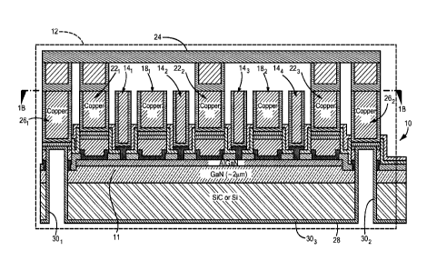
feature size masked by Schottky metal layer 14a shrinks, the thickness of the
nickel layer
in Schottky gate metal layer 14a will shrink as well to minimize undercut. For
feature
sizes less than one micron (<1 gm) as defined by Schottky gate metal 14a the
thickness of
the deposited Ni of Schottky contact gate metal layer 14a is here for example
likely to be <
100 nm .
[0078] The formation of the gate electrode structures 141-144 is shown in more
detail in
connection with FIGS. 10A-10G. Thus, after forming dielectric layer 44, here
also SiNõ,
as shown in FIG. 10A and the openings or windows 46 in layer 44, as shown in
FIG. 10B,
as described above in connection with FIGS. 2E and 2F, a first gate metal or
Schottky
contact metal layer 14'a, here for example Ni or TiN is deposited over the
dielectric layer
44 and through the window 46 onto the exposed portion of the AlGaN layer 36 as
shown
in FIG. 10C. Next, a second gate metal layer 14"a is deposited over the first
gate metal or
Schottky contact layer, here TaN, Ta, Mo, or W, for example, as shown in FIG.
10C.
[0079] Next, either a photoresist or hard mask 45 is formed over a portion of
the surface
of the second gate contact metal 14"a in registration with the window 46, as
shown in FIG.
10D. The portion of the second gate contact metal 14"a exposed by the mask is
removed
using a dry etch, as shown in FIG. 10E. Next, using the same mask 45, a dry or
wet etch is
used to remove the exposed portions of the first gate contact or Schottky
contact metal
14'a, as shown in FIG. 10F. The mask 45 is then removed as shown in FIG. 10G.
[0080] After Schottky gate metal layer 14a formation, processing continues
with the
formation of the aforementioned electrode contacts, here copper Damascene
electrode
19
CA 03045918 2019-05-10
WO 2018/156374
PCT/US2018/017895
contacts 541-5411, as shown in FIG. 2K; an exemplary one thereof, here
electrodes 542
being shown in detail in FIG. 3A. It is noted that the formation of each
copper Damascene
electrode contacts 541-54ii occurs with the deposition of two dielectric
layers (here SiNx
layer 48 and SiO2 layer 50) as shown in FIG. 21. The first layer 48, here
SiNõ, functions as
a diffusion barrier (when copper is disposed beneath it) and an etch stop. The
second
layer, here SiO2 layer 50, is etched selectively to the first layer 48, here
SiNõ, which is
then etched to reveal gate metal layer 14a thereby foi ___________________
ming the trenches into which a gold-
free material, here copper, is subsequently deposited.
[0081] Typically, copper Damascene electrode contacts 541-54ii, are formed by
first
sputtering a thin metal seed layer (typically Ta/Cu, Ta/TaN, or TaN/Cu and
..100 nm) to
facilitate copper plating into trenches formed in the second dielectric layer.
It is noted that
the seed layer also functions as a copper diffusion barrier and as an adhesion
layer to the
dielectric. The excess copper overfill of the trenches is then removed with
chemical
mechanical polishing (CMP), which defines the metal interconnects by leaving
only metal
disposed in the trenches behind. As other copper Damascene layers are added,
this
process repeats as will be discussed below. Thus, the Damascene electrode
contacts 54k-
S4 ii, have co-planar upper surfaces.
[0082] Beginning the Damascene process described in the previous paragraph and
referring now to FIG. 2H, the dielectric layer 48, here for example, SiNx, is
deposited over
the surface of the structure shown in FIG. 2G. Referring now to FIG. 21, the
second
dielectric layer 50, here for example SiO2 is deposited over layer 48 and
patterned using
conventional silicon (Si) foundry compatible lithography and etching
techniques to form
windows 52 through selected portions of layer 50 and layer 48 and thereby
expose the top
surfaces of the electrical contact structures 421 through 427 and the finger-
like gate
electrode structures 141-144, as shown in FIG. 2J for simultaneous formation
of source,
drain and gate electrodes 541-5411 thereby completing the gate electrode
structures 141-144,
drain electrode structures 181-182, and drain electrode structures 221-223,
described above
in connection with FIG. 1A.
[0083] Referring now to FIG. 2K, after the excess metal, here Cu, has been
removed by
CMP in the Damascene process as described above, the electrode contacts 541-
5411 are
formed on the exposed top surfaces of the electrical contact structures 421
through 427 and
CA 03045918 2019-05-10
WO 2018/156374
PCT/US2018/017895
the finger-like gate electrode structures 141-144, as shown. Each one of the
electrode
contacts 541-5411 is identical in construction; an exemplary one of the
electrode contacts
541-5411, here an electrode contact 542 for an exemplary one of the source or
drain
electrode structures 181-182, 221-223, respectively, here source electrode
structure 221
being shown in FIG. 3B and an exemplary one of the gate electrode contacts,
here gate
electrode structure 141 being shown in FIG. 3A. Thus, as shown more clearly in
FIGS. 3A
and 3B, each electrode contacts 541-54ii includes in this example an upper
layer 54b of
copper having the bottom and sides lined with an adhesion and copper diffusion
barrier
layer 54a, here for example, tantalum or tantalum nitride or a combination
thereof.
14)
[0084] Thus, each one of the drain electrode structures 181-182 and each one
of the source
electrode structures 221-223 is a multi-layer, electrical contact structure in
contact with the
Group III-N semiconductor layer 26 and includes: a gold-free contact layer
420c in Ohmic
contact with the Group III-N semiconductor layer 26; a gold-free electrically
conductive
etch stop layer 42E5 electrically connected to the gold-free contact layer
420c; and, one of
the gold-free Damascene electrode contacts 542, 544, 546, 548 and 541/1.
Further, each one
of the gate electrode structures 141-144 includes a gold-free gate electrical
contact and one
of the gold-free Damascene electrode contacts 543, 545, and 547. Further, each
one of the
Damascene electrode contacts 542-5410 are identical in construction and all
eight
Damascene electrode contacts 542-5410 are formed simultaneously.
[0085] Referring now to FIG. 2L, after CMP, a dielectric layer 56, here
silicon nitride
(SiNx) is deposited over the surface and then layer 56 is covered with a
second dielectric
layer 58, here an oxide layer 58, here for example silicon dioxide.
[0086] Referring now to FIG, 2M, the layers 56 and 58 are patterned using
conventional
silicon foundry compatible lithography and etch processing techniques to have
openings or
windows 601-605 formed there-through over the source electrode structures 221-
223 (FIG.
1B) and pads 261 and 262 (FIG. 1B) and thereby expose the tops of the
electrode contacts e
541, 542, 546, 5410 and 54H, as shown.
[0087] Referring now to FIG. 2N, upper electrical interconnects 621-625 are
folined in the
windows 601-605 respectively using conventional silicon foundry compatible
processing
techniques thereby making electrical connection to electrode contacts 541-54ii
541, 542,
21
CA 03045918 2019-05-10
WO 2018/156374
PCT/US2018/017895
546, 5410 and 5411, respectively, and hence to the source electrode structures
221-223 (FIG.
1B) and pads 261 and 262 (FIG. 1B). Each one of the upper electrical
interconnects 621-
625 is constructed the same as each one of the electrode contacts 541, 542,
546, 5410 and
5411 and includes an upper layer 62b of copper having the bottom and sides
lined with an
adhesion and copper diffusion barrier layer 62a, here for example, tantalum
(Ta) or
tantalum nitride (TaN) or a combination thereof.
[0088] Referring now to FIG. 20, a dielectric layer 64, here SiNx is formed
over the
structure shown in FIG. 2M followed by a dielectric layer 66 of silicon
dioxide.
[0089] Referring to FIG. 2P, a window 68 is formed through a selected portion
of the
layers 64, 66 to expose the tops of upper electrical interconnects 621-625.
[0090] Referring now to FIG. 2Q, the conductive interconnect structure 24
(FIGS. IA,
1B) is formed like the upper electrical interconnects 621-625 includes an
upper layer 24b
of copper having the bottom and sides lined with an adhesion and copper
diffusion barrier
layer 24a, here for example, tantalum or tantalum nitride or a combination
thereof.
[0091] Referring to FIG. 2R, a dielectric layer 70, here SiNx is formed over
the surface of
the structure shown in FIG. 2Q. It should be noted that additional Cu-based
interconnect
layers, if needed, may be added in a manner identical to the Cu interconnect
layers
described above. After the addition of the final interconnect layer, a test
pad layer or
Input/Output pads (not shown) may be added for facilitate final testing or
connection to
other circuits (not shown), respectively. At this point front-side processing
is complete.
[0092] After the completion of front-side processing, and referring now to
FIG. 2S, the
back-side processing begins. More particularly the wafer is mounted face down
on a
temporary carrier, not shown, the wafer is then thinned, here for example to
50 or 100
microns. The exposed bottom surface of such structure is masked to expose
portions of
the bottom of the substrate 32 under the electrode contacts 541 and 54n. Next,
via holes
72 are formed in the exposed portions by etching from the bottom of the SiC or
Si
substrate 32 using a dry fluorine-based etch, here, for example sulfur
hexafluoride (SF6).
22
CA 03045918 2019-05-10
WO 2018/156374
PCT/US2018/017895
[0093] Referring now to FIG. 2T, the bottom surface of substrate 32 is exposed
to a dry
chlorine-based etch, here for example a combination of boron tri-chloride
(BC13) and
chlorine (C12), to continue the depth of via holes 72 (as indicated by the
arrows 74) by
etching through the exposed portions of the Group III-N layer 34 and then
through
exposed inner portions of the Ti or Ta layer 42a, then through inner portions
of the
aluminum-based layer 42b, then through exposed inner portions of the metal
nitride layer
42c of the Ohmic contact structures 420c of the electrode contacts 541 and
54ii; the
etching then stopping at the etch stop layer 42E5 on the electrical contact
structures 42
under the electrode contacts 541 and 5411, as indicated.
[0094] Next, referring to FIG. 2U, the bottom of the structure of FIG. 2T has
the
conductive layer 28 (FIG. 1A) disposed on the bottom of substrate 32 and into
via hole,
72. Here, for example, the layer 28b is copper with an adhesion and copper
diffusion
barrier layer 28a, here for example, tantalum or tantalum nitride or a
combination thereof
(as shown in FIG. 2U') to form the conductive vias 301 and 302 (FIG. IA) and
aground
plane conductor 303. The conductive vias 301 and 302 electrically interconnect
the ground
plane conductor 303 to the front side metallization layers and ultimately to
the interconnect
source electrode structures 221-223 through etch stop layer 42E5 to bottom of
electrode
contacts 541 and 54ii (FIGS. lA and 1B). It should be understood that the
conductive vias
301 and 302 and ground plane 303 can have layer 28 comprised of alternate
metals here, for
example a gold (Au) layer 28b, and a titanium (Ti) or titanium/platinum
(Ti/Pt) layer 28a.
In this case, the back-side processing would be performed in an area where
gold would not
present any contamination problems.
[0095] Thus, here, in the embodiment described above in connection with FIGS.
2A
through 2U, after front-side processing and back-side wafer thinning, a back-
side via hole
72 is formed using chemical dry etching with a two-step etch process that
terminates on
the electrically conductive etch stop layer 42E5. In the first step of the via
hole etch
process, via holes are formed in exposed portions of the bottom of the SiC or
Si substrate
layer 32 using a dry fluorine-based etch for example, sulfur hexafluoride
(SF6). This
fluorine-based etch stops selectively on Group III-N layer 34 such as gallium
nitride
(GaN) and aluminum nitride (AIN). In the second step, the bottom surface of
the exposed
Group III-N layer in the via hole 72 is exposed to a dry chlorine-based etch,
for example a
combination of boron tri-chloride (BC13) and chlorine (C12). This chlorine-
based back-
23
CA 03045918 2019-05-10
WO 2018/156374
PCT/US2018/017895
side via hole 72 dry etch continues the via hole etching through the Group III-
N layers 34
and 36 (in the example shown in FIG. 2, "off' mesa etches only need to etch
through
Group III-N layer 34 after etching through substrate layer 32) and the metal
to
semiconductor electrical contact structure and terminates on the conductive
etch stop layer
42Es here for example nickel or molybdenum or platinum.
[0096] Referring now to FIG. 5A through 5C, here an embodiment is described of
a
portion of a MMIC structure 10', here for example having, as shown in more
detail in
FIG. 5A, a multi-gate HEMT FET, having: electrode contacts 542, 546 and 5410
disposed
on electrical contact structures 427, 424 and 426, respectively, as shown to
provide gold-
free source electrode structures 221-223 in Ohmic contact with Group III-N
semiconductor
layer 36 and interconnected with gold-free conductive vias 301-303 (FIG. 5C)
passing
through the substrate 32, the Group III-N layer 34, and the Group III-N
semiconductor
layer 36 to the conductive layer 28 formed on the bottom of the structure 10';
electrode
contacts 544, and 548 disposed over electrical contact structures 423, and
425, respectively,
as shown to provide gold-free drain electrodes structures 181, 182 in Ohmic
contact with
Group III-N semiconductor layer 36 and interconnected to the gold-free drain
pad 20 (FIG.
1B) and electrode contacts 543, 545, 547 and 549 disposed over gold-free gate
electrode
structures 141-144, respectively in Schottky contact with the Group III-N
semiconductor
layer 36 and connected to gate pad 16 (FIG. 1B). The structure 10' includes: a
resistor R,
here for example tantalum nitride (TaN), having a pair of electrodes (the
opposing ends of
the resistor R) R1 and R2; one of the electrodes, R1, being connected to
electrode contact
5411, electrical contact 427 and then to the conductive layer 28 by a
conductive via 304
(FIG. 5C) passing through passing through the substrate 32, and the Group III-
N layer 34
to the gold-free conductive layer 28 formed on the bottom of the structure
10', and the
other electrode R2 being disposed on electrode 5412, which is disposed on
electrical
contact 428, which is disposed on Group III-N layer 34; and a capacitor C
having a
bottom plate Cl formed by electrode contact 541 and electrical contact
structure 421 (FIG.
5A) and interconnected to a conductive via 305 passing through the substrate
32, and the
Group III-N layer 34 to the gold-free conductive layer 28 formed on the bottom
of the
structure 10'; an upper plate C2, here an electrical interconnect 54a having a
copper layer
54b lined with layer 54a, here for example, tantalum or tantalum nitride or a
combination
thereof; and a dielectric 75, here for example silicon nitride, disposed
between the upper
plate C2 and the bottom plate Cl, as shown. Finally, it should be noted that
in many
24
CA 03045918 2019-05-10
WO 2018/156374
PCT/US2018/017895
circuit designs, the capacitor C and resistor R need not be connected to
conductive vias
30.
[0097] It is noted that the thickness of the copper forming the lower plate Cl
of the
capacitor C and used for the resistor R is thicker than that used for the
source electrode
structures 221, 222 and 223 and drain electrode structures 181 and 182 for two
reasons:
First, the trenches foimed during Damascene processing have to be deeper
(unless ion
implantation isolation instead a mesa as noted above, which is not shown, is
used to enable
planar structures) to enable "off' mesa 11 (FIGS. 1B and 2A) vertical
interconnects to
"on" mesa 11 electrical contact structures 42. Second, all contacts formed
during metal
layer deposition terminate at the same level on the upper surface of the layer
due to the
CMP process.
[0098] It is also noted that the electrical contact structures 421-428,
described above, are
formed in the same manner described above in connection with FIGS. 2A-2T.
Thus, the
source electrode structures 221, 222 and 223 and drain electrode structures
181 and 182 are
in Ohmic contact with the Group III-N semiconductor layer 36 and the gate
electrode
structures 141, 142 and 143 are in Schottky contact with the Group III-N
semiconductor
layer 36.
[0099] Next, the back-side processing proceeds as in FIGS. 2S and 2T. More
particularly,
the wafer is mounted face down on a temporary carrier, not shown, the wafer is
thinned,
here for example to 50 or 100 microns. The exposed bottom surface of such
structure is
masked with mask 78 and processed using conventional silicon compatible
processing
techniques to expose portions of the bottom of the substrate 32 disposed under
the central
or inner surface portions of the electrical contact structures 421, 422, 424,
426 and 427, as
shown, followed by, first a dry fluorine-based etch, here, for example SF6, as
described
above in connection with FIG 2S to etch via holes 72 through exposed portions
of the
substrate 32 and then a dry chlorine-based etch, here for example a
combination of
boron tri-chloride (BC13) and chlorine (C12), to continue the depth of via
holes 72 by
etching through the exposed portions of Group III-N layers 34 and 36, then
through the
central or inner portions 798) , as shown for an exemplary one of the
electrical contact
structures, here electrical contact structure 422 (FIG. 5B') of the bottom
surface of the
electrical contact structures 421, 422, 424, 426 and 427 and stopping at the
etch stop layer
CA 03045918 2019-05-10
WO 2018/156374
PCT/US2018/017895
42Es (here for example nickel or molybdenum or platinum) of structures, as
described
above in connection with FIG. 2T. It is noted that outer portions 79op of the
bottom
surface of the electrical contact structures 422, 424, 426 remain un-etched
and therefore
remain in ohmic contact with the Group III-N layer 36.
[0100] Next, referring to FIG. 5C, the mask 78 is removed and the back-side
process is
performed as described in connection with FIG. 2U. Thus, the bottom of the
structure of
FIG. 5B has conductive layer 28 formed over it and over the sides and bottom
surface of
then extended via holes 72, as described above in connection with FIG. 2U' to
form
conductive vias 301-305 over the exposed electrically conductive etch stop
layers 42Es to
electrically interconnect the source electrode structures 221-223, the bottom
plate Cl of
capacitor C and the electrode R1 of resistor, as shown.
[0101] It is noted that here the electrical contact structures 42' could be a
single Ohmic
contact layer 42'oc, here a silicide layer, here for example nickel silicide
(NiSi) or cobalt
silicide (CoSi2), as shown in FIG. 5A'. Further, the silicide layer Ohmic
contact structure
42'oc may also be doped to further improve contact resistance. In the case of
NiSi, for
example it could be doped with phosphorus (P), arsenic (As), antimony (Sb) or
a
combination thereof. In order to form the Ohmic contact structure 42'oc, Si
and Ni or Co
is deposited, etched back and then alloyed. In the case of NiSi the alloy temp
here for
example is ¨450 C. In the case of CoSi2 a two-step anneal, here for example
¨550 C
followed by ¨700 C, is used. In order to facilitate better Ohmic contact to
the Group III-N
layer 36, the silicide layer, Ohmic contact structure 42'oc may be recessed
into the Group
III-N semiconductor layer 36 so that the bottom surface of silicide layer
Ohmic contact
structure 42'oc is 2-20 nm from the bottom surface of the Group III-N layer
36. It is noted
that the etch stop layer 42Es is disposed on the Ohmic contact structure
42'oc, as shown.
Here the electrical contact structure includes an Ohmic contact structure
42'oc having an
etch stop layer 42E5 on the Ohmic contact structure 42'oc.
[0102] Referring now to FIGS. 6A-6D another embodiment is described. Here,
again, as
in FIG. 6A, a structure 10" is shown having substrate 32 here for example, Si
or SiC; a
mesa shaped (defined by etching or implant isolation, as noted above), Group
III-N
semiconductor layer 34 on an upper portion of the substrate 32, here Group III-
N layer 32
is, for example, a layer of gallium nitride (GaN) having a thickness of
approximately 1-5
26
CA 03045918 2019-05-10
WO 2018/156374
PCT/US2018/017895
microns over the upper surface of the substrate 32, as shown, and a Group III-
N
semiconductor layer 36, here Al.Gai-,N, for example having a thickness of
approximately
5-30 nm, on the upper surface of Group III-N layer 34. As will be described
below, the
structure 10" will be processed to form a multi-gate HEMT. Here, however,
apertures 80
are etched, using conventional silicon foundry compatible subtractive
patterning
(lithography and etching) techniques and here, for example a combination of
boron tri-
chloride (BC13) and chlorine (C12) dry etching, in portions of the Group III-N
layers 34 and
36 where electrically conductive vias 90, to be described in connection with
FIGS. 6B and
6C, are to be formed to electrically interconnect the sources electrode
structures 221-223
to (FIG. 1B).
[0103] Referring to FIG. 6B, the apertures 80 are filled with a semiconductor
or dielectric
or metal material 82 that can be dry etched in fluorine containing gasses,
here for example
SiNx, SiO2, molybdenum or polysilicon or a combination thereof. The structure
is
processed as described above in connection with FIGS. 2B-2K to form electrical
contact
structures 42"1-42"5; it being noted that here the electrical contact
structures 42"1-42"5 do
not include a separate etch stop layer, such a etch stop layer 42Es as
described above in
connection with FIGS. 2A-2U; rather, in this embodiment the aluminum or Si
doped
aluminum A11_Si,, layer 42b (where the Si doping, x, is typically 0.05) layer
of the
Ohmic contact structure 42"oc of the electrical contact structures 42"1-42"5
functions, as
will be described in connection with FIG. 6B, as an etch stop layer. Electrode
contacts
541, 543, 545, 547 and 549, respectively are disposed on the top of Ohmic
contact structures
420c1-420c5, respectively, as indicated. Electrical contact structures 42"1,
42"3 and 42"5
are for the source electrode structures 221-223 and electrical contact
structures 42"2 and
42"4 are drain electrode structures 181, 182 (FIG. 1B). It is noted that the
bottom surface
of the electrical contact structures 42"1, 42"3 and 42"5 are larger in surface
area than the
surface area of the semiconductor or dielectric or metal material 82, with the
outer surface
portions of the electrical contact structures 42"1, 42"3 and 42"5 being in
Ohmic contact
with the Group III-N semiconductor layer 36, as shown. Gate electrode
structures 141-144
are in Schottky contact with the Group III-N semiconductor layer 36, as shown,
and have
thereon electrode contacts 542, 544, 546, and 548, as shown.
[0104] The Ohmic contact structure layers 42a, 42b, and 42c of the electrical
contact
structures 42"1-42"5 and the electrode contacts have been described above in
connection
27
CA 03045918 2019-05-10
WO 2018/156374
PCT/US2018/017895
with FIG. 3B with the Ohmic contact structure 420C1-42005 having: a bottom
layer 42a of
Ti or Ta (which may be recessed into the upper surface portions of the Group
III-N
semiconductor layer 36); a middle layer 42b of an aluminum-based layer, here
aluminum
or Si doped aluminum Ali,Six layer; and an upper layer 42c of tantalum or
metal nitride
layer, here for example tantalum (Ta), tantalum nitride (TaN) or titanium
nitride (TiN) on
the aluminum or Si doped aluminum Ali_xSix layer; and the electrode contacts
541-549
having an electrically conductive metal interconnect contact, here for example
copper
having the sides and bottom lined with a diffusion barrier layer, here for
example,
tantalum or tantalum nitride or a combination thereof. Thus, as will be
discussed more
it) detail below, relating to the back-side processing, it is noted that in
this embodiment,
there is no separate etch stop layer 42Es (described above in connection with
FIGS. 2A-
2U); rather, because of the fluorine chemical etcharit used to form the vias
90 (FIG. 6C) in
this embodiment, the etch stop layer is provided by layer 42b, here for
example aluminum
(or Si doped Aluminum Ali,Six, of electrical contact structures 42".
[0105] Next, the back-side processing proceeds as in FIG. 2U. More
particularly the
wafer is mounted face down on a temporary carrier, not shown, the wafer is
thinned, here
for example to 50 or 100 microns. The exposed bottom surface of such structure
is
masked by a mask 96 (FIG. 6C) to expose portions of the bottom of the
substrate 32 under
the source electrode structures 221-223. It should be noted that outer
peripheral portions of
the semiconductor or dielectric or metal material 82 are covered by the mask
96; and
hence under the inner portions 811p (FIG. 6C') of the electrical contact
structures 42 while
the other portions 810p of the electrical contact structures 42 remain in
Ohmic contact with
layer 36. Next, vias 90 are etched using a dry fluorine-based etch, here for
example SF6 to
etch the vias 90 through the substrate layer 32 and through the inner portions
of the
material 82 (here for example SiNx, 5i02, molybdenum or poly silicon in FIG.
6C'), inner
portions 811p of the bottom layer 42a of Ti or Ta (which may be recessed into
the upper
surface portions of the Group III-N semiconductor layer 36) and then stopping
at inner
portions of the Aluminum-based layer 42b whose fluorine-based etch byproducts
are non-
volatile. Thus, here there is no additional (separate) etch stop layer 42Es;
rather layer 42b
functions as an etch stop layer.
[0106] Next, referring to FIG. 6D, the bottom of the structure of FIG. 6C has
a conductive
layer 28, here for example copper-based, is formed over it and over the sides
and bottom
28
CA 03045918 2019-05-10
WO 2018/156374
PCT/US2018/017895
surface of then extended via holes 90 to form conductive vias 96 and a ground
plane
conductor 95, as described above in connection with FIG. 2U, for the structure
to
electrically interconnect the inner or central portions of the electrical
contact structures
42" as shown, and therefore interconnect the source electrode structures 221-
223. In this
embodiment, the Group III-N material is etched from the front-side of the
wafer, as
described above in connection with FIG. 6A prior to back-side processing and
via 90
formation. The apertures 80 (FIG. 6A) are then filled with a material layer 82
(here for
example SiNx, SiO2, molybdenum or polysilicon) that can be etched with
fluorine-based
dry etch chemistries. Assuming that all the layers that need to be etched to
form the via 90
are now the substrate 32 (silicon, silicon carbide (SiC), silicon dioxide
(SiO2), silicon
nitride (SiNx) or a combination thereof) and the aperture semiconductor or
dielectric or
metal material 82 (here for example SiNx, SiO2, molybdenum or polysilicon),
those layers
can now all be etched using the fluorine-based etchants. As a result, a
fluorine-based etch
is then used for the entire via etch process.
[0107] Referring now FIG. 6D' another embodiment is described. In this
embodiment the
via 96 is etched wider than in FIG. 6D; however, here again the etching stops
at the inner
portions of the Aluminum based layer 42b. Thus again there is no additional
(separate)
etch stop layer 42Es; rather layer 42b functions as an etch stop layer. In
this case (Fig.
6D') there is no remaining dielectric layer 82 in the via 90 (as shown in Fig.
6C').
[0108] Referring now to FIGS. 7A-7G, another embodiment is shown. Here the
structure
10¨ shown in FIG. 2B is processed as described in connection with FIG. 2C
except only
windows 402-406 are formed, as shown. After forming windows 402-406, an etch
stop
layers 42Es', here for example, silicon dioxide or SiN, are formed using
conventional
silicon (Si) foundry compatible (subtractive) lithography and etch processing
techniques,
on the inner surface portions of layer 36 exposed by the windows 402, 404,
406; it being
noted in FIG. 7B that outer surface portions of the exposed surface of layer
36 are void of
the etch stop layers 42E5'. Alternately, but not shown, etch stop layers
42Es', could be
formed on the inner surface portions of layer 36 exposed by all windows 40.
[0109] Referring now to FIG. 7C, layers 42a, 42b and 42c are now formed over
the etch
stop layers 42E5'; it being noted that outer peripheral portions of the layers
42a, 42b and
42c are in direct contact with layer 36. Thus, after an anneal process
described above in
connection with FIGS. 4A, 4A' and 4B, 4B', Ohmic contact is formed between the
outer
29
CA 03045918 2019-05-10
WO 2018/156374
PCT/US2018/017895
peripheral portions of layers 42a, 42b and 42c and Group III-N layer 36. It
should be
noted that here the electrical contact structures 42-1, 42"3 ,and 42-5 include
an etch stop
layer, here etch stop layer 42Es', that is under the inner portions of layers
42a, 42b and
42c; rather than on top of layers 42a, 42b, and 42c. Thus, while, as noted
above in
connection with FIG. 3B where the electrical contact structure 42" included
etch stop
layer 42Es on top of layer 42c (on top of the electrical contact structure
42); here, as shown
in FIG. 3B', the etch stop layer 42E5' of the electrical contact structure 42'
used in FIGS.
7A-7F is under the inner or central portion of layer 42a of the electrical
contact structure
42¨).
[0110] It is also noted in FIG. 7C that electrode contacts 541-549
simultaneously form the
upper layers of the source electrode structures 221-223, drain electrode
structures 181, 182,
and gate electrode structures 141-144, as shown.
[0111] Referring now to FIG. 7D, after the completion of front-side
processing, and
referring now to FIG. 2S, the back-side processing begins. More particularly
the wafer is
mounted face down on a temporary carrier, not shown, the wafer is then
thinned, here for
example to 50 or 100 microns. The bottom surface of the structure is masked
with
windows therein disposed under the etch stop layers 42E5'. An etchant, here
for example,
fluorine, is used to etch via 102 through the substrate 32, as shown.
[0112] Referring now to FIG. 7E, a chlorine-based etchant such as BC13 and C12
are used
to extend the vias 102 to via 102'; as shown, such etching stopping at the
etch stop layers
42Es', as shown. Next, the etch stop layer 42E5' is removed from the bottom of
the via hole
102' using dry etch chemistries that are fluorine-based when either SiO2 or
SiNx is used as
a layer 42E5' etch stop. Fluorine-based wet etches are suitable for removing
SiO2 and
Al2 0 3 layer 42Es' etch stops, and some SiNx layer 42E5' etch stops, as shown
in FIG. 7F.
[0113] Referring now to FIG. 7G, a conductive layer 28 is formed over the
bottom of the
structure as described above in connection with FIG. 2U to electrically
interconnect the
source electrode structures 221-223.
[0114] Referring now to FIGS. 8A-8F another embodiment is shown for forming an
Ohmic contact to one of the source electrode structures and the connection of
the source
electrode structure to back-side metallization conductive layer 28. Thus,
after forming the
CA 03045918 2019-05-10
WO 2018/156374
PCT/US2018/017895
dielectric layer 38 on the upper surface of the AlGaN layer 36, as shown in
FIG. 8A, a
window 200 is formed through the dielectric layer 38, underlying portions of
AlGaN layer
36, and GaN layer 34 to the surface of the substrate 32, as shown in FIG. 8B,
here using
conventional lithography and dry etch processes, here for example the chlorine-
based
etchants BC13 and C12.
[0115] Next, referring to FIG. 8C, the electrical contact structure 42' having
layers 42a,
42b and 42c of the Ohmic contact structure 420c are sequentially deposited and
patterned
as shown using conventional lithographic-etching process as described above in
connection with FIG. 2D, the Ohmic contact structure 420c having: a bottom
layer 42a of
titanium (Ti) or tantalum (Ta); a layer 42b for example, aluminum or Si doped
aluminum
Ali,Six (where the Si doping, x, is typically 0.05) on the layer 42a; and a
layer 42c, for
example tantalum (Ta) or a metal nitride, here for example titanium nitride
(TiN). Next,
the anneal processes described above is used to form Ohmic contact regions 110
(FIG. 8C
between the Ohmic contact structure 420c and sidewalls of the AlGaN layer 36.
Next, the
dielectric layers 44 and 48 are formed as shown in FIG. 8D, as described above
in
connection with FIGS. 2F through 2H.
[0116] Next, the Damascene process begins by depositing the dielectric layer
50 as
described above in connection with FIGS. 21, as shown in FIG. 8E, followed by
the
formation of the electrical interconnect including, in this example the upper
layer 54b of
copper having the bottom and sides lined with an adhesion and copper diffusion
barrier
layer 54a, here for example, tantalum or tantalum nitride or a combination
thereof as
described above in connection with FIGS. 21-2L, resulting in an exemplary one
of the
above described Damascene electrode contacts 541-54i , here indicated without
a
subscript as 54, as shown in FIG. 8F.
[0117] The processing continues as described above in connection with FIGS. 2M-
2R
after which the back-side processing begins as described above in connection
with FIGS.
6A-6D. More particularly, the wafer is mounted face down on a temporary
carrier, not
shown, the wafer is thinned, here for example to 50 or 100 microns. The
exposed bottom
surface of such structure is masked to expose portions of the bottom of the
substrate 32
under the source electrode structure. Next, vias 90 are etched using a dry
fluorine-based
etch, here for example SF6 to etch the vias 90 through the substrate layer 32
and through
31
CA 03045918 2019-05-10
WO 2018/156374
PCT/US2018/017895
the bottom layer 42a of Ti or Ta and then stopping at the aluminum-based layer
42b
whose fluorine-based etch byproducts are non-volatile. Thus, here there is no
additional
(separate) etch stop layer 42Es; rather layer 42b functions as an etch stop
layer, as shown
in FIG. 8G.
[0118] Next, referring to FIG. 8H, the bottom of the structure of FIG. 8G has
a conductive
layer 28 in electrical connection with the layer 42b of the electrical contact
structure 42',
as described above in connection with FIGS. 2S-2U.
[0119] Referring now to FIGS. 9A-9E, another embodiment is shown. Here, after
forming the dielectric layer 38 on the upper surface of the AlGaN layer 36, as
shown in
FIG. 9A, the window 200 is formed through the dielectric layer 38, underlying
portions of
AlGaN layer 36, and GaN layer 34 to the surface of the substrate 32, as shown
in FIG. 9B,
here using conventional lithography and dry etch processes, here for example
the chlorine-
based etchants BC13 and C12.
[0120] Next, the window 202 is etched with a fluorine-based dry etchant that
laterally
etches dielectric layer 38 (as shown in FIG. 9C) to expose a surface portion
of Group III-N
semiconductor layer 36 around the edge of the window 200 (as shown in FIG.
9B).
[0121] Next, as shown in FIGS. 9D and 9E, layers 42a, 42b, 44 and 48 are
formed as
described in connection with FIGS. 8C and 8D after which the process continues
as
described above in connection with FIGS. 8E and 8F.
[0122] A number of embodiments of the disclosure have been described.
Nevertheless, it
will be understood that various modifications may be made without departing
from the
spirit and scope of the disclosure. For example, the metal to semiconductor
Ohmic contact
structure 420E' may comprise a two or more layer stack of Al with Ta, Ti, TiN,
Pt, Ni, Si,
AlSi, W, or Mo such as Ta/A1, Ti/A1, Ta/Al/Ta, Ta/ AliSi1 /Ta, Ta/Al/TiN
Ta/Al/Ni,
Ti/Al/Ni, Ta/A1, Ti/A1, Ti/Al/W, Ti/Al/Mo, Ti/Al/Pt. Furthermore, the
structure shown in
FIG. 2J may be removed from gold-free fabrication area prior to forming the
electrode
contacts 54 in which case the electrode contacts 54 may be gold.
[0123] It should now be appreciated a semiconductor structure according to the
disclosure
includes: a substrate; a Group III-N semiconductor layer disposed on the
substrate; a
32
CA 03045918 2019-05-10
WO 2018/156374
PCT/US2018/017895
multi-layer, electrical contact structure in contact with the Group III-N
semiconductor
layer, the electrical contact structure comprising: a gold-free contact layer
in contact with
the Group III-N semiconductor layer and a gold-free electrically conductive
etch stop
layer electrically connected to the gold-free contact layer; and an
electrically conductive
via passing through the substrate to the etch stop layer. The semiconductor
structure may
include one or more of the following features independently or in combination
with
another feature to include: wherein the multi-layer, electrical contact
structure comprises
an aluminum-based layer disposed over the gold-free contact layer; wherein the
gold-free
contact layer is in direct contact with the Group III-N semiconductor layer
and wherein the
gold-free contact layer and the aluminum-based layer have physical annealing
properties
enabling annealing with the Group III-N semiconductor layer at a temperature
less than
660 degrees to form an Ohmic contact with the Group III-N semiconductor layer;
an
electrode contact electrically connected to the multi-layer electrical contact
structure and
wherein the multi-layer, electrical contact structure and the electrode
contact provide a
source, drain or gate electrode structure; wherein the electrode contact is a
gold-free
electrode contact; wherein the etch stop layer comprises aluminum, nickel,
molybdenum,
platinum, or aluminum; wherein the electrical contact structure comprises a
two or more
layer stack of Al with Ta, Ti, TiN, Pt, Ni, Si, AlSi, W, or Mo; wherein the
electrical
contact structure comprises a metal silicide; wherein the metal silicide is
CoSi2 or NiSi;
wherein the metal silicide is recessed within the Group III-N semiconductor
layer; wherein
the silicide is doped with phosphorus (P), arsenic (As), or antimony (Sb); and
wherein the
multi-layer structure is recessed within the Group III-N semiconductor.
[0124] It should now be appreciated a method for forming a semiconductor
structure
according to the disclosure includes: providing a substrate with a Group III-N
semiconductor layer disposed on the substrate; forming a multi-layer,
electrical contact
structure in contact with the Group III-N semiconductor layer, the electrical
contact
structure, comprising: a gold-free contact layer in contact with the Group III-
N
semiconductor layer; and a gold-free electrically conductive etch stop layer
electrically
connected to the contact layer; and, forming an electrically conductive via
passing through
the substrate to the etch stop layer. The method may include one or more of
the following
features independently or in combination with another feature to include:
wherein the
multi-layer, electrical contact structure comprises an aluminum-based layer
disposed over
the gold-free contact layer; wherein the gold-free contact layer is formed in
direct contact
33
CA 03045918 2019-05-10
WO 2018/156374
PCT/US2018/017895
with the Group III-N semiconductor layer and wherein the contact layer and the
aluminum-based layer are annealed at a temperature less than 660 degrees to
form an
Ohmic contact with the Group III-N semiconductor layer; and wherein the multi-
layer,
electrical contact structure includes an electrode contact electrically
connected to the
multi -lay er, electrical contact structure; wherein the multi-layer,
electrical contact
structure and the electrode contact provide a source, drain or gate electrode
structure; and
wherein the electrode contact is formed as a gold-free electrode contact.
[0125] It should now be appreciated a semiconductor structure according to the
disclosure
includes: a Group III-N semiconductor layer; and an electrical contact
structure comprises
a metal silicide, the metal silicide being in Ohmic contact with the Group III-
N
semiconductor layer. The structure may include a gold-free etch stop layer
electrically
connected to the electrical contact structure; and an electrically conductive
via electrically
connected to the electrically conductive etch stop layer.
[0126] It should now be appreciated a method for forming an electrically
conductive
Ohmic contact in contact with a group III-N layer according to the disclosure
includes:
forming an Ohmic contact between the electrical contact structure and a Group
III-N
semiconductor layer, comprising: forming a metal nitride between a first metal
of the
electrical contact structure and the Group III-N semiconductor layer and
diffusing a
second metal of the electrical contact structure into the first metal and to
an upper surface
of the Group III-N semiconductor layer including: preventing intermixing with
a third
metal or metal nitride of the electrical contact. The method may include one
or more of
the following features independently or in combination with another feature to
include:
wherein the intermixing preventing comprises: forming and annealing the first
and second
metals of the electrical contact structure during Ohmic contact formation
prior to
deposition of the third metal or metal nitride of the Ohmic contact; wherein
the
intermixing preventing comprises: forming a partially oxidized interlayer
between the
second metal and third metal; and wherein the intermixing preventing
comprises: forming
the third metal as a metal nitride during the electrical contact structure
metal deposition
process.
[0127] It should now be appreciated a semiconductor structure according to the
disclosure
includes: a substrate; a Group III-N layer on an upper surface of the
substrate, the Group
34
CA 03045918 2019-05-10
WO 2018/156374
PCT/US2018/017895
III-N layer having a window passing through the Group III-N layer to the upper
surface of
the substrate; and an electrical contact structure disposed in the window, on
the upper
surface of the substrate and in Ohmic contact with the Group III-N layer.
[0128] It should now be appreciated a semiconductor structure according to the
disclosure
includes: a substrate; a Group III-N layer on a upper surface of the
substrate, the Group
III-N layer having a window passing through the Group III-N layer to the upper
surface of
the substrate, such window exposing sidewall of the Group III-N layer; and an
electrical
contact structure disposed in the window and in Ohmic contact with the exposed
sidewalls
of the Group III-N layer. The semiconductor structure may also include a gold-
free etch
stop layer electrically connected to the electrical contact structure; and an
electrically
conductive via electrically connected to the electrically conductive etch stop
layer.
[0129] Accordingly, other embodiments are within the scope of the following
claims.
35