Note: Descriptions are shown in the official language in which they were submitted.
HIGHER-LEVEL CLOCK AND DATA RECOVERY (CDR) IN
PASSIVE OPTICAL NETWORKS (PONS)
BACKGROUND
[0001] A PON is a system for providing network access over a final portion
of a
telecommunications network. A PON is a P2MP network comprising an OLT at a CO,
an ODN,
and ONUs at user premises. PONs may also comprise RNs located between the OLTs
and the
ONUs, for instance, at an end of a road where multiple customers reside.
[0002] In recent years, TDM PONs such as GPONs and EPONs have been deployed
worldwide for multimedia applications. In TDM PONs, the total capacity is
shared among multiple
users using a TDMA scheme, and as a result the average bandwidth for each user
may be below
100 Mb/s. EPONs use WDM and provide rates up to 10 Gb/s. Next-generation EPONs
may be
required to implement 100 Gb/s due to increasing customer demands.
[0003] Future approaches include four-channel WDM networks with 25 Gb/s bit
rates per
wavelength channel and fewer-channel WDM networks with even higher bit rates
per single
channel. As bit rate demand continues to increase, bandwidth restrictions
meant to efficiently use
existing devices may result in severe 1ST. ISI is a significant challenge for
CDR for high-speed
PONs. In particular, for high-speed, upstream, burst-mode transmissions in
PONs, a converging
speed and a quality of the CDR can significantly affect data transmission
quality.
SUMMARY
[0004] In one embodiment, the disclosure includes an apparatus comprising:
an OE component
configured to convert an optical signal with a first modulation format to an
analog electrical signal;
an ADC coupled to the OE component and configured to convert the analog
electrical signal to a
first digital signal; and a CDR sub-system coupled to the OE component and
configured to:
equalize the first digital signal into a second digital signal with a second
modulation format,
wherein the second modulation format has more levels than the first modulation
format; and
perform CDR on the second digital signal. In some embodiments, the apparatus
further comprises
a PR-MLSE component coupled to the CDR sub-system and configured to equalize
the second
digital signal into a third electrical signal with the first modulation
format; the PR-MLSE
1
CA 3046714 2020-02-11
component is further configured to further equalize the second digital signal
using PR-MLSE; the
CDR sub-system comprises an FFE, a decision component, a subtractor, and a tap
weight updater
that form a feedback loop, and wherein the PR-MLSE component is outside the
feedback loop; the
first modulation format has two levels for an NRZ signal and the second
modulation format has
three levels; the first modulation format has four levels for a PAM4 signal
and the second
modulation format has seven levels; the CDR sub-system comprises an FFE
configured to: perform
the CDR for phase adjustment; and perform equalization for ISI compensation;
the FFE is further
configured to adaptively track frequency offset and jitter; the CDR sub-system
is further
configured to perform equalization until an MSE of an equalized signal is
below a predetermined
threshold; the apparatus is an OLT, and wherein the analog electrical signal
is a burst-mode signal;
the OE component is a PD, a TIA, or a combination of the PD and the TIA.
[0005] In another embodiment, the disclosure includes an apparatus
comprising: a CDR sub-
system comprising: an FFE; a decision component coupled to the FFE; a
subtractor coupled to the
FFE and the decision component; and a tap weight updater coupled to the
subtractor and the FFE;
and a PR-MLSE component coupled to the CDR sub-system. In some embodiments,
the apparatus
further comprises an ADC coupled to the CDR sub-system; the apparatus further
comprises a VCO
coupled to the ADC; the apparatus further comprises a TIA coupled to the ADC;
the apparatus
further comprises a PD coupled to the TIA; the apparatus further comprises a
decoder coupled to
the PR-MLSE component coupled to the PR-MLSE component.
[0006] In yet another embodiment, the disclosure includes a method
comprising: converting
an optical signal with a first modulation format to an analog electrical
signal; converting the analog
electrical signal to a first digital signal; equalizing the first digital
signal into a second digital signal
with a second modulation format, wherein the second modulation format has more
levels than the
first modulation format; and performing CDR on the second digital signal. In
some embodiments,
the method further comprises equalizing the second digital signal into a third
electrical signal with
the first modulation format using PR-MLSE; the method further comprises
performing
equalization until an MSE of an equalized signal is below a predetermined
threshold.
[0007] For the purpose of clarity, any one of the foregoing embodiments may
be combined
with any one or more of the other foregoing embodiments to create a new
embodiment within the
scope of the present disclosure.
2
CA 3046714 2020-02-11
[0008] These and other features will be more clearly understood from the
following detailed
description taken in conjunction with the accompanying drawings and claims.
BRIEF DESCRIPTION OF THE DRAWINGS
[0009] For a more complete understanding of this disclosure, reference is
now made to the
following brief description, taken in connection with the accompanying
drawings and detailed
description, wherein like reference numerals represent like parts.
[0010] FIG. 1 is a schematic diagram of a PON.
[0011] FIG. 2A is a schematic diagram of a data communication system.
[0012] FIG. 2B is a schematic diagram of the receiver in FIG. 2A.
[0013] FIG. 3 is a graph illustrating a two-level equalization erroring in
the FFE in FIG. 2B.
[0014] FIG. 4 is a table illustrating a two-level converging time for
different clock phase errors
for the FFE in FIG. 2B.
[0015] FIG. 5 is a graph illustrating a four-level equalization error in
the FFE in FIG. 2B.
[0016] FIG. 6 is a table illustrating a four-level converging time for
different clock phase errors
for the FFE in FIG. 2B.
[0017] FIG. 7 is a schematic diagram of a higher-level CDR receiver
according to an
embodiment of the disclosure.
[0018] FIG. 8 is a graph illustrating phase error and 1ST.
[0019] FIG. 9 is a schematic diagram of a device according to an embodiment
of the disclosure.
[0020] FIG. 10A is a diagram illustrating a two-level NRZ signal prior to
three-level CDR.
[0021] FIG. 10B is a graph illustrating a three-level NRZ signal after
higher-level CDR
performed in FIG. 7 according to an embodiment of the disclosure.
[0022] FIG. 11A is a diagram illustrating a four-level PAM4 signal prior to
seven-level CDR.
[0023] FIG. 11B is a graph illustrating a seven-level PAM4 signal after
higher-level CDR
according to an embodiment of the disclosure.
[0024] FIG. 12 is a graph illustrating an equalization error for the FFE in
FIG. 7 equalizing a
two-level NRZ signal using three-level equalization according to an embodiment
of the disclosure.
[0025] FIG. 13 is a table illustrating a converging time for the FFE in
FIG. 7 equalizing a two-
level NRZ signal using three-level equalization according to an embodiment of
the disclosure.
3
CA 3046714 2020-02-11
[0026] FIG. 14 is a graph illustrating an equalization error for the FFE in
FIG. 7 equalizing a
four-level PAM4 signal using seven-level equalization according to an
embodiment of the
disclosure.
[0027] FIG. 15 is a table illustrating a converging time for the FFE in
FIG. 7 equalizing a four-
level PAM4 signal using seven-level equalization according to an embodiment of
the disclosure.
[0028] FIG. 16 is a flowchart of a method of performing higher-level CDR
according to an
embodiment of the disclosure.
[0029] FIG. 17 is a flowchart of a method of performing higher-level CDR
according to
another embodiment of the disclosure.
DETAILED DESCRIPTION
[0030] It should be understood at the outset that, although illustrative
implementations of one
or more embodiments are provided below, the disclosed systems and/or methods
may be
implemented using any number of techniques, whether currently known or in
existence. The
disclosure should in no way be limited to the illustrative implementations,
drawings, and
techniques illustrated below, including the exemplary designs and
implementations illustrated and
described herein, but may be modified within the scope of the appended claims
along with their
full scope of equivalents.
[0031] The following acronyms and initialisms apply:
ADC: analog-to-digital converter
APD: avalanche PD
ASIC: application-specific integrated circuits
BER: bit error rate
BM: burst-mode
CDR: clock and data recovery
CO: central office
CPU: central processing unit
dB: decibel(s)
DFE: decision feedback equalizer
DSP: digital signal process (ing, or)
EML: electro-absorption modulated laser
4
CA 3046714 2020-02-11
=
EPON: Ethernet PON
EO: electrical-to-optical
FFE: feed-forward equalizer
FPGA: field-programmable gate array
GBd: gigabaud
Gb/s: gigabits per second
GPON: gigabit PON
GEPON: gigabit Ethernet PON
1ST: inter-symbol interference
LO: local oscillator
MAC: media access control
Mb/s: megabits per second
MLSE: maximum-likelihood sequence estimation
ms: millisecond(s)
MSE: mean square error
NRZ: non-return-to-zero
ns: nanosecond(s)
OA: optical amplifier
ODN: optical distribution network
OE: optical-to-electrical
OLT: optical line terminal
ONU: optical network unit
P2MP: point-to-multipoint
PAM4: four-level pulse-amplitude modulation
PD: photodiode
PON: passive optical network
PR: partial response
RAM: random-access memory
RN: remote node
ROM: read-only memory
RX: receiver
CA 3046714 2020-02-11
SOA: semiconductor optical amplifier
SRAM: static RAM
SSMF: standard single-mode fiber
TCAM: ternary content-addressable memory
TDM: time-division multiplexing
TDMA: time-division multiple access
TIA: transimpedance amplifier
TX: transmitter
ui: unit interval
VCO: voltage-controlled oscillator
VGA: variable-gain amplifier
VOA: variable optical attenuator
WDM: wavelength-division multiplexing
[ts: micro second(s).
[0032] It is desirable to implement an equalization approach that achieves
convergence with
fewer symbols while maintaining or decreasing an MSE. Such an approach should
also reduce
system complexity and ISI sensitivity. According to various embodiments of the
present
disclosure, embodiments for higher-level CDR in PONs are disclosed. The
embodiments comprise
a single FFE, which may be referred to as a fractional FFE because it performs
at least two
functions, namely CDR for phase adjustment and equalization for ISI
compensation. The FFE is
adaptive so that it can track frequency offset and jitter. For those reasons,
the FFE reduces ADC
and DSP complexity. In addition, the FFE implements higher-level CDR, for
instance three-level
CDR for NRZ signals and seven-level CDR for PAM4 signals. The higher-level CDR
shortens a
CDR convergence time, which allows for low-cost, narrow-bandwidth options;
ensures
satisfaction of conversion times required in various PON standards; and
reduces equalization
noise. The embodiments apply to both downstream receivers such as ONUs and
upstream
receivers such as OLTs, though upstream receivers receiving burst-mode signals
may appreciate
the most benefit. Those burst-mode signals may be up to at least 40 Gb/s.
[0033] FIG. 1 is a schematic diagram of a PON 100. The PON 100 is a
communication
network and comprises an OLT 110, a plurality of ONUs 120, and an ODN 130 that
couples the
OLT 110 to the ONUs 120. The PON 100 is suitable for implementing the
disclosed embodiments.
6
CA 3046714 2020-02-11
[0034] The OLT 110 communicates with the ONUs 120 and another network.
Specifically,
the OLT 110 is an intermediary between the other network and the ONUs 120. For
instance, the
OLT 110 forwards data received from the other network to the ONUs 120 and
forwards data
received from the ONUs 120 to the other network. The OLT 110 comprises a
transmitter and a
receiver. When the other network uses a network protocol that is different
from the protocol used
in the PON 100, the OLT 110 comprises a converter that converts the network
protocol to the PON
protocol and vice versa. The OLT 110 is typically located at a central
location such as a CO, but
it may also be located at other suitable locations.
[0035] The ODN 130 is a data distribution system that comprises optical
fiber cables, couplers,
splitters, distributors, and other suitable components. The components include
passive optical
components that do not require power to distribute signals between the OLT 110
and the ONUs
120. The components may also include active components such as optical
amplifiers that do
require power. The ODN 130 extends from the OLT 110 to the ONUs 120 in a
branching
configuration as shown, but the ODN 130 may be configured in any other
suitable P2MP manner.
[0036] The ONUs 120 communicate with the OLT 110 and customers and act as
intermediaries between the OLT 110 and the customers. For instance, the ONUs
120 forward data
from the OLT 110 to the customers and forward data from the customers to the
OLT 110. The
ONUs 120 comprise optical transmitters that convert electrical signals into
optical signals and
transmit the optical signals to the OLT 110, and the ONUs 120 comprise optical
receivers that
receive optical signals from the OLT 110 and convert the optical signals into
electrical signals.
The ONUs 120 further comprise second transmitters that transmit the electrical
signals to the
customers and second receivers that receive electrical signals from the
customers. ONUs 120 and
ONTs are similar, and the terms may be used interchangeably. The ONUs 120 are
typically located
at distributed locations such as customer premises, but they may also be
located at other suitable
locations.
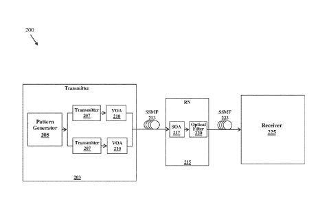
[0037] FIG. 2A is a schematic diagram of a data communications system 200.
The data
communications system 200 is described in Xin Yin, et al., "A 10Gb/s APD-based
linear burst-
mode receiver with 31dB dynamic range for reach-extended PON systems," Optics
Express, vol.
20, no. 26, December 3, 2012. The data communications system 200 generally
comprises a
transmitter 203; SSMFs 213, 223; an RN 215; and a receiver 225. The
transmitter 203 may be
7
CA 3046714 2020-02-11
implemented in the OLT 110 and the receiver 225 may be implemented in one of
the ONUs 120
or vice versa, and the SSMFs 213, 223 and the RN 215 may be implemented in the
ODN 130.
[0038] The transmitter 203 comprises a pattern generator 205, transmitters
207, and VOAs
210. The pattern generator 205 generates optical signals of certain patterns
and provides optical
signals of a first pattern to a first transmitter 207 and optical signals of a
second pattern to a second
transmitter 207. The transmitters 207 transmit the optical signals to the VOAs
210. The VOAs
210 amplify the optical signals and transmit the optical signals to the RN 215
via the SSMF 213.
[0039] The RN 215 comprises a SOA 217 and an optical filter 220. The SOA
217 amplifies
the optical signals. The optical filter 220 selectively modifies the optical
signals to achieve optimal
signal properties for high transmission performance and transmits the optical
signals to the receiver
225 via the SSMF 223. The receiver 225 performs channel equalization on the
optical signals.
The receiver 225 is described further below with respect to FIG. 2B.
[0040] FIG. 2B is a schematic diagram of the receiver 225 in FIG. 2A. The
receiver 225
comprises a VOA 227, an APD linear BM RX 230, a VGA 233, a processor 235, an
FFE 237, a
summation component 240, a CDR component 243, a DFE 245, a phase component
247, an offset
component 250, an error counter 253, and a BER analyzer 255. As mentioned
above, the receiver
225 receives the optical signals from the RN 215 via the SSMF 223. The VOA 227
lowers the
optical signal strength in order to match a desirable receiving quality. The
APD linear BM RX
230 converts the optical signals into electrical signals. The VGA 233
amplifies and samples the
electrical signals to generate burst digital signals. The FFE 237 performs a
linear equalization on
the burst digital signals to generate linear equalized signals.
[0041] The summation component 240 sums a linear equalized signal from the
FFE 237 and a
DFE signal from the DFE 245 to form a summed equalized signal. The summation
component
240 repeatedly performs the summation until channel equalization is completed,
which means
when a sampling phase is optimized and the summed equalized signal is
converged. The CDR
component 243 performs CDR to generate a recovered signal. The DFE 245
performs estimation
on the recovered signal to generate the DFE signal.
[0042] The phase component 247 aligns the recovered signal's phase with the
clock during
channel equalization. The offset component 250 adjusts the signals to offset
loss. The error
counter 253 calculates error data based on the DFE signal, values from the
phase component 247,
and values from the offset component 250. The BER analyzer 255 performs
analyses on the DFE
8
CA 3046714 2020-02-11
signal to determine a number of bit errors. The equalization and the CDR are
performed
continuously until the signals converge and the sampling phase is optimized.
The processor 235
determines when the equalization on the optical signals is completed. As
shown, to guarantee
performance of the receiver 225, the CDR component 243, the FFE 237, and the
DFE 245 are
independent from each other, but that increases complexity, cost, convergence
time, and the
sensitivity of the receiver 225 to ISI.
[0043] FIG. 3 is a graph 300 illustrating a two-level equalization error in
the FFE 237 in FIG.
2B. Specifically, the graph 300 demonstrates experimental results for a 25
Gb/s PON employing
NRZ modulation using a 10 Gb/s EML and APD. The graph 300 includes a sub-graph
310 that is
a magnified portion of the graph 300 as indicated by an arrow. The x-axis
represents a symbol
number in constant units, and the y-axis represents an MSE in dB. Convergence
occurs when a
curve 320 flattens out, which occurs at 51,911 symbols after 2.07 4s, which is
a relatively long
time for channel equalization. After convergence, the MSE is about -8 dB.
[0044] FIG. 4 is a table 400 illustrating a two-level converging time for
different clock phase
errors for the FFE 237 in FIG. 2B. To comprehensively estimate a CDR
converging time, data
with different initial sampling phases is captured and processed. Thus, the
table 400 further
illustrates that a phase error affects the convergence times shown in FIG. 3.
The table 400
comprises three sets of values, a phase error in constant ui, a first
converging time in bits and a
second converging time measure in ns. As shown, the maximum CDR converging
time of 51,911
symbols and 2.07 [Ls (2.0764x10³ns) appears at the sampling point with zero ui
phase error.
[0045] FIG. 5 is a graph 500 illustrating a four-level equalization error
in the FFE 237 in FIG.
2B. Specifically, the graph 500 demonstrates experimental results for a 50
Gb/s PON employing
25 GBd PAM4 modulation using a 10 Gb/s EML and APD. The graph 500 includes a
sub-graph
510 that is a magnified portion of the graph 500 as indicated by an arrow. The
x-axis represents a
symbol number in constant units, and the y-axis represents an MSE in dB.
Convergence occurs
when a curve 520 flattens out, which occurs at 7,537 symbols after 301.48 ns.
After convergence,
the MSE is about -5 dB.
[0046] FIG. 6 is a table 600 illustrating a four-level converging time for
different clock phase
errors for the FFE 237 in FIG. 2B. The table 600 further illustrates that a
phase error affects the
convergence times shown in FIG. 5. The table 600 comprises three sets of
values, a phase error in
constant unit interval (ui), a first converging time in bits, and a second
converging time in ns. As
9
CA 3046714 2020-02-11
=
shown, the maximum CDR converging time of 9,836 symbols and 393.44 ns appears
at the
sampling point with 5/16 ui phase error.
[0047] As demand for faster and increased data transmission rises,
processing and equalization
of that data must also be faster. Especially when development speeds of low-
cost, high-bandwidth
electrical components is not as fast as the increase of PON data rates,
bandwidth restrictions will
introduce severe ISI. In that situation, channel equalization approaches such
as the two-level and
four-level equalization shown above may not be fast enough. It is therefore
desirable to implement
an equalization approach that achieves convergence with fewer symbols while
maintaining or
decreasing an MSE. Such an approach should also reduce system complexity and
ISI sensitivity.
[0048] Disclosed herein are embodiments for higher-level CDR in PONs. The
embodiments
comprise a single FFE, which may be referred to as a fractional FFE because it
performs at least
two functions, namely CDR for phase adjustment and equalization for ISI
compensation. The FFE
is adaptive so that it can track frequency offset and jitter. For those
reasons, the FFE reduces ADC
and DSP complexity. In addition, the FFE implements higher-level CDR, for
instance three-level
CDR for NRZ signals and seven-level CDR for PAM4 signals. The higher-level CDR
shortens a
CDR convergence time, which allows for low-cost, narrow-bandwidth options;
ensures
satisfaction of conversion times required in various PON standards; and
reduces equalization
noise. The embodiments apply to both downstream receivers such as ONUs and
upstream
receivers such as OLTs, though upstream receivers receiving burst-mode signals
may appreciate
the most benefit. Those burst-mode signals may be up to at least 40 Gb/s.
[0049] FIG. 7 is a schematic diagram of a receiver 700 according to an
embodiment of the
disclosure. The receiver 700 may be implemented in the OLT and the ONUs 120,
and the receiver
700 may implement the receiver 225. The receiver 700 comprises a PD 710, a TIA
715, a VCO
720, an ADC 725, a CDR sub-system 730, a PR-MLSE component 755, and a decoder
760.
[0050] The PD 710 converts a burst-mode optical signal into an electric
current signal. The
TIA 715 converts the electric current signal into an amplified voltage signal.
The ADC 725
samples the amplified voltage signal and converts the amplified voltage
signal, which is an analog
electrical signal, to a digital electrical signal. The VCO 720 samples the ADC
725 to synchronize
a frequency between the receiver 700 and a transmitter. However, the receiver
700 and the
transmitter may operate at different phases, which may be referred to as phase
error. Phase error
and ISI are shown in FIG. 8.
CA 3046714 2020-02-11
[0051] FIG. 8 is a graph 800 illustrating phase error and ISI. The x-axis
represents time in
constant units, and the y-axis represents signal amplitude in constant units.
The graph 800
comprises a curve 810 representing a sampled signal, for instance a sampled
signal from the ADC
725, that is sampled at six sampling points, X1 , X2, X3, X4, X5, X6. The
sample points should
be at the middle signal amplitude of each peak in the amplified voltage
signal. However, due to
imperfections in a channel such as the SSMFs 213, 223, the sample points may
not be. First, there
may be phase error so that the ADC samples the simplified voltage signal at
the wrong points.
Thus, the measured center point 820 between sample points X3 and X4 is to the
left of the actual
center point 830 between sample points X3 and X4. In addition, ISI may distort
the peaks of the
curve 810. Thus, the third peak is widened on the left side so that the sample
point X5 is lower
than the middle signal amplitude of the third peak 840.
[0052] Returning to FIG. 7, the CDR sub-system 730 comprises a tap weight
updater 735, an
FFE 740, an error threshold comparator 742, an error calculator 744, a
subtractor 745, and a
decision component 750, which together form a feedback loop to perform CDR and
equalization
and thus compensate for the phase error and ISI described above. Specifically,
in a first iteration,
the FFE 740 passes to the subtractor 745 an equalized signal X", which is the
sampled signal from
the ADC 725 for the first iteration. The decision component 750 passes to the
subtractor 745
decision datum D, which is a training sequence for the first iteration. The
subtractor 745 calculates
an error signal E as follows:
E = )(eq. - D
(1)
The subtractor 745 passes the error signal to the tap weight updater 735 and
the error calculator.
Based on the error signal, the tap weight updater 735 calculates tap weights
W(1), W(2), W(3),
W(4), W(5), W(6) corresponding to the sampling points X1 , X2, X3, X4, X5, X6,
respectively.
[0053] In subsequent iterations, the FFE 740 calculates the equalized
signal as follows:
X" W(1)X(1) + W(2)X(2) + W(3)X(3) + W(4)X(4) + W(5)X(5) + W(6)X(6)
(2)
where X(1), X(2), X(3), X(4), X(5), X(6) correspond to amplitudes of the
sampled signal at the
sampling points X1 , X2, X3, X4, X5, X6, respectively. The FFE 740 passes the
equalized signal
to the subtractor 745 and the decision component 750. As shown below in FIGS.
10A 11A, under
the severe ISI introduced by the restriction of optical devices, the received
signal is overlapped in
11
CA 3046714 2020-02-11
=
the time domain bit by bit and is more like a higher-level signal, for
instance a three-level signal
for NRZ and a seven-level signal for PAM-4, rather than the transmitted two-
level NRZ signal or
four-level PAM-4 signal. Therefore, it is easier to obtain convergence if the
decision component
750 determines the decision datum based on the following higher-level decision
principle:
{6 if Xeq > 5
{4 if Xeq > 3
{2 if Xeq > 1
D = {0 if -1 < Xeq < 1
(3)
{-2 if Xeq < -1
{-4 if Xeg < -3
{-6 if Xeq < -5
The subtractor 745 calculates the error signal using equation (1), the tap
weight updater 735
calculates the tap weights based on the error signal, and the FFE 740 again
calculates the equalized
signal using equation (2).
[0054] That feedback loop continues until the equalized signal converges
and therefore has an
equalization error at or below a predetermined threshold. Specifically, the
error calculator 744
calculates the MSE of the equalization error. The error threshold comparator
742 determines
whether the MSE is less than the threshold. If the error is equal to or less
than the threshold, then
the error threshold comparator 742 instructs the CDR sub-system 730 to
discontinue the feedback
loop. If the error is greater than the threshold, then the error threshold
comparator 742 provides
no instruction to the CDR sub-system 730 or instructs the CDR sub-system 730
to continue the
feedback loop. The threshold is, for instance, -6 dB.
[0055] Though six tap weights, sampling points, and amplitudes are
described, the CDR sub-
system 730 may employ any suitable number of tap weights, sampling points, and
amplitudes. In
addition, the decision datum is a three-level decision datum applicable to,
for instance, two-level
NRZ signals. Similarly, the decision datum may be seven-level decision datum
applicable to, for
instance, PAM4 signals. Regardless of the level of the incoming signal, the
CDR sub-system 730
may implement higher-level decision datum. Furthermore, though a threshold is
described for
determining convergence, the CDR sub-system 730 may implement any suitable
indicator of
convergence.
[0056] The tap weight updater 735 notifies the FFE 740 that the equalized
signal is converged.
Thereafter, the FFE 740 passes the equalized signal to the PR-MLSE component
755. The PR-
12
CA 3046714 2020-02-11
MLSE component 755 uses the known channel response to map the binary decision
bit into higher-
level bits through a summation of a former and a latter bit at individual time
instances. The
combinations of different possible decision bits form different trellis paths
The PR-MLSE
component 755 uses the path with a lowest Euclid distance compared to the
equalized signal after
the FFE 740 to be the most reliable bit path. The PR-MLSE component 755
outputs bits on the
most reliable path and de-maps those bits into a binary signal. Through the
above steps, the PR-
MLSE component 755 performs an MLSE on the equalized signal to convert the
equalized signal
to an estimated signal, which is a binary, two-level signal. The decoder 760
decodes the estimated
signal to generate a decoded signal for further processing.
[0057] FIG. 9 is a schematic diagram of a device 900 according to an
embodiment of the
disclosure. The device 900 may implement the disclosed embodiments, for
instance the receiver
700. The device 900 comprises ingress ports 910 and an RX 920 for receiving
data; a processor,
logic unit, or CPU 930 to process the data; a TX 940 and egress ports 950 for
transmitting the data;
and a memory 960 for storing the data. The device 900 may also comprise OE
components and
EO components coupled to the ingress ports 910, the RX 920, the TX 940, and
the egress ports
950 for ingress or egress of optical or electrical signals.
[0058] The processor 930 is implemented by any suitable combination of
hardware,
middleware, firmware, and software. The processor 930 may be implemented as
one or more CPU
chips, cores (e.g., as a multi-core processor), FPGAs, ASICs, or DSPs. The
processor 930 is in
communication with the ingress ports 910, RX 920, TX 940, egress ports 950,
and memory 960.
The processor 930 comprises a CDR component 970, which may implement the
disclosed
embodiments. The inclusion of the CDR component 970 therefore provides a
substantial
improvement to functionality of the device 900 and effects a transformation of
the device 900 to a
different state. Alternatively, the memory 960 stores the CDR component 970 as
instructions, and
the processor 930 executes those instructions.
[0059] The memory 960 comprises one or more disks, tape drives, or solid-
state drives and
may be used as an over-flow data storage device, to store programs when such
programs are
selected for execution, or to store instructions and data that are read during
program execution.
The memory 960 may be volatile or non-volatile and may be any combination of
ROM, RAM,
TCAM, or SRAM.
13
CA 3046714 2020-02-11
=
[0060] In an example embodiment, the device 900 includes an electrical
conversion module
converting an optical signal with a first modulation format to an analog
electrical signal, a
digitization module converting the analog electrical signal to a first digital
signal, an equalization
module equalizing the first digital signal into a second digital signal with a
second modulation
format, wherein the second modulation format has more levels than the first
modulation format,
and a recovery module performing clock and data recovery (CDR) on the second
digital signal. In
some embodiments, the device 900 may include other or additional modules for
performing any one
of or combination of steps described in the embodiments. Further, any of the
additional or alternative
embodiments or aspects of the method, as shown in any of the figures or
recited in any of the claims,
are also contemplated to include similar modules.
[0061] FIG. 10A is a diagram 1000 illustrating a two-level NRZ signal prior
to three-level
CDR. The x-axis represents time or symbol duration in constant units, and the
y-axis represents
amplitude in constant units. As can be seen, the two-level NRZ signal appears
to have almost
three levels and is not well defined due to ISI.
[0062] FIG. 10B is a graph 1010 illustrating a three-level NRZ signal after
higher-level CDR
according to an embodiment of the disclosure. The x-axis represents time in
seconds, and the y-
axis represents amplitude in constant units. As shown, the higher-level CDR
substantially
eliminates ISI to produce a well-defined, three-level NRZ signal unlike the
two-level NRZ signal
in FIG. 10A.
[0063] FIG. 11A is a diagram 1100 illustrating a four-level PAM4 signal
prior to seven-level
CDR. The x-axis represents time in seconds, and the y-axis represents
amplitude in constant units.
As can be seen, the four-level PAM4 signal appears to have almost seven levels
and is not well
defined due to ISI.
[0064] FIG. 11B is a graph 1110 illustrating a seven-level PAM4 signal
after higher-level CDR
according to an embodiment of the disclosure. The x-axis represents time in
seconds, and the y-
axis represents amplitude in constant units. As shown, the higher-level CDR
substantially
eliminates ISI to produce a well-defined, seven-level signal unlike the four-
level PAM4 signal in
FIG. 11A.
[0065] FIG. 12 is a graph 1200 illustrating an equalization error for the
FFE 740 in FIG. 7
equalizing a two-level NRZ signal using three-level equalization according to
an embodiment of
the disclosure. The graph 1200 comprises a sub-graph 1210 that is a magnified
portion of the
14
CA 3046714 2020-02-11
graph 1200 as indicated by an arrow. The x-axis represents a symbol number in
constant units,
and the y-axis represents an MSE in dB. Convergence occurs when a curve 1220
flattens out,
which occurs at about 2,789 symbols after 111.56 ns. After convergence, the
MSE is about -9 dB,
which is about 2 dB lower than that shown in FIG. 3
[0066] FIG. 13 is a table 1300 illustrating a converging time for the FFE
740 in FIG. 7
equalizing a two-level NRZ signal using three-level equalization according to
an embodiment of
the disclosure. The table 1300 further illustrates the convergence time shown
in FIG. 12. The
table 1300 comprises three sets of values, a phase error in ui, a first
converging time in bits, and a
second converging time in ns. As shown, there is no phase error at the
converging point of 2,789
symbols and 111.56 ns. The maximum CDR converging time of 4,048 symbols and
161.92 ns
appears at the sampling point with 3/16 ui phase error.
[0067] FIG. 14 is a graph 1400 illustrating an equalization error for the
FFE 740 in FIG. 7
equalizing a four-level PAM4 signal using seven-level equalization according
to an embodiment
of the disclosure. The graph 1400 comprises a sub-graph 1410 that is a
magnified portion of the
graph 1400 as indicated by an arrow. The x-axis represents a symbol number in
constant units,
and the y-axis represents an MSE in dB. Convergence occurs when a curve 1420
flattens out,
which occurs at about 2,936 symbols after 117.44 ns. After convergence, the
MSE is about -12
dB, which is about 7 dB lower than that shown in FIG. 5
[0068] FIG. 15 is a table 1500 illustrating a converging time for the FFE
740 in FIG. 7
equalizing a four-level PAM4 signal using seven-level equalization according
to an embodiment
of the disclosure. The table 1500 further illustrates the convergence time
shown in FIG. 14. The
table 1500 comprises three sets of values, a phase error in ui, a first
converging time in bits, and a
second converging time in ns. As shown, the maximum CDR converging time of
2,783 symbols
and 111.72 ns appears at the sampling point with 6/16 ui phase error.
[0069] In comparing FIGS. 3-4 to FIGS. 12-13, the higher-level CDR reduces
a convergence
time for two-level NRZ signals from 51,911 symbols after 2.07 trs to 2,789
symbols after 111.56
ns. In other words, the higher-level CDR converges at least 18.5 times
quicker. In comparing
FIGS. 5-6 to FIGS. 14-15, the higher-level CDR reduces a convergence time for
four-level PAM4
signals from 7,537 symbols after 301.48 ns to 2,936 symbols after 117.44 ns.
In other words, the
higher-level CDR converges at least 2.5 times quicker.
CA 3046714 2020-02-11
=
[0070] FIG. 16 is a flowchart of a method 1600 of performing higher-level
CDR according to
an embodiment of the disclosure. The receiver 700 performs the method 1600. At
step 1610, a
signal is received. For instance, the PD 710 receives an optical signal. At
step 1620, the signal is
equalized using higher-level CDR. For instance, after the PD 710, TIA 715, and
ADC 725 convert
the optical signal into a digital signal, the CDR sub-system 730 performs CDR,
including FFE, as
described above. In the meantime, the CDR sub-system 730 adaptively updates
the tap weights.
As a first example, the CDR sub-system 730 performs CDR of a two-level NRZ
signal using three-
level equalization. As a second example, the CDR sub-system 730 performs CDR
of a four-level
PAM4 signal using seven-level equalization. At step 1630, an MSE is
calculated. For instance,
the error calculator 744 calculates the MSE of the equalization error. At
decision diamond 1640,
it is determined whether the MSE is less than a threshold. For instance, the
error threshold
comparator 742 determines whether the MSE is less than the threshold described
above. If it is
not, then the method 1600 returns to step 1630. If it is, then the method 1600
proceeds to step
1650. Finally, at step 1650, PR-MLSE and decoding are performed. For instance,
the PR-MLSE
component 755 performs PR-MLSE and the decoder 760 performs decoding.
100711 FIG. 17 is a flowchart of a method 1700 of performing higher-level
CDR according to
another embodiment of the disclosure. The receiver 700 performs the method
1700. At step 1710,
an optical signal with a first modulation format is converted to an analog
electrical signal. For
instance, the PD 710 converts the optical signal into an electric current
signal, and the TIA 715
converts the electric current signal into an amplified voltage signal, which
is an analog electrical
signal. At step 1720, the analog electrical signal is converted to a first
digital signal. For instance,
the ADC 725 converts that analog electrical signal to a first digital signal
at the first level. At step
1730, the first digital signal is equalized into a second digital signal with
a second modulation
format. For instance, the CDR sub-systeni 730 equalizes the first digital
signal into the second
digital signal at the second level. The second modulation format has more
levels than the first
modulation format. Finally, at step 1740, CDR is performed on the second
digital signal. For
instance, the CDR sub-system 730 performs CDR on the second digital signal.
100721 In an example embodiment, an apparatus comprises: an OE element
configured to
convert an optical signal with a first modulation format to an analog
electrical signal; an ADC
element coupled to the OE element and configured to convert the analog
electrical signal to a first
digital signal; and a CDR element coupled to the OE element and configured to:
equalize the first
16
CA 3046714 2020-02-11
digital signal into a second digital signal with a second modulation format,
wherein the second
modulation format has more levels than the first modulation format; and
perform CDR on the
second digital signal.
[0073] A first component is directly coupled to a second component when
there are no
intervening components, except for a line, a trace, or another medium between
the first component
and the second component. The first component is indirectly coupled to the
second component
when there are intervening components other than a line, a trace, or another
medium between the
first component and the second component. The term "coupled" and its variants
include both
directly coupled and indirectly coupled. The use of the term "about" means a
range including
10% of the subsequent number unless otherwise stated.
[0074] While several embodiments have been provided in the present
disclosure, it may be
understood that the disclosed systems and methods might be embodied in many
other specific
forms without departing from the spirit or scope of the present disclosure.
The present examples
are to be considered as illustrative and not restrictive, and the intention is
not to be limited to the
details given herein. For example, the various elements or components may be
combined or
integrated in another system or certain features may be omitted, or not
implemented.
[0075] In addition, techniques, systems, subsystems, and methods described
and illustrated in
the various embodiments as discrete or separate may be combined or integrated
with other systems,
units, techniques, or methods without departing from the scope of the present
disclosure. Other
items shown or discussed as coupled or directly coupled or communicating with
each other may
be indirectly coupled or communicating through some interface, device, or
intermediate
component whether electrically, mechanically, or otherwise. Other examples of
changes,
substitutions, and alterations are ascertainable by one skilled in the art and
may be made without
departing from the spirit and scope disclosed herein.
17
CA 3046714 2020-02-11