Note: Descriptions are shown in the official language in which they were submitted.
LOW-POWER SMART CARD READER
FIELD OF THE INVENTION
The present invention relates generally to a power-on sequence for a smart
card
reader.
BACKGROUND OF THE INVENTION
Today, small and medium sized businesses (SMBs) often use mobile point-of-sale
(mPOS) devices to perform transactions and accept payments such as from credit
cards,
debit cards, mobile wallets, etc. For example, an SMB may utilize a reader
device that
communicates with a host device such as a smartphone or tablet computer. The
reader
device may include a magnetic stripe reader (MSR) for accepting various types
of
magnetic stripe cards, a chip reader for accepting so-called smart cards
(e.g., Europay
MasterCard Visa or EMV cards), a contactless reader (e.g., a near-field
communications
or NFC reader for accepting various types of contactless payment vehicles such
as Apple
Pay), and/or other types of readers such as, for example, a camera or scanner
such as for
reading a bar-code or QR-code. The reader device may communicate with the host
device such as by USB, Bluetooth, audio jack, lightning, Wi-Fi, infrared,
cellular, or
other communication technology.
In the early days of mPOS for SMB in the US market, solutions were mostly
based on magnetic stripe readers having ultra-low power microcontrollers and
connected
to the host device by the audio jack. Many such reader devices relied on power
from the
host device (e.g., in the form of audio signals or other power signals
provided by the host
-1-
Date Recue/Date Received 2021-01-14
device allowing the reader device to charge a capacitor or other electrical
storage device
such as a battery) or from a non-rechargeable battery allowing hundreds or
thousands of
transactions over several years. As a major benefit for the merchants, the
reader devices
were ready for use without having to worry about charging the reader devices.
With the introduction of EMV capability, it is not practical for reader
devices to
rely on power from the host device or from a non-rechargeable battery because
these
devices consume a great deal of power. Therefore, EMV-capable reader devices
typically include a rechargeable battery such as a rechargeable Li-Ion
battery. Beyond
the self-discharge of such technology, the lifecycle of a transaction
exacerbates high
power consumption of these reader devices. For example, a typical transaction
lifecycle
for the card reader includes running a start-up sequence typically including
communications with the host device, idling while awaiting card insertion,
reading
information from the card when it is inserted, processing the transaction once
the card
was inserted including communications with the host device, and waiting for
transaction
completion on the back-end to be returned to the card reader. In order to
control power
consumption by such card readers, it is common for the card reader to include
a power-on
button or other mechanism to turn on the card reader in advance of the
transaction and for
the card reader to be turned off after completion of the transaction. Still,
it is not
uncommon for SMB merchants (especially those that do not perform frequent
transactions) to find that their card readers are not sufficiently charged to
accept
transactions, thereby requiring that the SMB merchant charge the reader device
for
several minutes at a time when they want to accept payments.
In order to enable faster transactions, all of the major card brands (e.g.,
Visa,
MasterCard, American Express, and Discover) have introduced a "Quick Chip" or
similar
online transaction mode that allows the card to be inserted, read, and removed
without the
need for the final transaction amount to be available in advance and without
the need for
the card reader to receive approval from the back-end before instructing the
customer to
remove the card.
-2-
CA 3046748 2019-06-17
BRIEF DESCRIPTION OF THE DRAWINGS
The foregoing features of embodiments will be more readily understood by
reference to the following detailed description, taken with reference to the
accompanying
drawings, in which:
FIG. 1 is a schematic block diagram of a reader device 100 in which power-on
is
initiated by a manual power switch, as known in the art.
FIG. 2 is a schematic diagram showing relevant components of an exemplary IC
slot 108 that can be used in the reader device 100 of FIG. 1, as known in the
art.
FIG. 3 is a schematic diagram showing relevant components of an exemplary
manual power switch circuit 104 that can be used in the reader device 100 of
FIG. 1, as
known in the art.
FIG. 4 is a schematic block diagram of a reader device 200 in which power-on
is
initiated by insertion of a card in the IC slot, in accordance with a first
exemplary
embodiment.
FIG. 5 is a schematic diagram showing one example of an electronic power
switch circuit 204 that can be used in various embodiments of the invention.
FIG. 6 is a schematic block diagram of a reader device 300 in which power-on
requires both insertion of a card in the IC slot and connection of the reader
device 300 to
the host device, in accordance with a second exemplary embodiment.
FIG. 7 is a schematic block diagram of a reader device 400 in which power-on
requires operation of a manual power switch while a card is inserted in the IC
slot, in
accordance with a third exemplary embodiment.
FIG. 8 is a schematic block diagram of a reader device 500 in which power-on
requires operation of a manual power switch while a card is inserted in the IC
slot and the
reader device is connected to the host device, in accordance with a fourth
exemplary
embodiment.
It should be noted that the foregoing figures and the elements depicted
therein are
not necessarily drawn to consistent scale or to any scale. Unless the context
otherwise
suggests, like elements are indicated by like numerals.
-3-
CA 3046748 2019-06-17
DETAILED DESCRIPTION OF SPECIFIC EMBODIMENTS
In exemplary embodiments, a reader device is powered on only when a card is
inserted in the reader device, thereby reducing the amount of time the reader
device is
powered and consequently reducing the amount of power consumption by the
reader
device. In some embodiments, inserting the card causes power-on of the reader
device,
while in other embodiments, insertion of the card plus other criteria are
required to power
on the reader device (e.g., having the reader device connected to the host
device, or
operating a manual switch while the card is inserted in the reader device).
FIG. 1 is a schematic block diagram of a reader device 100 in which power-on
is
initiated by a manual power switch, as known in the art. Among other things,
the reader
device 100 includes a battery 102 or other power source, a manual power switch
circuit
104, a processing system 106, and an IC slot 108.
FIG. 2 is a schematic diagram showing relevant components of an exemplary IC
slot 108 that can be used in the reader device 100 of FIG. 1, as known in the
art. Here,
the IC slot 108 includes a set of eight (8) card interface pins 1081 that are
configured to
interface with corresponding pins of the smart card chip when the smart card
is inserted
in the IC slot 108 (the arrow shows the direction of card insertion). The card
interface
pins also are coupled to the processing system 106 via the DATA interface so
that the
processing system 106 can read card data from the smart card chip. The IC slot
108 also
includes a card detection device 1082, which in this example is a normally-
open switch
that is closed when the smart card is inserted in the IC slot 108. The card
detection
device 1082 provides a signal 109 that essentially indicates whether or not a
card is
inserted in the IC slot 108, e.g., based on whether the card detection switch
is open (i.e.,
no card inserted, signal 109 = 0) or closed (i.e., card inserted, signal 109 =
VCC). The
card interface pins 1081 and the card detection device 1082 may be parts of an
integrated
card connector component or may be separate components, e.g., attached
separately to a
printed circuit board. The IC slot 108 typically also includes guides (not
shown) that help
-4-
CA 3046748 2019-06-17
to position the smart card within the IC slot 108 when the smart card is
inserted in the IC
slot 108.
FIG. 3 is a schematic diagram showing relevant components of an exemplary
manual power switch circuit 104 that can be used in the reader device 100 of
FIG. 1, as
known in the art. Here, the manual power switch circuit 104 includes, among
other
things, a momentary normally-open push-button switch (Si) and additional power
management circuitry that is controlled by the processing system 106 or other
appropriate
circuitry to maintain power for the processing system 106 and other
peripherals (e.g., the
IC slot 108). When the switch Si is pressed/closed, current flows through
resistor R1
and through the diode to the control input of transistor Ql to provide a POWER-
ON
signal to the processing system 106. Upon receiving the POWER-ON signal, the
processing system 106 or other appropriate circuitry provides a CONTROL signal
to the
control input of transistor Q1 to maintain the POWER-ON signal even if the
switch (S
is subsequently released/opened. Typically, the processing system 106 can turn
off the
reader device by turning off the CONTROL signal. For example, the CONTROL
signal
may be a software-controllable output pin of a microcontroller of the
processing system
106, in which case the reader device can be turned off by software control.
Thus, with reference to FIGs. 1-3, the user of the reader device 100 can
operate
the manual power switch circuit 104 to provide a POWER-ON signal to the
processing
system 106. Then, with regard to smart card transaction, the processing system
106 can
determine, based on the signal 109, whether or not a card is inserted in the
IC slot 108.
When a card is inserted in the IC slot 108, the processing system 106 can read
data from
the card and can transmit card data to the host device via a host interface
(not shown), if
the reader device 100 is connected to the host device, or in some embodiments
can store
the card data in a memory of the processing system 106 for later transmission
to the host
device. The processing system 106 also can detect when the card has been
removed from
the IC slot 108.
-5-
CA 3046748 2019-06-17
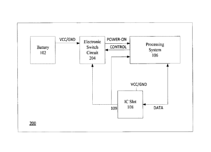
FIG. 4 is a schematic block diagram of a reader device 200 in which power-on
is
initiated by insertion of a card in the IC slot, in accordance with a first
exemplary
embodiment. Here, power is provided to the normally-open card detection device
1082
of the IC slot 108 such that, when a card is inserted in IC slot 108 and the
card detection
device 1082 is closed, signal 109 is generated to operate electronic power
switch 204 and
provide a power-on signal to the processing system 106. In essence, the signal
109
replaces the momentary normally-open push-button switch (Si) of the manual
power
switch circuit 104 of FIG. 3, for example, as shown in FIG. 5. Then, the
processing
system 106 can determine, based on the signal 109, whether or not a card is
inserted in
the IC slot 108. When a card is inserted in the IC slot 108, the processing
system 106 can
read data from the card and can transmit card data to the host device via a
host interface
(not shown), if the reader device 200 is connected to the host device, or in
some
embodiments can store the card data in a memory of the processing system 106
for later
transmission to the host device, e.g., if the card reader is not connected to
the host device
or the host device is not ready to receive the card data.
FIG. 6 is a schematic block diagram of a reader device 300 in which power-on
requires both insertion of a card in the IC slot and connection of the reader
device 300 to
the host device, in accordance with a second exemplary embodiment. here, as in
FIG. 4,
power is provided to the normally-open card detection device 1082 of the IC
slot 108
such that, when a card is inserted in IC slot 108 and the card detection
device is closed,
signal 109 is generated. Separately, the host device can provide a signal 309
when the
reader device is connected to the host device via host interface 310 (e.g.,
through the
audio jack, lightning jack for iOS devices, USB, etc.). For example, host
device may
provide a signal when it is ready to receive card data from the reader device
300 (e.g.,
sent automatically by a transaction app on the host device when the
transaction app is
open and waiting to receive the data from reader device). Signals 109 and 309
are
provided to an AND circuit 312. When both signals 109 and 309 are present,
signal 609
is generated to operate electronic power switch 204 and provide a power-on
signal to the
processing system 106. In essence, the signal 609 replaces the momentary
normally-open
push-button switch (Si) of the manual power switch circuit 104 of FIG. 3, for
example,
-6-
CA 3046748 2019-06-17
as shown in FIG. 5. Then, the processing system 106 can determine, based on
the signal
109, whether or not a card is inserted in the IC slot 108. When a card is
inserted in the IC
slot 108, the processing system 106 can read data from the card and can
transmit card
data to the host device via a host interface (not shown), if the reader device
300 is
connected to the host device, or in some embodiments can store the card data
in a
memory of the processing system 106 for later transmission to the host device,
e.g., if the
card reader is not connected to the host device or the host device is not
ready to receive
the card data.
FIG. 7 is a schematic block diagram of a reader device 400 in which power-on
requires operation of a manual power switch while a card is inserted in the IC
slot, in
accordance with a third exemplary embodiment. Here, as in FIG. 2, power is
provided to
the normally-open card detection device of the IC slot 108 such that, when a
card is
inserted in IC slot 108 and the card detection device is closed, signal 109 is
generated.
Separately, manual power switch 410 provides signal 409 when the user operates
the
manual power switch 410. Signals 109 and 409 are provided to an AND circuit
312.
When both signals 109 and 409 are present, signal 709 is generated to operate
electronic
power switch 204 and provide a power-on signal to the processing system 106.
In
essence, the signal 709 replaces the momentary normally-open push-button
switch (Si)
of the manual power switch circuit 104 of FIG. 3, for example, as shown in
FIG. 5.
Then, the processing system 106 can determine, based on the signal 109,
whether or not a
card is inserted in the IC slot 108. When a card is inserted in the IC slot
108, the
processing system 106 can read data from the card and can transmit card data
to the host
device via a host interface (not shown), if the reader device 400 is connected
to the host
device, or in some embodiments can store the card data in a memory of the
processing
system 106 for later transmission to the host device, e.g., if the card reader
is not
connected to the host device or the host device is not ready to receive the
card data.
FIG. 8 is a schematic block diagram of a reader device 500 in which power-on
requires operation of a manual power switch while a card is inserted in the IC
slot and the
reader device is connected to the host device, in accordance with a fourth
exemplary
-7-
CA 3046748 2019-06-17
embodiment. Here, as in FIG. 2, power is provided to the normally-open card
detection
device of the IC slot 108 such that, when a card is inserted in IC slot 108
and the card
detection device is closed, signal 109 is generated. Separately, the host
device can
provide a signal 309 when the reader device is connected to the host device
via host
interface 310 (e.g., through the audio jack, lightning jack for iOS devices,
USB, etc.).
For example, host device may provide a signal when it is ready to receive card
data from
the reader device 500. Separately, manual power switch 410 provides signal 409
when
the user operates the manual power switch 410. Signals 109, 309, and 409 are
provided
to an AND circuit 312. When all three signals 109, 309, and 409 are present,
signal 809
is generated to operate electronic power switch 204 and provide a power-on
signal to the
processing system 106. In essence, the signal 809 replaces the momentary
normally-open
push-button switch (Si) of the manual power switch circuit 104 of FIG. 3, for
example,
as shown in FIG. 5. Then, the processing system 106 can determine, based on
the signal
109, whether or not a card is inserted in the IC slot 108. When a card is
inserted in the IC
slot 108, the processing system 106 can read data from the card and can
transmit card
data to the host device via a host interface (not shown), if the reader device
400 is
connected to the host device, or in some embodiments can store the card data
in a
memory of the processing system 106 for later transmission to the host device,
e.g., if the
card reader is not connected to the host device or the host device is not
ready to receive
the card data.
It should be noted that the processing system 106 typically includes a
processor
(e.g., a microprocessor or microcontroller with memory and other peripherals,
and/or
application-specific hardware) configured accordingly to perform device
functions. For
example the processing system 106 is typically configured to read card data
from the card
and process the card data, which may include encrypting the card data and
either storing
the encrypted data or transmitting the encrypted data to the host device along
with
additional data relating to the reader device and/or transaction. In some
embodiments,
the processing system 106 includes other user interface devices (e.g., a
keypad, a display
screen, a touchscreen, etc.) and can be configured to present information to
the user
and/or accept inputs from the user via the user interface devices.
-8-
CA 3046748 2019-06-17
Importantly, the processing system 106 can be configured to turn off the
reader
device after card data has been stored or transmitted to the host device,
e.g., upon
receiving a signal from the host device indicating that the card data has been
successfully
received by the host device (e.g., the host device may send an acknowledgment
to the
reader along with a beep command and a power-off command), or automatically by
the
processing system 106 upon completion of storing card data for later
transmission. It
should be noted that the reader device can be turned off even if the card
remains inserted
in the IC slot 108.
Thus, the reader devices of the types described with reference to FIGs. 4-8
can be
powered on for a minimal amount of time, starting no earlier than insertion of
the card
and powering down after the card data has been read and processed, thereby
providing
improved power savings and reduced transaction times. For example, card data
could be
collected and processed, and the reader powered down, before the host system
is ready to
complete the transaction using the card data. As discussed above, in some
situations
(e.g., when the reader device is not connected to the host device), the card
data may be
stored locally by the reader device for later transmission to the host device.
Typically,
the card data would be stored in encrypted form. Also, the card data may be
stored with a
timestamp and deleted after either being transmitted to the host device or
being stored for
more than a predetermined amount time based on the timestamp.
In some embodiments, the reader device firmware run by the processing system
106 may utilize a "thin" client architecture so as to omit a full operating
system, thereby
providing very fast power-up and initialization of the reader device. It is
expected that
this fast power-up and initialization, together with "quick chip" reading and
processing of
the card data followed by virtually immediate power-down of the reader device,
will
result in a total transaction time below around 8 to 10 seconds (which is
below the typical
time that consumers are experiencing with "non Quick chip" EMV transactions)
and
perhaps could be reduced to under 3 seconds and perhaps under 2 seconds in
some
situations. Together with use of a low-power microcontroller, per-transaction
power
-9-
CA 3046748 2019-06-17
consumption can be very low, thereby significantly extending the time between
recharge
cycles and in some cases making it practical to possibly return to the use of
non-
rechargeable batteries, which can be a substantial cost saving.
Exemplary embodiments described herein should be particularly useful for "chip-
only" reader devices. With the migration of the market to EMV, as of the end
of 2017,
more than 95% of transactions are already EMV (when the reader device is EMV
capable). MSR capabilities are being phased out. For example, Mastercard has
already
released information for the European market that MSR is no longer required in
reader
devices. Also, there currently is no mandate that reader devices support
contactless
reading capabilities. Thus, it becomes possible to consider introducing chip-
only reader
devices, i.e., having only chip-reading capabilities without MSR or
contactless
capabilities that generally require that the reader device be powered on for a
longer
amount of time.
That being said, the present invention is not limited to chip-only reader
devices.
For example, reader devices could include circuitry of the type described
herein that
powers on the reader device when a card is inserted in the IC slot, and the
reader device
also could include other circuitry that powers on the reader device for other
functions
such as MSR or contactless transactions (e.g., a power on switch/button).
Additionally or
alternatively, some reader devices include a slot for MSR transactions, and
power-on
circuitry of the type described herein could be used to power on the reader
device when
the card is inserted in the slot (e.g., the reader device may be powered on
when the card is
inserted, and the user may have to wait until the reader device is operational
and provides
a signal, such as audible or visual signal, for the user to remove the card
and effectuate
the MSR transaction).
It should be noted that embodiments are not limited to any particular type of
reader device or reader device application. Thus, for example, embodiments can
include
reader devices that connect to a host device using any of wide range of
technologies (e.g.,
USB, Bluetooth, audio jack, lightning, Wi-Fi, infrared, cellular, or other
communication
-10-
CA 3046748 2019-06-17
technology). Embodiments can include portable devices or stationary devices.
Embodiments can include reader devices that are used in or with other products
such as
vending machines, appliances (e.g., Laundromat washers and dryers), kiosks,
access/entry systems, etc. The described power-on and/or power-off controls
based on
insertion of the card into the reader device can be used to turn on a device
or device
circuitry to read card data and then power down the device or device circuitry
when
processing is completed, thereby allowing for power savings benefits to be
applied to a
wide range of devices, even devices that are plugged-in rather than battery-
powered.
It should be noted that arrows may be used in drawings to represent
communication, transfer, or other activity involving two or more entities.
Double-ended
arrows generally indicate that activity may occur in both directions (e.g., a
command/request in one direction with a corresponding reply back in the other
direction,
or peer-to-peer communications initiated by either entity), although in some
situations,
activity may not necessarily occur in both directions. Single-ended arrows
generally
indicate activity exclusively or predominantly in one direction, although it
should be
noted that, in certain situations, such directional activity actually may
involve activities in
both directions (e.g., a message from a sender to a receiver and an
acknowledgement
back from the receiver to the sender, or establishment of a connection prior
to a transfer
and termination of the connection following the transfer). Thus, the type of
arrow used in
a particular drawing to represent a particular activity is exemplary and
should not be seen
as limiting.
It should also be noted that devices may use communication protocols and
messages (e.g., messages created, transmitted, received, stored, and/or
processed by the
device), and such messages may be conveyed by a communication network or
medium.
Unless the context otherwise requires, the present invention should not be
construed as
being limited to any particular communication message type, communication
message
format, or communication protocol. Thus, a communication message generally may
include, without limitation, a frame, packet, datagram, user datagram, cell,
or other type
of communication message. Unless the context requires otherwise, references to
specific
-11-
CA 3046748 2019-06-17
communication protocols are exemplary, and it should be understood that
alternative
embodiments may, as appropriate, employ variations of such communication
protocols
(e.g., modifications or extensions of the protocol that may be made from time-
to-time) or
other protocols either known or developed in the future.
It should also be noted that logic flows may be described herein to
demonstrate
various aspects of the invention, and should not be construed to limit the
present
invention to any particular logic flow or logic implementation. The described
logic may
be partitioned into different logic blocks (e.g., programs, modules,
functions, or
subroutines) without changing the overall results or otherwise departing from
the true
scope of the invention. Often times, logic elements may be added, modified,
omitted,
performed in a different order, or implemented using different logic
constructs (e.g., logic
gates, looping primitives, conditional logic, and other logic constructs)
without changing
the overall results or otherwise departing from the true scope of the
invention.
The present invention may be embodied in many different forms, including, but
in
no way limited to, computer program logic for use with a processor (e.g., a
microprocessor, microcontroller, digital signal processor, or general purpose
computer),
programmable logic for use with a programmable logic device (e.g., a Field
Programmable Gate Array (FPGA) or other PLD), discrete components, integrated
circuitry (e.g., an Application Specific Integrated Circuit (ASIC)), or any
other means
including any combination thereof. Computer program logic implementing some or
all
of the described functionality is typically implemented as a set of computer
program
instructions that is converted into a computer executable form, stored as such
in a
computer readable medium, and executed by a microprocessor under the control
of an
operating system. Hardware-based logic implementing some or all of the
described
functionality may be implemented using one or more appropriately configured
FPGAs.
Computer program logic implementing all or part of the functionality
previously
described herein may be embodied in various forms, including, but in no way
limited to,
a source code form, a computer executable form, and various intermediate forms
(e.g.,
-12-
CA 3046748 2019-06-17
forms generated by an assembler, compiler, linker, or locator). Source code
may include
a series of computer program instructions implemented in any of various
programming
languages (e.g., an object code, an assembly language, or a high-level
language such as
Fortran, C, C++, JAVA, or HTML) for use with various operating systems or
operating
environments. The source code may define and use various data structures and
communication messages. The source code may be in a computer executable form
(e.g.,
via an interpreter), or the source code may be converted (e.g., via a
translator, assembler,
or compiler) into a computer executable form.
Computer program logic implementing all or part of the functionality
previously
described herein may be executed at different times on a single processor
(e.g.,
concurrently) or may be executed at the same or different times on multiple
processors
and may run under a single operating system process/thread or under different
operating
system processes/threads. Thus, the term "computer process" refers generally
to the
execution of a set of computer program instructions regardless of whether
different
computer processes are executed on the same or different processors and
regardless of
whether different computer processes run under the same operating system
process/thread
or different operating system processes/threads.
The computer program may be fixed in any form (e.g., source code form,
computer executable form, or an intermediate form) either permanently or
transitorily in
a tangible storage medium, such as a semiconductor memory device (e.g., a RAM,
ROM,
PROM, EEPROM, or Flash-Programmable RAM), a magnetic memory device (e.g., a
diskette or fixed disk), an optical memory device (e.g., a CD-ROM), a PC card
(e.g.,
PCMCIA card), or other memory device. The computer program may be fixed in any
form in a signal that is transmittable to a computer using any of various
communication
technologies, including, but in no way limited to, analog technologies,
digital
technologies, optical technologies, wireless technologies (e.g., Bluetooth),
networking
technologies, and internetworking technologies. The computer program may be
distributed in any form as a removable storage medium with accompanying
printed or
electronic documentation (e.g., shrink wrapped software), preloaded with a
computer
-13-
CA 3046748 2019-06-17
system (e.g., on system ROM or fixed disk), or distributed from a server or
electronic
bulletin board over the communication system (e.g., the Internet or World Wide
Web).
Hardware logic (including programmable logic for use with a programmable logic
device) implementing all or part of the functionality previously described
herein may be
designed using traditional manual methods, or may be designed, captured,
simulated, or
documented electronically using various tools, such as Computer Aided Design
(CAD), a
hardware description language (e.g., VHDL or AHDL), or a PLD programming
language
(e.g., PALASM, ABEL, or CUPL).
Programmable logic may be fixed either permanently or transitorily in a
tangible
storage medium, such as a semiconductor memory device (e.g., a RAM, ROM, PROM,
EEPROM, or Flash-Programmable RAM), a magnetic memory device (e.g., a diskette
or
fixed disk), an optical memory device (e.g., a CD-ROM), or other memory
device. The
programmable logic may be fixed in a signal that is transmittable to a
computer using any
of various communication technologies, including, but in no way limited to,
analog
technologies, digital technologies, optical technologies, wireless
technologies (e.g.,
Bluetooth), networking technologies, and internetworking technologies. The
programmable logic may be distributed as a removable storage medium with
accompanying printed or electronic documentation (e.g., shrink wrapped
software),
preloaded with a computer system (e.g., on system ROM or fixed disk), or
distributed
from a server or electronic bulletin board over the communication system
(e.g., the
Internet or World Wide Web). Of course, some embodiments of the invention may
be
implemented as a combination of both software (e.g., a computer program
product) and
hardware. Still other embodiments of the invention are implemented as entirely
hardware, or entirely software.
Importantly, it should be noted that embodiments of the present invention may
employ conventional components such as conventional computers (e.g., off-the-
shelf
PCs, mainframes, microprocessors), conventional programmable logic devices
(e.g., off-
the shelf FPGAs or PLDs), or conventional hardware components (e.g., off-the-
shelf
-14-
CA 3046748 2019-06-17
ASICs or discrete hardware components) which, when programmed or configured to
perform the non-conventional methods described herein, produce non-
conventional
devices or systems. Thus, there is nothing conventional about the inventions
described
herein because even when embodiments are implemented using conventional
components, the resulting devices and systems (e.g., the reader devices
described herein)
are necessarily non-conventional because, absent special programming or
configuration,
the conventional components do not inherently perform the described non-
conventional
methods.
Various embodiments of the present invention may be characterized by the
potential claims listed in the paragraphs following this paragraph (and before
the actual
claims provided at the end of the application). These potential claims form a
part of the
written description of the application. Accordingly, subject matter of the
following
potential claims may be presented as actual claims in later proceedings
involving this
application or any application claiming priority based on this application.
Inclusion of
such potential claims should not be construed to mean that the actual claims
do not cover
the subject matter of the potential claims. Thus, a decision to not present
these potential
claims in later proceedings should not be construed as a donation of the
subject matter to
the public.
Without limitation, potential subject matter that may be claimed (prefaced
with
the letter "P" so as to avoid confusion with the actual claims presented
below) includes:
Pl. A reader device comprising a power control circuit configured to
power-
on a processing system of the reader device upon insertion of a card in a card
slot.
P2. A reader device comprising a power control circuit configured to power-
on a processing system of the reader device when a card is inserted in a card
slot and the
reader device is connected to a host device.
P3. A reader device comprising a power control circuit configured to power-
on a processing system of the reader device when a card is inserted in a card
slot and a
switch is operated by a user.
-15-
CA 3046748 2019-06-17
P4. A reader device comprising a power control circuit configured to power-
on a processing system of the reader device when a card is inserted in a card
slot, the
reader device is connected to a host device, and a switch is operated by a
user.
P5. A reader device as in one of claims Pl-P4, wherein the processing
system
is configured to power down the reader device after storing card data.
P6. A reader device as in one of claims Pl-P4, wherein the processing
system
is configured to power down the reader device after transmitting card data to
the host
device.
P7. A reader device as in one of claims P1-P4, wherein the processing
system
is configured to power down the reader device after transmitting card data to
the host
device and receiving a power-down command from the host device.
P8. A reader device as in one of claims Pl-P7, wherein the reader device is
a
chip-only reader device.
P9. A reader device as in one of claims P1-P7, wherein the power-control
circuit includes a card detection device.
P O. A reader device according to claim P9, wherein the card detection device
is a normally-open switch that is closed when the card is inserted in the card
slot.
The present invention may be embodied in other specific forms without
departing
from the true scope of the invention, and numerous variations and
modifications will be
apparent to those skilled in the art based on the teachings herein. Any
references to the
"invention" are intended to refer to exemplary embodiments of the invention
and should
not be construed to refer to all embodiments of the invention unless the
context otherwise
requires. The described embodiments are to be considered in all respects only
as
illustrative and not restrictive.
-16-
CA 3046748 2019-06-17