Note: Descriptions are shown in the official language in which they were submitted.
CA 03047613 2019-06-19
WO 2018/113903
PCT/EP2016/081750
1
SYSTEMS AND METHODS FOR SWITCHING REFERENCE CRYSTAL
OSCILLATORS FOR A TRANSCEIVER OF A WIRELESS DEVICE
Technical Field
The present disclosure relates to switching between different reference
crystal oscillators (X0s) for a transceiver of a wireless device.
Background
With the introduction of the Fifth Generation (5G) of cellular
communications systems, new radio frequencies at 10 gigahertz (GHz) and
higher are expected to be used together with the 1 to 3 GHz carriers used in
the
Second/Third/Fourth Generation (2G/3G/4G) cellular communications system
deployments of today. Furthermore, 5G cellular communications systems are
expected to support of a variety of services and use cases, from low power/low
cost Machine Type Communication (MTC) up to "fiber replacement" Mobile
Broadband (MBB) services with data rates above 1 gigabits per second (Gb/s).
The latter use case requires high system bandwidth, and hence will be deployed
on carriers at 10 GHz and higher. Furthermore, enhanced MBB typically needs
higher order modulation (e.g., 64/256/1024 ¨ Quadrature Amplitude Modulation
(QAM)) and good Signal-to-Noise Ratios (SNRs). High SNRs can be achieved
by utilizing massive antenna and beam forming techniques. All in all, such a
use
case will set very tough requirements on the radio of the wireless device and
impairments. For example, phase noise introduced at the radio of the wireless
device will need to be small for high carrier frequencies beyond 10 GHz.
In this regard, the receiver of the wireless device includes the Phase
Locked Loop (PLL) that controls a Controlled Oscillator (CO) to generate the
Local Oscillator (LO) signal used by the receiver. The CO typically dominates
power consumption and phase noise and, as such, the CO serves as a good
reference for the understanding of phase noise at high frequencies. The CO
performance is commonly captured through a Figure of Merit (FoM) allowing for
a
comparison of different CO implementations and is defined by
CA 03047613 2019-06-19
WO 2018/113903
PCT/EP2016/081750
2
FoM = PAIco(df) ¨ 201og(tidf) + 10log(PDc/lmW)
Here PAIco(df) is the phase noise of the CO in decibels relative to the
carrier per
Hertz (dBc/Hz) at a frequency offset df with oscillation frequency fo (both in
Hertz (Hz)) and power consumption PDC in milliwatts (mW). One noticeable
result
of this expression is that both phase noise and power consumption in linear
power are proportional to f02. Thus, to maintain a phase noise level at a
certain
offset while increasing fo by a factor R would require the power to be
increased
by R2 (assuming a fixed FoM). Conversely, for a fixed power consumption and
FoM the phase noise will increase by R2, or 6 decibels (dB) per every doubling
of
L.
The FoM definition aims to be frequency agnostic but, in practice, there is
an additional implementation penalty associated with higher frequencies as
shown in Figure 1 where FoM of recently published Voltage Controlled
Oscillator
(VCO) designs in Complementary Metal-Oxide-Semiconductor (CMOS)
technology are compared. The penalty is roughly 10 dB / decade.
Thus, preserving a low phase noise level at higher frequencies calls for a
reevaluation of the design of the PLL. One way to further suppress the phase
noise from the CO is to increase the PLL bandwidth. In doing so, the phase
noise will, to a larger extent, be determined by phase from the PLL as such
and
.. possibly even more from the reference crystal oscillator (XO). The phase
noise
level from the XO referred to the CO output is "amplified" by the frequency
ratio
20 /otho (fo/fx0) [dB]. This phase noise amplification and the need for a
larger
PLL bandwidth both call for an increased XO frequency as compared to that of
X0s conventionally used in wireless devices, such as smart phones.
Specifically, the X0s conventionally used in wireless devices typically have a
reference frequency in the range of 20-40 megahertz (MHz). However, in order
to preserve a low phase noise level for carrier frequencies of 10 GHz and
above
by mitigating phase noise amplification and using a larger PLL bandwidth, a XO
frequency of 100 MHz or more is needed.
CA 03047613 2019-06-19
WO 2018/113903
PCT/EP2016/081750
3
This increase in XO frequency from less than 50 MHz to greater than or
equal to 100 MHz is a discontinuous step with regards to manufacturing and
mechanical structure of the resonator (crystal) used in the XO. These high
frequency X0s comes with some issues and drawbacks over the conventional
20-40 MHz X0s. For instance, frequency tolerance, variations versus
temperature, and aging are each much larger for a high frequency XO as
compared to a 20-40 MHz XO. As an example, a 26 MHz XO may have a
tolerance of 10 parts-per-million (ppm), while a >100 MHz XO may have a
tolerance of 40-50 ppm. Another disadvantage is that the power consumption of
a high frequency XO may be 5 to 10 times greater than that of a 20-40 MHz XO.
Thus, there is a need for systems and methods for mitigating the issues
(e.g., lower tolerance and increased power consumption) associated with a high
frequency XO when implemented as a reference for a PLL of a wireless device.
Summary
Systems and methods are disclosed herein that relate to a wireless device
that intelligently uses different reference crystal oscillators (X0s) for a
Phase
Locked Loop(s) (PLL(s)) in a transceiver of the wireless device. Embodiments
of
a method of operation of a wireless device comprising a first XO that operates
at
a first reference frequency and a second XO that operates at a second
reference
frequency that is greater than the first reference frequency are disclosed. In
some embodiments, the method of operation of the wireless device comprises
making a decision as to whether to configure a receiver of the wireless device
to
use the first XO or the second XO and configuring the receiver of the wireless
device to use the first XO or the second XO in accordance with the decision.
In
this manner, the receiver of the wireless device can be configured to utilize
the
lower-frequency first XO when, e.g., the higher-frequency second XO is not
needed thereby avoiding the lower tolerance and increased power consumption
of the higher-frequency second XO. Likewise, the receiver of the wireless
device
can be configured to utilize the higher-frequency second XO when, e.g., the
CA 03047613 2019-06-19
WO 2018/113903
PCT/EP2016/081750
4
higher-frequency XO is desirable to achieve an acceptable level of phase
noise,
e.g., when operating at a high (e.g., millimeter wave (mmW)) carrier
frequency.
In some embodiments, upon making the decision to configure the receiver
of the wireless device to use the first XO, configuring the receiver of the
wireless
device to use the first XO or the second XO in accordance with the decision
comprises configuring the receiver of the wireless device to use the first XO.
Further, in some embodiments, configuring the receiver of the wireless device
to
use the first XO comprises connecting a PLL of the receiver of the wireless
device to the first XO and configuring the PLL based on the first reference
frequency such that a Controlled Oscillator (CO) that is controlled by the PLL
provides an output signal at a desired Local Oscillator (LO) frequency.
In some embodiments, the method further comprises, upon making the
decision to configure the receiver of the wireless device to use the first XO,
activating the first XO prior to configuring the receiver of the wireless
device to
use the first X0.
In some embodiments, the method further comprises, upon making the
decision to configure the receiver of the wireless device to use the first XO,
deactivating the second XO if the second XO is active after configuring the
receiver of the wireless device to use the first XO.
In some embodiments, upon making the decision to configure the receiver
of the wireless device to use the second XO, configuring the receiver of the
wireless device to use the first XO or the second XO in accordance with the
decision comprises configuring the receiver of the wireless device to use the
second XO. Further, in some embodiments, configuring the receiver of the
wireless device to use the second XO comprises connecting a PLL of the
receiver of the wireless device to the second XO and configuring the PLL based
on the second XO such that a CO that is controlled by the PLL provides an
output signal at a desired LO frequency.
In some embodiments, the method further comprises, upon making the
.. decision to configure the receiver of the wireless device to use the second
XO,
CA 03047613 2019-06-19
WO 2018/113903
PCT/EP2016/081750
activating the first XO and activating the second XO prior to configuring the
receiver of the wireless device to use the second XO.
In some embodiments, the method further comprises, upon making the
decision to configure the receiver of the wireless device to use the second
XO,
5 causing adaptation of the second XO based on an output of the first XO.
Further,
in some embodiments, the first XO was previously tuned during a
synchronization process in which the wireless device was synchronized to a
radio access node in a wireless communication system.
In some embodiments, the method further comprises, upon making the
decision to configure the receiver of the wireless device to use the second
XO,
deactivating the first XO after configuring the receiver of the wireless
device to
use the second XO.
In some embodiments, the method further comprises detecting an event
that that may trigger a change in which of the first XO and the second XO is
used
by the receiver of the wireless device, and making the decision as to whether
to
configure the receiver of the wireless device to use the first XO or the
second XO
comprises making the decision upon detecting the event.
In some embodiments, making the decision as to whether to configure the
receiver of the wireless device to use the first XO or the second XO comprises
making the decision based on whether or not the wireless device is
synchronized
to a wireless network. Further, in some embodiments, the decision is to use
the
first XO if the wireless device is not synchronized to a wireless network and
the
decision is to use the second XO if the wireless device is synchronized to a
wireless network.
In some embodiments, the method further comprises activating the first
XO, configuring the receiver of the wireless device to use the first XO,
configuring
the receiver of the wireless device to operate at a carrier frequency fc, and
performing an initial cell search at the carrier frequency fc. Further, making
the
decision as to whether to configure the receiver of the wireless device to use
the
first XO or the second XO comprises determining whether a synchronization
signal was detected while performing the initial cell search at the carrier
CA 03047613 2019-06-19
WO 2018/113903
PCT/EP2016/081750
6
frequency fc such that the decision is to continue to use the first XO if a
synchronization signal was not detected and to use the second XO if a
synchronization signal was detected.
Further, in some embodiments, the method further comprises, upon
.. determining that a synchronization signal was detected while performing the
initial cell search at the carrier frequency fc, adapting the first XO and/or
a PLL
that generates a LO signal for the receiver of the wireless device based on
the
output of the first XO to synchronize to the wireless network, activating the
second XO, and adapting the second XO based on the first XO. Further,
configuring the receiver of the wireless device to use the first XO or the
second
XO in accordance with the decision comprises configuring the receiver of the
wireless device to use the second XO after adapting the second XO.
Further, in some embodiments, the method further comprises, upon
determining that a synchronization signal was detected while performing the
initial cell search at the carrier frequency fc, disabling the first XO after
configuring receiver of the wireless device to use the second XO.
In some embodiments, making the decision as to whether to configure the
receiver of the wireless device to use the first XO or the second XO comprises
making the decision based on a connection state of the wireless device with
respect to a wireless network. Further, in some embodiments, the connection
state is a Radio Resource Control (RRC) state of the wireless device.
In some embodiments, making the decision based on the connection state
of the wireless device with respect to the wireless network comprises making
the
decision to use the first XO if the connection state of the wireless device is
an
idle state and making the decision to use the second XO if the connection
state
of the wireless device is a connected state.
In some embodiments, making the decision as to whether to configure the
receiver of the wireless device to use the first XO or the second XO comprises
making the decision based on a carrier frequency of a signal to be received by
the receiver the wireless device. In some embodiments, making the decision
based on the carrier frequency of the signal to be received by the receiver
the
CA 03047613 2019-06-19
WO 2018/113903
PCT/EP2016/081750
7
wireless device comprises making the decision to use the first XO if the
carrier
frequency is less than a predefined or preconfigured threshold and making the
decision to use the second XO if the carrier frequency is greater than the
predefined or preconfigured threshold. In some embodiments, the predefined or
preconfigured threshold is greater than or equal to 4 gigahertz (GHz). In some
other embodiments, the predefined or preconfigured threshold is greater than
or
equal to 10 GHz.
In some embodiments, the first reference frequency is less than or equal
to 52 megahertz (MHz), and the second reference frequency is greater than or
equal to 100 MHz.
Embodiments of a wireless device comprising a first XO that operates at a
first reference frequency and a second XO that operates at a second reference
frequency that is greater than the first reference frequency are also
disclosed. In
some embodiments, the wireless device is adapted to make a decision as to
whether to configure a receiver of the wireless device to use the first XO or
the
second XO and configure the receiver of the wireless device to use the first
XO
or the second XO in accordance with the decision.
In some embodiments, the wireless device is further adapted to operate
according to the method of operation according to any one of the embodiments
disclosed herein.
In some embodiments, a wireless device comprises a first XO that
operates at a first reference frequency and a second XO that operates at a
second reference frequency that is greater than the first reference frequency.
The wireless device further comprises a control unit comprising a decision
module and a configuring module. The decision module is operable to make a
decision as to whether to configure a receiver of the wireless device to use
the
first XO or the second XO. The configuring module is operable to configure the
receiver of the wireless device to use the first XO or the second XO in
accordance with the decision.
Those skilled in the art will appreciate the scope of the present disclosure
and realize additional aspects thereof after reading the following detailed
CA 03047613 2019-06-19
WO 2018/113903
PCT/EP2016/081750
8
description of the embodiments in association with the accompanying drawing
figures.
Brief Description of the Drawings
The accompanying drawing figures incorporated in and forming a part
of this specification illustrate several aspects of the disclosure, and
together with
the description serve to explain the principles of the disclosure.
Figure 1 graphically illustrates Figure of Merit (FoM) values for a
number of recently published Voltage Controlled Oscillator (VCO) designs in
Complementary Metal-Oxide-Semiconductor (CMOS) technology;
Figure 2 illustrates one example of a wireless communications system
in which embodiments of the present disclosure may be implemented;
Figure 3 illustrates one example of the wireless device according to
some embodiments of the present disclosure; and
Figures 4 through 7 are flow charts that illustrate the operation of the
wireless device and, in particular, a control unit of the wireless device to
control a
receiver of the wireless device to use either a lower-frequency reference
crystal
oscillator (XO) or a higher-frequency XO according to some embodiments of the
present disclosure.
Detailed Description
The embodiments set forth below represent information to enable those
skilled in the art to practice the embodiments and illustrate the best mode of
practicing the embodiments. Upon reading the following description in light of
the
accompanying drawing figures, those skilled in the art will understand the
concepts of the disclosure and will recognize applications of these concepts
not
particularly addressed herein. It should be understood that these concepts and
applications fall within the scope of the disclosure and the accompanying
claims.
Radio Node: As used herein, a "radio node" is either a radio access node
or a wireless device.
CA 03047613 2019-06-19
WO 2018/113903
PCT/EP2016/081750
9
Radio Access Node: As used herein, a "radio access node" is any node
in a radio access network of a cellular communications network that operates
to
wirelessly transmit and/or receive signals. Some examples of a radio access
node include, but are not limited to, a base station (e.g., an enhanced or
evolved
Node B (eNB) in a Third Generation Partnership Project (3GPP) Long Term
Evolution (LTE) network), a g Node B (i.e., Fifth Generation (5G), Next
Generation, or New Radio (NR) eNB), a high-power or macro base station, a
low-power base station (e.g., a micro base station, a pico base station, a
home
eNB, or the like), and a relay node.
Core Network Node: As used herein, a "core network node" is any type
of node in a Core Network (CN). Some examples of a core network node
include, e.g., a Mobility Management Entity (MME), a Packet Data Network
(PDN) Gateway (P-GW), a Service Capability Exposure Function (SCEF), or the
like.
Wireless Device: As used herein, a "wireless device" is any type of
device that has access to (i.e., is served by) a cellular communications
network
by wirelessly transmitting and/or receiving signals to a radio access node(s).
Some examples of a wireless device include, but are not limited to, a User
Equipment device (UE) in a 3GPP network and a Machine Type Communication
(MTC) device.
Network Node: As used herein, a "network node" is any node that is
either part of the radio access network or the CN of a cellular communications
network/system.
Note that the description given herein focuses on a 3GPP cellular
communications system and, as such, 3GPP LTE terminology or terminology
similar to 3GPP LTE terminology is oftentimes used. However, the concepts
disclosed herein are not limited to LTE or a 3GPP system.
Note that, in the description herein, reference may be made to the term
"cell;" however, particularly with respect to 5G concepts, beams may be used
instead of cells and, as such, it is important to note that the concepts
described
herein are equally applicable to both cells and beams.
CA 03047613 2019-06-19
WO 2018/113903
PCT/EP2016/081750
Systems and methods are disclosed herein that relate to a wireless device
that uses two reference crystal oscillators (X0s) for a Phase Locked Loop(s)
(PLL(s)) in a transceiver of the wireless device. The two X0s include a first
XO
having a first reference frequency and a second XO having a second reference
5 frequency that is greater than the first reference frequency. For
example, in one
embodiment, the first reference frequency is less than 52 megahertz (MHz)
(e.g.,
in the range of and including 20 to 40 MHz) and the second reference frequency
is greater than or equal to 100 MHz. The wireless device decides whether to
use
the first XO or the second XO based on, e.g., whether the wireless device is
in an
10 Out-of-Sync (00S) state or an in-sync state with respect to a wireless
communications network, a connection state of the wireless device with respect
to the wireless communication network, and/or a carrier frequency at which the
transceiver of the wireless device is configured.
As one example, in some embodiments, the wireless device configures a
transceiver(s) of the wireless device to use the first XO during an initial
synchronization procedure by which the wireless device synchronizes to a
wireless communications network. During the initial synchronization procedure,
phase noise requirements are not so stringent since synchronization signals
transmitted by the wireless communications network should be able to be
detected at low Signal-to-Noise Ratios (SNRs), and hence are typically
modulated using a robust modulation scheme (e.g., Binary Phase Shift Keying
(BPSK) or are robust in other way(s) (e.g., only a few possible known
sequences
for the synchronization signals). Once initial synchronization is made towards
a
radio access node in the wireless communications system, the wireless device
configures the transceiver(s) to use the second XO. In some embodiments, prior
to configuring the transceiver(s) to use the second XO, the first XO is tuned
towards the carrier frequency of the radio access node, or alternatively a de-
rotator is used compensate for the frequency error in the digital domain. As
yet
another alternative, the divider used in the PLL can be adjusted so as to
compensate for the incorrect XO frequency. Note that, regardless of which
technique is used to tune the first XO, they all have the same effect with
regards
CA 03047613 2019-06-19
WO 2018/113903
PCT/EP2016/081750
II
to the resulting baseband receive signal in the digital domain being correctly
down-converted from RF. Then, the second XO is enabled and tuned (or locked
in another PLL) towards the first XO and carrier frequency of the radio access
node. Once the second XO has been tuned, the wireless device configures the
transceiver(s) to use the second XO for the active operation of the PLL(s) in
the
wireless device. Hence, the higher frequency, second XO can fulfill the more
stringent phase noise requirements needed for high data rate transmission and
reception using a carrier frequency of 10 gigahertz (GHz) or higher. In some
embodiments, the above procedure is repeated when the wireless device
determines that a re-sync is needed due to long Discontinuous Reception (DRX)
cycles, detection of large temperature variations, etc.
In this regard, Figure 2 illustrates one example of a wireless
communications system in which embodiments of the present disclosure may be
implemented. In this example, the wireless communications system is a cellular
.. communications system 10. The cellular communications system 10 includes a
Radio Access Network (RAN) 12 that includes a number of radio access nodes
14 (e.g., base stations, eNBs, gNBs, or the like) serving corresponding cells
16
or beams. The radio access nodes 14 provide wireless connectivity (i.e., radio
access) to wireless devices 18 (e.g., UEs, MTC devices, or the like). The
radio
access nodes 14 are connected to one another via a corresponding interface
(e.g., an X2 interface in 3GPP) and connected to a core network 20 via a core
network interface (e.g., a S1 interface in 3GPP).
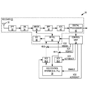
Figure 3 illustrates one example of the wireless device 18 according to
some embodiments of the present disclosure. Note that in this example, the
wireless device 18 is illustrated as including a receiver 22. Note, however,
that
the concepts disclosed herein are equally applicable to the use of X0s to
generate Local Oscillator (LO) signals for a transmitter(s) and/or receiver(s)
of
the wireless device 18. As illustrated, the wireless device 18 includes the
receiver 22, a control unit 24, a first XO (X01) 26-1 that outputs a reference
.. signal having a first reference frequency, a second XO (X02) 26-2 that
outputs a
reference signal having a second reference frequency that is greater than the
CA 03047613 2019-06-19
WO 2018/113903
PCT/EP2016/081750
12
first reference frequency, and a X02 control system 28. As an example, the
first
reference frequency is less than 52 MHz (e.g., in the range of and including
20 to
40 MHz), and the second reference frequency is greater than or equal to 100
MHz. The control unit 24 is implemented in hardware or a combination of
hardware and software. For example, the control unit 24 may be implemented as
a processing circuit that includes one or more processors (e.g., Central
Processing Units (CPUs), Application Specific Integrated Circuits (ASICs),
Field
Programmable Gate Arrays (FPGAs), or the like), where the processing circuit
executes software that causes the control unit 24 to thereby provide the
functionality of the control unit 24 described herein.
While the receiver 22 may include various analog and digital circuits, in
the illustrated example, the receiver 22 includes an antenna(s) 30, a Band-
Pass
Filter (BPF) 32, a Low-Noise Amplifier (LNA) 34, a mixer 36, a BPF 38, an
Analog-to-Digital Converter (ADC) 40, and a digital processor 42. In addition,
the
receiver 22 includes a Radio Frequency (RF) PLL 44 that controls a Controlled
Oscillator (CO) 46 to provide a LO signal to the mixer 36. In operation, a RF
receive signal is received via the antenna 30 and filtered by the BPF 32 to
thereby provide a filtered, RF receive signal. The filtered, RF receive signal
is
amplified by the LNA 34 to provide an amplified and filtered RF receive
signal,
which is then downconverted from RF to, in this example, baseband at the mixer
36. In order to provide this downconversion from RF to baseband, the RF PLL
44 is configured by the control unit 24 such that, based on a reference
frequency
provided by either the X01 26-1 or the X02 26-2 depending on the
configuration,
the LO signal output by the CO 46 is equal to the carrier frequency fc of a
desired
receive signal. Note, however, that downconversion may alternatively be to a
desired Intermediate Frequency (IF), in which case the frequency of the LO
signal generated by the CO 46 is controlled to be the appropriate frequency
needed for downconversion from fc to the desired IF.
As discussed below, the control unit 24 configures the receiver 22 to use
either the X01 26-1 or the X02 26-2 based on one or more criteria. The one or
more criteria may include, for example, a synchronization state of the
wireless
CA 03047613 2019-06-19
WO 2018/113903
PCT/EP2016/081750
13
device 18, a connection state of the wireless device 18 (e.g., Radio Resource
Control (RRC) IDLE or RRC CONNECTED), and/or the carrier frequency fc of
the desired receive signal (i.e., the carrier frequency of the radio access
node
14). Thus, in one configuration, the control unit 24 configures the RF PLL 44
to
use the X01 26-1. In the illustrated example, this configuration of the RF PLL
44
to use the X01 26-1 includes closing a switch 48-1 and configuring settings
(e.g.,
divider value(s)) of the RF PLL 44 such that the RF PLL 44 will control the CO
46
to provide the desired LO frequency based on the reference frequency of the
X01 26-1. In another configuration, the control unit 24 configures the RF PLL
44
to use the X02 26-2. In the illustrated example, this configuration of the RF
PLL
44 to use the X02 26-2 includes closing a switch 48-2 and configuring settings
(e.g., divider value(s)) of the RF PLL 44 such that the RF PLL 44 will control
the
CO 46 to provide the desired LO frequency based on the reference frequency of
the X02 26-2. In some embodiments, prior to configuring the receiver 22 to use
the X02 26-2, the X02 control system 28, which may be implemented as a PLL,
is enabled and operates to adapt the X02 26-2 based on the signal output by
the
X01 26-1. In this case, the X01 26-1 has previously be adapted, or tuned,
according to the carrier frequency of the radio access node 14 and, as such,
can
be used to provide initial adaptation, or tuning, of the X02 26-2 prior to the
X02
26-2 being connected to the RF PLL 44.
Thus, the control unit 24 can intelligently control which of the X0s 26-1
and 26-2 is used by the receiver 22 based on the one or more criteria. In
doing
so, various advantages can be realized. For example, the control unit 24 can
configure the receiver 22 to use the X01 26-1 and deactivate the X02 26-2 when
in an 00S (out-of-sync) state, when in IDLE mode, and/or when operating at a
low carrier frequency (e.g., fc < 4 GHz or, as another example, fc < 10 GHz)
and
configure the receiver 22 to use the X02 26-2 and optionally deactivate the
X01
26-1 when in an in-sync state, when in a connected mode, and/or when
operating at a high carrier frequency (e.g., fc 4 GHz or, as another example,
fc
10 GHz). In this manner, power consumption can be reduced and, in some
embodiments, the amount of time needed to synchronize to the network can be
CA 03047613 2019-06-19
WO 2018/113903
PCT/EP2016/081750
14
reduced by using the X01 26-1, which has a smaller tolerance than the X02 26-
2, during synchronization. Note that these advantages are only examples.
Note that while the use of the X0s 26-1 and 26-2 is illustrated in the
example of Figure 3 as being used by the RF PLL 44 for controlling the LO
signal
for the receiver 22, the X0s 26-1 and 26-2 may additionally or alternatively
be
used by an RF PLL to provide a LO signal used for upconversion in a
transmitter
(not shown) of the wireless device 18.
Figure 4 is a flow chart that illustrates the operation of the wireless device
18 and, in particular, the control unit 24 to control the receiver 22 to use
either
the X01 26-1 or the X02 26-2 according to some embodiments of the present
disclosure. Optional steps are illustrated in dashed boxes. As illustrated,
the
control unit 24 decides whether the receiver 22 should be configured to use
the
X01 26-1 or the X02 26-2 (step 100). As discussed below, in some
embodiments, this decision is based on a synchronization state of the wireless
device 18 towards a radio access node 14, a connection state of the wireless
device 18 (e.g., RRC IDLE (Dormant State) or RRC CONNECTED or similar
states), and/or the carrier frequency fc of the desired receive signal (i.e.,
the
carrier frequency of the radio access node 14). More specifically, in some
embodiments, the control unit 24 decides that the receiver 22 is to use the
X01
26-1 if the wireless device 18 is in an 00S state and use the X02 26-2 if the
wireless device 18 is in an in-sync state. In some other embodiments, the
control
unit 24 decides that the receiver 22 is to use the X01 26-1 if the wireless
device
18 is in one connection state (e.g., an idle or dormant state) and use the X02
26-
2 if the wireless device 18 is in another state (e.g., a connected or active
state).
In some other embodiments, the control unit 24 decides that the receiver 22 is
to
use the X01 26-1 if the carrier frequency fc used by the radio access node 14
is
less than a predefined or preconfigured threshold (e.g., 4 GHz or 10 GHz) and
use the X02 26-2 if the carrier frequency fc is greater than or equal to the
predefined or preconfigured threshold.
The control unit 24 then configures the receiver 22 in accordance with the
decision made in step 100. More specifically, upon deciding that the receiver
22
CA 03047613 2019-06-19
WO 2018/113903
PCT/EP2016/081750
is to use the X01 26-1, the control unit 24 activates the X01 26-1 by, e.g.,
asserting the XO activation signal (see X01 ACT/DEACT in Figure 3) if the X01
26-1 is not already activated (step 102). Note that, in some embodiments, the
X01 26-1 is always activated, in which case step 102 does not need to be
5 performed. In some other embodiments, the X01 26-1 may at times be
deactivated, in which case the control unit 24 activates the X01 26-1 if the
X01
26-1 is not already activated.
Once the X01 26-1 is activated, the control unit 24 configures the receiver
22 to use the X01 26-1 (step 104). The exact manner in which the receiver 22
is
10 configured to use the X01 26-1 will vary depending on the particular
implementation of the receiver 22, as will be appreciated by one of ordinary
skill
in the art. However, in the example of Figure 3, the control unit 24
configures the
receiver 22 to use the X01 26-1 by connecting the X01 26-1 to the RF PLL 44
by, in this example, closing the switch 48-1 and configuring the RF PLL 44
(e.g.,
15 configuring one or more settings of the RF PLL 44 such as, for example,
one or
more divider values) based on the frequency of the X01 26-1 such that the CO
46 is controlled to provide the desired LO frequency. As a simple, non-
limiting
example, the output frequency of the CO 46 is controlled by the RF PLL 44 to
be
N times the reference frequency. So, if the X01 26-1 is connected to the RF
PLL
44, the RF PLL 44 controls the CO 46 such that the output frequency of the CO
46 is N times the frequency of the X01 26-1. Therefore, in this example, the
control unit 24 configures the parameter N of the RF PLL 44 such that N times
the frequency of the X01 26-1 is equal to the desired LO frequency, which for
direct downconversion to baseband is equal to the carrier frequency fc. After
configuring the receiver 22 to use the X01 26-1, the control unit 24
optionally
deactivates the X02 26-2 if the X02 26-2 was active by, e.g., de-asserting the
X02 ACT/DEACT signal (see Figure 3) (step 106). By deactivating the X02 26-
2, power consumption is reduced.
Returning to step 100, upon deciding that the receiver 22 is to use the
X02 26-2, the control unit 24 activates the X01 26-1 by, e.g., asserting the
XO
activation signal (see X01 ACT/DEACT in Figure 3) if the X01 26-1 is not
CA 03047613 2019-06-19
WO 2018/113903
PCT/EP2016/081750
16
already activated (step 108). Note that, in some embodiments, the X01 26-1 is
always activated, in which case step 108 does not need to be performed. In
some other embodiments, the X01 26-1 may at times be deactivated, in which
case the control unit 24 activates the X01 26-1 if the X01 26-1 is not already
activated. Also, in this example, the X01 26-1 is first tuned and then used to
tune the X02 26-2. As such, the X01 26-1 is activated in step 108. However, in
other embodiments, the X02 26-2 is not tuned based on the X01 26-1 and, as
such, step 108 is not needed.
The control unit 24 activates the X02 26-2 by, e.g., asserting the XO
activation signal (see X02 ACT/DEACT in Figure 3) if the X02 26-2 is not
already activated (step 110). Note that, in some embodiments, the X02 26-2 is
always activated, in which case step 110 does not need to be performed. In
some other embodiments, the X02 26-2 may at times be deactivated, in which
case the control unit 24 activates the X02 26-2 if the X02 26-2 is not already
.. activated. In this example embodiment, the control unit 24 causes
adaptation of
the X02 26-2 using the X01 26-1 (step 112). For example, if the wireless
device
18 is not already synchronized to the carrier frequency fc of the radio access
node 14, the control unit 24 may first configure the receiver 22 to use the
X01
26-1 as described above and perform an initial synchronization process whereby
.. the X01 26-1 and the LO signal are tuned to the carrier frequency fc. Once
the
wireless device 18 is synchronized to the radio access node 14 either as part
of
step 112 or as part of a previously performed synchronization process and the
X02 26-2 is activated, the control unit 24 enables the X02 control system 28.
The X02 control system 28 may be, for example, a PLL or some other circuitry
that adapts, e.g., a voltage or digital setting of the X02 26-2 to track the
frequency of the X01 26-1. For example, if the X01 frequency is 26 MHz and
the X02 frequency is desired to be 104 MHz and if the X01 26-1 is fine-tuned
during synchronization to the carrier frequency fc, then this fine-tuning can
at
least initially be performed for the X02 26-2 by adapting the X02 26-2 such
that
its output frequency is exactly four times the X01 frequency, in this example.
CA 03047613 2019-06-19
WO 2018/113903
PCT/EP2016/081750
17
Once the X02 26-2 is activated and, optionally, adapted using the X01
26-1, the control unit 24 configures the receiver 22 to use the X02 26-2 (step
114). The exact manner in which the receiver 22 is configured to use the X02
26-2 will vary depending on the particular implementation of the receiver 22,
as
will be appreciated by one of ordinary skill in the art. However, in the
example of
Figure 3, the control unit 24 configures the receiver 22 to use the X02 26-2
by
connecting the X02 26-2 to the RF PLL 44 by, in this example, closing the
switch
48-2 and configuring the RF PLL 44 (e.g., configuring one or more settings of
the
RF PLL 44 such as, for example, one or more divider values) based on the
frequency of the X02 26-2 such that the CO 46 is controlled to provide the
desired LO frequency. As a simple, non-limiting example, the output frequency
of the CO 46 is controlled by the RF PLL 44 to be N times the reference
frequency. So, if the X02 26-2 is connected to the RF PLL 44, the RF PLL 44
controls the CO 46 such that the output frequency of the CO 46 is N times the
frequency of the X02 26-2. Therefore, in this example, the control unit 24
configures the parameter N of the RF PLL 44 such that N times the frequency of
the X02 26-2 is equal to the desired LO frequency, which for direct
downconversion to baseband is equal to the carrier frequency fc. After
configuring the receiver 22 to use the X02 26-2, the control unit 24
optionally
deactivates the X01 26-1 if the X01 26-1 was active by, e.g., de-asserting the
X01 ACT/DEACT signal (see Figure 3) (step 116). By deactivating the X01 26-
1, power consumption is reduced.
Whether using the X01 26-1 or the X02 26-2, the control unit 24
determines whether an XO change event has occurred (step 118). In other
words, the control unit 24 determines whether an event that may result in a
change in which of the X0s 26-1 and 26-2 is to be used has occurred. For
example, in some embodiments, the control unit 24 decides which XO to use
based on the sync state of the wireless device 18 and, as such, the control
unit
24 detects an XO change event when the sync state of the wireless device 18
changes. In some other embodiments, the control unit 24 decides which XO to
use based on a connection state of the wireless device 18 and, as such, the
CA 03047613 2019-06-19
WO 2018/113903
PCT/EP2016/081750
18
control unit 24 detects an XO change event when the connection state of the
wireless device 18 changes. In yet another example, in some embodiments, the
control unit 24 decides which XO to use based on the carrier frequency fc and,
as such, the control unit 24 detects an XO change event when the carrier
frequency fc changes or when an event (e.g., a handover) that may result in a
change in the carrier frequency fc has occurred. If no XO change event is
detected, the control unit 24 continues to monitor for an XO change event. If
an
XO change event is detected, the process returns to step 100 where the control
unit 24 decides whether to use the X01 26-1 or the X02 26-2. The process then
continues as described above.
Figure 5 is a flow chart that illustrates the operation of the wireless device
18 and in particular the control unit 24 according to some embodiments of the
present disclosure. This process is one particular implementation of the
process
of Figure 4. In general, using the process of Figure 5, the control unit 24
configures the receiver 22 to use the X01 26-1 during initial synchronization
to
the carrier frequency fc of the radio access node 14. Once synchronization is
complete, the control unit 24 configures the receiver 22 to use the X02 26-2.
Before discussing the process of Figure 5 in detail, a brief discussion of
some problems associated with using a high frequency XO during initial
synchronization is presented. The larger uncertainty in frequency (i.e., the
larger
tolerance) for high frequency X0s (i.e., >100 MHz X0s) substantially impacts
the
time it takes to reach initial synchronization with the network and may also
pose
a problem in handover events. For instance, assuming a carrier frequency of 2
GHz, a 26 MHz XO has an initial uncertainty of 10 parts-per-million (ppm). To
do
initial cell search in LTE/ Wideband Code Division Multiple Access (WCDMA)
High Speed Packet Access (HSPA), a frequency gridding around a hypothesized
carrier frequency is needed, with a frequency grid of around 10 kilohertz
(kHz).
Hence, up to five to six searches are needed for each possible carrier
frequency.
Once the synchronization signal (e.g., Primary Synchronization Signal /
Secondary Synchronization Signal (PSS/SSS), Primary Synchronization Channel
/ Secondary Synchronization Channel (P-SCH/S-SCH)) is detected for a certain
CA 03047613 2019-06-19
WO 2018/113903
PCT/EP2016/081750
19
frequency hypothesis, the XO can be adjusted and the correct carrier frequency
(e.g., below 100 Hertz (Hz) error) can be achieved. For a 200 MHz XO, the
corresponding search grid should be four to five times larger (i.e., 20 to 30
frequency hypothesis for each carrier assuming 2 GHz, for higher carrier
.. frequency even more frequency hypothesis). Hence, the initial
synchronization
time might be much longer using >100 MHz X0s. Conversely, using 26 MHz
X0s for initial synchronization will reduce initial synchronization time, but
could
not manage the stringent phase noise requirements needed for 1+ gigabits per
second (Gb/s) data rates above 10 GHz carrier frequency. Using the process of
Figure 5, the wireless device 18 addresses these problems.
As illustrated in Figure 5, prior to synchronization, the control unit 24
activates the X01 26-1 if not already activated and configures the receiver 22
to
use the X01 26-1 (step 200). More specifically, the control unit 24 activates
the
X01 26-1 by, e.g., asserting the XO activation signal (see X01 ACT/DEACT in
Figure 3) if the X01 26-1 is not already activated. Note that, in some
embodiments, the X01 26-1 is always activated, in which case the X01 26-1
does not need to be activated in step 200. In some other embodiments, the X01
26-1 may at times be deactivated, in which case the control unit 24 activates
the
X01 26-1 if the X01 26-1 is not already activated. Once the X01 26-1 is
activated, the control unit 24 configures the receiver 22 to use the X01 26-1.
The exact manner in which the receiver 22 is configured to use the X01 26-1
will
vary depending on the particular implementation of the receiver 22, as will be
appreciated by one of ordinary skill in the art. However, in the example of
Figure
3, the control unit 24 configures the receiver 22 to use the X01 26-1 by
connecting the X01 26-1 to the RF PLL 44 by, in this example, closing the
switch
48-1 and configuring the RF PLL 44 (e.g., configuring one or more settings of
the
RF PLL 44 such as, for example, one or more divider values) based on the
frequency of the X01 26-1 such that the CO 46 is controlled to provide the
desired LO frequency. While not illustrated, after configuring the receiver 22
to
use the X01 26-1, the control unit 24 optionally deactivates the X02 26-2 if
the
CA 03047613 2019-06-19
WO 2018/113903
PCT/EP2016/081750
X02 26-2 was active by, e.g., de-asserting the X02 ACT/DEACT signal (see
Figure 3). By deactivating the X02 26-2, power consumption is reduced.
The receiver 22 is enabled (if needed), and the control unit 24 configures
the receiver 22 to receive at a (hypothesized) carrier frequency fc (step
202).
5 The carrier frequency fc may be determined by, e.g., the control unit 24
having
historical information on possible carrier frequencies for the radio access
nodes
14. This configuration of the receiver 22 includes connecting the X01 26-1 to
the
RF PLL 44 and configuring the RF PLL 24 (e.g., configuring a divider value(s)
for
the RF PLL 24) such that, based on the frequency of the X01 26-1, the RF PLL
10 44 controls the CO 46 to output the desired LO frequency.
Next, an initial cell search/scan is performed, where the wireless device 18
searches for synchronization signals (e.g., PSS/SSS in LTE for instance)
transmitted by a radio access node 14 (step 204). Cell search procedures are
well known in the art and, as such, the cell search procedure is not described
15 here. The control unit 24 determines whether a synchronization signal
has been
detected (step 206). In this manner, the control unit 24 is deciding whether
to
configure the wireless device 18 to use the X02 26-2 or to continue to use the
X01 26-1. This step is therefore one example implementation of step 100 of
Figure 4. If a synchronization signal has not been detected, the control unit
24
20 updates the (hypothesized) carrier frequency fc (step 208) and the
process
returns to step 202. Once a synchronization signal is detected, the control
unit
24 may adapt or fine tune the X01 26-1 and, in particular, the LO frequency to
the carrier frequency fc of the received signal (step 210). Again, this
adaption
process is well known in the art and, as such, the details are not repeated
herein.
However, in general, this adaptation may be performed by adapting the RF PLL
44 (e.g., adapting the divider value(s) of the RF PLL 44) and/or by adapting
the
X01 26-1 via, e.g., a voltage or digital setting of the X01 26-1. For direct
downconversion of the received signal from the carrier frequency fc to
baseband,
this adaptation results in the LO frequency being substantially matched to the
actual carrier frequency fc of the receive signal to within some predefined
tolerance (e.g., 100 Hz). In addition or alternatively, the adaptation may be
CA 03047613 2019-06-19
WO 2018/113903
PCT/EP2016/081750
21
performed by configuring a de-rotator in the digital processor 42 to
compensate
for the frequency error in the digital domain.
Once synchronization is complete, the X02 26-2 is activated (step 212)
and adapted based on the X01 26-1 (e.g., the output of the X01 26-1) (step
214). More specifically, in the example of Figure 3, the X02 control system 28
is
activated (if not already active). The X02 control system 28 then adapts the
X02
26-2 based on, in this example, the output of X01 26-1 to thereby fine tune
the
frequency of the X02 26-2. The X02 control system 28 may be, for example, a
PLL and the X01 26-1 serves as a reference for this PLL and this PLL in turn
controls, e.g., a voltage or digital setting of the X02 26-2 to track the
frequency of
the X01 26-1.
Once the X02 26-2 is active and tuned, the control unit 24 configures the
receiver 22 to perform further signal reception using the X02 26-2 (step 216).
In
other words, the control unit 24 configures the receiver 22 to use the X02 26-
2.
Again, as discussed above, the exact manner in which the receiver 22 is
configured to use the X02 26-2 will vary depending on the particular
implementation of the receiver 22, as will be appreciated by one of ordinary
skill
in the art. However, in the example of Figure 3, the control unit 24
configures the
receiver 22 to use the X02 26-2 by connecting the X02 26-2 to the RF PLL 44
by, in this example, closing the switch 48-2 and configuring the RF PLL 44
(e.g.,
configuring one or more settings of the RF PLL 44 such as, for example, one or
more divider values) based on the frequency of the X02 26-2 such that the CO
46 is controlled to provide the desired LO frequency.
After configuring the receiver 22 to use the X02 26-2, the control unit 24
optionally deactivates the X01 26-1 by, e.g., de-asserting the X01 ACT/DEACT
signal (see Figure 3) (step 218). Notably, step 218 may be performed if the
control input to the X02 26-2 can be held constant while disabling the X02
control system 28. Alternatively, the X01 26-1 is kept active as an input to
the
X02 control system 28 that in turn continuously maintains lock between the X02
26-2 and the X01 26-1.
CA 03047613 2019-06-19
WO 2018/113903
PCT/EP2016/081750
22
Optionally, in some embodiments, the control unit 24 monitors the
synchronization state of the wireless device 18 (step 220). Once the wireless
device 18 is determined to be 00S, the process returns to step 200 and is
repeated. The wireless device 18 may be determined to be 00S based on any
suitable criteria such as, e.g.,
= Long DRX cycles where the X02 26-2 has been disabled for power
saving purposes,
= Large temperature variations (e.g., due to turning a power amplifier
of the wireless device 18 on or off), and/or
= Being 00S in terms of no reliable reception of data from the radio
access node 14 (i.e., a Radio Link Failure (RLF) or a radio link
problem).
Figure 6 is a flow chart that illustrates the operation of the wireless device
18 and, in particular, the control unit 24 according to some embodiments of
the
present disclosure. This embodiment is similar to that of Figure 4 but where
the
decision as to which of the X0s 26-1 and 26-2 to be used is based on a
connection state of a connection of the wireless device 18 to a radio access
node
14. As illustrated, the control unit 24 determines a connection state of the
wireless device 18 with respect to a serving or camping cell or beam (step
300).
In some embodiments, the connection state is either idle state or connected
state. For example, for LTE, the connection state is the RRC state, which can
be
either IDLE (or Dormant in 5G NR) or CONNECTED (or active). However, other
wireless systems may have different connection states. For example, in 5G,
there may be more than two connection states.
The control unit 24 then decides which XO to use based on the connection
state of the wireless device 18 (step 302). For example, in some embodiments,
the control unit 24 decides to use the X01 26-1 if the wireless device 18 is
in one
connection state (e.g., idle state such as, for example, RRC IDLE in LTE) and
decides to use the X02 26-2 if the wireless device 18 is in another connection
state (e.g., connected state such as, for example, RRC CONNECTED in LTE).
Note that the terms "idle" and "connected" state as used herein are only
CA 03047613 2019-06-19
WO 2018/113903
PCT/EP2016/081750
23
examples. Other names for different connection states may be used, such as
dormant and active, particularly in future cellular communications networks
(e.g.,
5G networks). The key is that the receiver 22 is configured to use different
X0s
26-1, 26-2 in different connection states, which enables the lower-frequency
X01
26-1 to be used when desirable or beneficial to do so (e.g., when using low
data
rates, paging, long DRX (power saving reason and short resync time needed))
and enables the higher-frequency X02 26-2 to be used when desirable or
beneficial to do so (e.g., when high performance reception is desired such as,
e.g., reception using MIMO, higher order modulation, etc.). The process then
proceeds as described above with respect to Figure 4 to either use the X01 26-
1
(steps 304-308, which correspond to steps 202-206 of Figure 4) or use the X02
26-2 (steps 310-318, which correspond to steps 108-116 of Figure 4) in
accordance with the decision made in step 302. The control unit 24 then
decides
whether the connection state of the wireless device 18 has changed (step 320).
If not, the control unit 24 continues to monitor for a change in the
connection
state. Upon detecting a change in the connection state, the process then
proceeds to step 302 and is repeated taking into consideration the new
connection state of the wireless device 18.
With respect to the process of Figure 6, the idea is that in idle mode,
.. where only paging and mobility measurement are needed, the lower frequency
X01 26-1 can be used since such transmissions are typically single layer and
low order Modulation and Coding Scheme (MCS), and since sync is shorter (less
drift between DRX cycles). Thus, by using the process of Figure 6, the low-
frequency X01 26-1 is used if the wireless device 18 is in idle mode, and the
high-frequency X02 26-2 is used if the wireless device 18 is in connected
mode.
Figure 7 is a flow chart that illustrates the operation of the wireless device
18 and, in particular, the control unit 24 according to some embodiments of
the
present disclosure. This embodiment is similar to that of Figure 4 but where
the
decision as to which of the X0s 26-1 and 26-2 to be used is based on the
carrier
frequency fc of the received signal. As illustrated, the control unit 24
determines
the carrier frequency fc of the received signal or the signal to be received
(step
CA 03047613 2019-06-19
WO 2018/113903
PCT/EP2016/081750
24
400). The control unit 24 then decides which XO to use based on the carrier
frequency fc (step 402). For example, in some embodiments, the control unit 24
decides to use the X01 26-1 if the carrier frequency fc is less than a
predefined
or preconfigured threshold and decides to use the X02 26-2 if the carrier
frequency fc is greater than the predefined or preconfigured threshold. The
predefined or preconfigured threshold may vary but, as one example, this
threshold may be 4 GHz or 10 GHz.
It should be noted that, in some embodiments, the wireless device 18 may
include separate receivers (i.e., as part of separate transceivers) for
different
carrier frequencies. For example, the wireless device 18 may include a first
transceiver for carrier frequencies that are less than, e.g., 6 GHz and a
second
transceiver for carrier frequencies that are greater than or equal to, e.g., 6
GHz.
In this example, the X01 26-1 could be used for either transceiver, whereas
the
X02 26-2 may only be used for the higher frequency transceiver (e.g., the > 6
GHz transceiver or millimeter wave (mmW) transceiver). Thus, in this example,
if
the desired carrier frequency fc is less than, e.g., 6 GHz, then the first,
lower
frequency transceiver is used and, as such, the control unit 24 configures the
receiver of the first, lower-frequency transceiver to use the X01 26-1.
Conversely, if the desired carrier frequency fc is greater than, e.g., 6 GHz,
then
the second, higher-frequency transceiver is used and, as such, the control
unit
24 configures the receiver of the second, higher-frequency transceiver to use
the
X02 26-2 or, in some embodiments, either the X01 26-1 or the X02 26-2 based
on, e.g., synchronization state and/or connection state, as described above.
Thus, in this example, the control unit 24 decides which receiver to use and
which XO to use based on the desired carrier frequency fc.
The process then proceeds as described above with respect to Figure 4 to
either use the X01 26-1 (steps 404-408, which correspond to steps 202-206 of
Figure 4) or use the X02 26-2 (steps 410-418, which correspond to steps 108-
116 of Figure 4) in accordance with the decision made in step 402. The control
unit 24 then decides whether a handover (HO) over is to be performed (e.g.,
whether a handover command has been received) (step 420). The handover can
CA 03047613 2019-06-19
WO 2018/113903
PCT/EP2016/081750
be an inter-frequency handover or an inter-Radio Access Technology (RAT)
handover, for example. The handover is from one cell or beam (source) to
another cell or beam (target). The target may operate on a different carrier
frequency than the source and, as such, the control unit 24 re-evaluates which
5 XO to use. In other words, a handover indicates that there may be a new
carrier
frequency fc. Thus, if a handover is to be performed, the process returns to
step
400 to determine the new carrier frequency fc for the target cell or beam and
then
repeated taking into consideration the new carrier frequency fc.
The following acronyms are used throughout this disclosure.
10 = 2G Second Generation
= 3G Third Generation
= 3GPP Third Generation Partnership Project
= 4G Fourth Generation
= 5G Fifth Generation
15 = ADC Analog-to-Digital Converter
= ASIC Application Specific Integrated Circuit
= BPF Band-Pass Filter
= BPSK Binary Phase Shift Keying
= CMOS Complementary Metal-Oxide-Semiconductor
20 = CN Core Network
= CO Controlled Oscillator
= CPU Central Processing Unit
= dB Decibel
= dBc/Hz Decibels Relative to the Carrier per
Hertz
25 = DRX Discontinuous Reception
= eNB Enhanced or Evolved Node B
= FoM Figure of Merit
= FPGA Field Programmable Gate Array
= Gb/s Gigabits per Second
= GHz Gigahertz
CA 03047613 2019-06-19
WO 2018/113903
PCT/EP2016/081750
26
= HO Handover
= HSPA High Speed Packet Access
= Hz Hertz
= IF Intermediate Frequency
= kHz Kilohertz
= LNA Low-Noise Amplifier
= LO Local Oscillator
= LIE Long Term Evolution
= MA-MIMO Multi-Antenna Multiple Input Multiple
Output
= MBB Mobile Broadband
= MCS Modulation and Coding Scheme
= MHz Megahertz
= MME Mobility Management Entity
= mmW Millimeter Wave
= MTC Machine Type Communication
= mW Milliwatt
= 00S Out-of-Sync
= PDN Packet Data Network
= P-GW Packet Data Network Gateway
= PLL Phase Locked Loop
= PPm Part-Per-Million
= P-SCH Primary Synchronization Channel
= PSS Primary Synchronization Signal
= QAM Quadrature Amplitude Modulation
= RAN Radio Access Network
= RAT Radio Access Technology
= RF Radio Frequency
= RLF Radio Link Failure
= RRC Radio Resource Control
= SCEF Service Capability Exposure Function
CA 03047613 2019-06-19
WO 2018/113903
PCT/EP2016/081750
27
= SNR Signal-to-Noise Ratio
= S-SCH Secondary Synchronization Channel
= SSS Secondary Synchronization Signal
= UE User Equipment
= VCO Voltage Controlled Oscillator
= WCDMA Wideband Code Division Multiple Access
= XO Reference Crystal Oscillator
Those skilled in the art will recognize improvements and modifications to
the embodiments of the present disclosure. All such improvements and
modifications are considered within the scope of the concepts disclosed herein
and the claims that follow.