Note: Descriptions are shown in the official language in which they were submitted.
CA 03047882 2019-06-20
- 1 -
Description
Title: OPTICAL TRANSMISSION CHARACTERISTIC ESTIMATION METHOD, OPTICAL
TRANSMISSION CHARACTERISTIC COMPENSATION METHOD, OPTICAL
TRANSMISSION CHARACTERISTIC ESTIMATION SYSTEM AND OPTICAL
TRANSMISSION CHARACTERISTIC COMPENSATION SYSTEM
Field
[0001]
The present invention relates to an optical transmission characteristic
estimation method,
an optical transmission characteristic compensation method, an optical
transmission characteristic
estimation system, and an optical transmission characteristic compensation
system estimating or
compensating the transmission characteristics of an optical transceiver in
optical communication.
Background
[0002]
To cope with increase of communication traffic, increase of speed and capacity
of an
optical transceiver is demanded. In recent years, the optical transceiver
increasingly introduced
uses a digital coherent technology that is combination of digital signal
processing (DSP) and
coherent detection.
[0003]
The optical transceiver of a transmission rate of 100 Gb/s per one channel
uses, for
example, a modulation system of PDM-QPSK (polarization division multiplexing-
quadrature
phase shift keying) at Baud rate of 32 Gbaud. An optical transmitter modulates
each of linear
polarized light (X-polarized wave and Y-polarized wave) orthogonal to each
other by QPSK
baseband signals to generate PDM-QPSK optical signals. An optical receiver
converts the
received optical signals into baseband signals through the coherent detection
of the optical signals
and local oscillation light, and demodulates the QPSK by the digital signal
processing (DSP) to
reproduce transmission data.
CA 03047882 2019-06-20
- 2 -
[0004]
To increase the transmission capacity per one channel, the optical transceiver
of a
transmission rate of 400 Gb/s uses, for example, a modulation system of PDM-
16QAM
(polarization division multiplexing-16 quadrature amplitude modulation) at
Baud rate of 64
Gbaud, or a modulation system of PDM-64QAM at Baud rate of 43 Gbaud. As
described above,
in the future optical transceiver, increase of Baud rate and multi-valuing of
the modulation system
progress in order to increase the transmission capacity per one channel.
[0005]
The optical transceiver is required to have excellent transmission
characteristics in a wide
range along with increase of Baud rate and multi-valuing. The transmission
characteristics of a
transmission signal in the optical transceiver are represented by a transfer
function. The optical
transceiver generally includes a plurality of lanes (in-phase component XI of
X-polarized wave,
quadrature component XQ of X-polarized wave, in-phase component YI of Y-
polarized wave,
and quadrature component YQ of Y-polarized wave), and is required to
sufficiently suppress
difference of the transfer function among the lanes because the difference of
the transfer function
among the lanes causes deterioration of total transmission characteristics of
the system. In a
case where frequency characteristics of the transfer function of the optical
transceiver are
insufficient or a case where the frequency characteristics are different among
the lanes, it is
necessary to compensate the transmission characteristics or the difference
among the lanes by, for
example, the DSP. On this issue, a method in which chromatic dispersion of an
optical
transmission line or the difference among the lanes on reception side is
compensated by the
reception side (for example, see NPLs 1 and 2), and a method in which the
difference among the
lanes on transmission side is compensated by the transmission side (for
example, see PTL 1 and
NPL 3) have been proposed.
Citation List
Patent Literature
[0006]
[PTL 1] Japanese Patent No. 6077696
Non Patent Literature
[0007]
CA 03047882 2019-06-20
- 3 -
[NPL 1] R. R. Muller, J. Renaudier, "Blind Receiver Skew Compensation and
Estimation for
Long-Haul Non-Dispersion Managed Systems Using Adaptive Equalizer", JOURNAL OF
L1GHTWAVE TECHNOLOGY, VOL. 33, NO. 7, pp.1315-1318, APRIL 1,2015.
[NPL 2] J. C. M. Diniz, E. P da Silva, M. PieIs, and D. Zibar, "Joint IQ Skew
and Chromatic
Dispersion Estimation for Coherent Optical Communication Receivers", Advanced
Photonics
Congress 2016.
[NPL 3] Ginni Khanna, Bernhard Spinnler, Stefano Calabro, Erik De Man, and
Norbert Hanik,
"A Robust Adaptive Pre-Distortion Method for Optical Communication
Transmitters", IEEE
PHOTONICS TECHNOLOGY LETTERS, VOL. 28, NO. 7, pp.752-755, APRIL 1, 2016.
Technical Problem
[0008]
To compensate the transfer function of the optical transceiver by the DSP, it
is necessary
to previously grasp transfer functions of an optical circuit, an analog
electric circuit, and the like
of the optical transceiver, and to set a compensation value based on the
transfer functions as
necessary. The optical transmitter and the optical receiver each have
frequency characteristics
of the transfer function requiring compensation based on Baud Rate. In a case
where the
compensation value for compensation of the above-described transfer function
is set in an
existing optical transceiver, the compensation value is set to an optical
transmitter compensation
unit and a receiver compensation unit based on, for example, a specification
value of the transfer
function provided from an optical circuit vender or an analog electric circuit
vender or an
evaluation result of the previously-measured transfer function of a
representative individual,
which makes it possible to achieve sufficient total transmission
characteristics.
[0009]
In the high-speed transmission system of a transmission rate of 400 Gb/s or
the like, along
with the increase of Baud rate and the multi-valuing, the sufficient total
transmission
characteristics cannot be achieved by setting of the compensation value based
on the specification
value provided from the vender or the evaluation result of the representative
individual, due to
individual variation of the transfer function of the optical circuit or the
analog electric circuit.
CA 03047882 2019-06-20
-4 -
[0010]
The present invention is made to solve the above-described issues, and an
object of the
present invention is to provide an optical transmission characteristic
estimation method, an
optical transmission characteristic compensation method, an optical
transmission characteristic
estimation system, and an optical transmission characteristic compensation
system that each can
estimate or compensate transmission characteristics of an optical transceiver.
Solution to Problem
[0011]
An optical transmission characteristic estimation method according to the
present
invention estimating optical transmission characteristics of an optical
transceiver by an optical
transmission characteristic estimation system, includes: a first step of
estimating a transfer
function or an inverse transfer function of an optical transmitter from first
data acquired by a
reception unit when a first known signal is transmitted from a transmission
unit to the reception
unit of the optical transceiver, and a temporary transfer function or a
temporary inverse transfer
function of an optical receiver of the reception unit; and a second step of
estimating a transfer
function or an inverse transfer function of the optical receiver from second
data acquired by the
reception unit when a second known signal is transmitted from the transmission
unit to the
reception unit, and the estimated transfer function or the estimated inverse
transfer function of the
optical transmitter.
Advantageous Effects of Invention
[0012]
The present invention makes it possible to estimate transmission
characteristics of an
optical transceiver.
Brief Description of the Drawings
[0013]
Fig. 1 is a diagram illustrating an optical transceiver including the optical
transmission
characteristic estimation system and the optical transmission characteristic
compensation system
according to the embodiment of the present invention.
CA 03047882 2019-06-20
- 5 -
Fig. 2 is a flowchart illustrating the optical transmission characteristic
estimation method
according to the embodiment of the present invention.
Fig. 3 is a flowchart to estimate the temporary transfer function of the
optical receiver
according to the embodiment of the present invention.
Fig. 4 is a diagram illustrating a first receiver transfer function estimation
unit according
to an embodiment 1 of the present invention.
Fig. 5 is a diagram illustrating a receiver compensation unit according to the
embodiment
1 of the present invention.
Fig. 6 is a diagram illustrating a receiver compensation unit according to an
embodiment
2 of the present invention.
Fig. 7 is a diagram illustrating a receiver compensation unit according to an
embodiment
3 of the present invention.
Fig. 8 is a diagram illustrating a receiver compensation unit according to an
embodiment
4 of the present invention.
Fig. 9 is a diagram illustrating a first receiver transfer function estimation
unit according
to the embodiment 2 of the present invention.
Fig. 10 is a diagram illustrating a first receiver transfer function
estimation unit according
to the embodiment 3 of the present invention.
Fig. 11 is a diagram illustrating frequency response (amplitude information)
of the
temporary transfer function of the optical receiver according to the
embodiment of the present
invention.
Fig. 12 is a diagram illustrating frequency response (amplitude information)
of the
temporary inverse transfer function of the optical receiver according to the
embodiment of the
present invention.
Fig. 13 is a diagram illustrating the transmitter transfer function estimation
unit according
to the embodiment of the present invention.
Fig. 14 is a flowchart to acquire the transfer function or the inverse
transfer function of
the optical transmitter according to the embodiment of the present invention.
Fig. 15 is a diagram illustrating the time response of the inverse transfer
function of the
optical transmitter determined by the transmitter transfer function estimation
unit.
CA 03047882 2019-06-20
- 6 -
Fig. 16 is a diagram illustrating the frequency response (amplitude
characteristics and
phase characteristics) of the inverse transfer function of the optical
transmitter determined by the
transmitter transfer function estimation unit.
Fig. 17 is a diagram illustrating a second receiver transfer function
estimation unit
according to the embodiment 1 of the present invention.
Fig. 18 is a flowchart to estimate the true transfer function or the true
inverse transfer
function of the optical receiver according to the embodiment of the present
invention.
Fig. 19 is a diagram illustrating the time response of the inverse transfer
function of the
optical receiver determined by the second receiver transfer function
estimation unit.
Fig. 20 is a diagram illustrating the frequency response (amplitude
characteristics and
phase characteristics) of the inverse transfer function of the optical
receiver determined by the
second receiver transfer function estimation unit.
Fig. 21 is a diagram illustrating a second receiver transfer function
estimation unit
according to the embodiment 2 of the present invention.
Fig. 22 is a frequency spectrum after the compensation by the optical
transmission
characteristic compensation method according to the embodiment of the present
invention.
Fig. 23 is a diagram illustrating Q-value improvement effect after the
compensation by
the optical transmission characteristic compensation method according to the
embodiment of the
present invention.
Description of Embodiments
[0014]
An optical transmission characteristic estimation method, an optical
transmission
characteristic compensation method, an optical transmission characteristic
estimation system, and
an optical transmission characteristic compensation system according to an
embodiment of the
present invention are described with reference to drawings. Identical or
corresponding
components are denoted by the same reference numerals, and overlapped
description may be
omitted in some cases. Note that a term "transfer function" used in the
following description is
not limited to a predetermined function representing transmission
characteristics of an apparatus,
a component, a propagation path, and the like, and may indicate any of a
function, an expression,
a circuit, a line, and the like representing transmission characteristics
between given two points.
CA 03047882 2019-06-20
- 7 -
Further, the transfer function is not limited to a linear function, and may be
a function
representing nonlinear characteristics, or the like. Moreover, terms
"transmission" and
"transfer" are handled as the same meaning within the scope of the present
invention.
[0015]
Fig. 1 is a diagram illustrating an optical transceiver including the optical
transmission
characteristic estimation system and the optical transmission characteristic
compensation system
according to the embodiment of the present invention. A transmission unit 1
transmits an
optical signal to a reception unit 3 through a transmission line 2. The
transmission line 2
includes, for example, an optical fiber and an optical amplifier.
[0016]
The transmission unit 1 includes a transmission signal processing unit 4, a
known signal
insertion unit 5, a transmitter compensation unit 6, and an optical
transmitter 7. A part or all of
the transmission signal processing unit 4, the known signal insertion unit 5,
and the transmitter
compensation unit 6 are configured of hardware such as an ASIC (Application
Specific Integrated
Circuit) and an FPGA (Field-Programmable Gate Array). Further, a part or all
of the units may
be configured of software that functions when a processor such as a CPU
(Central Processing
Unit) executes a program stored in a storage unit.
[0017]
The known signal insertion unit 5 inserts a sequence of a known signal to a
modulation
target signal sequence of each of an XI lane (first lane), an XQ lane (second
lane), a YI lane (third
lane), and a YQ lane (fourth lane) that are generated by the transmission
signal processing unit 4.
The sequence of the known signal is shared by the transmission unit 1 and the
reception unit 3.
The known signal has predetermined bits or symbols, and for example, is
configured of a signal
sequence having about 2000 symbols. A length of the sequence of the known
signal is desired
to be at least longer than a length of a FIR filter to be calculated.
[0018]
The transmission signal processing unit 4 generates frame data based on
transmission data
sequence. The frame data is a signal sequence (modulation target signal
sequence) subjected to
modulation processing in the optical transmitter 7. The transmission signal
processing unit 4
transmits the frame data into which the known signal sequence has been
inserted, to the
transmitter compensation unit 6.
CA 03047882 2019-06-20
- 8 -
[0019]
The transmitter compensation unit 6 acquires an estimation result of a
transfer function of
the optical transmitter 7 from a transmitter transfer function estimation unit
8 of the reception unit
3 described below. The transmitter compensation unit 6 compensates the
transfer function of
each of the XI lane, the XQ lane, the YI lane, and the YQ lane of the optical
transmitter 7 and
difference of the transfer function among the lanes, based on the estimation
result. The
transmitter compensation unit 6 can be configured of a digital filter such as
an FIR (Finite
Impulse Response) filter; however, may be configured of an analog filter or
the like. Further,
the transmitter compensation unit 6 may include a function unit that has a
function to individually
compensate a delay time difference among the four lanes.
[0020]
The optical transmitter 7 modulates linear-polarized light orthogonal to each
other by the
compensated frame data, to generate an optical signal of the modulation target
signal sequence.
The optical transmitter 7 includes a driver amplifier 7a, a laser module 7b
(signal LD), a 90-
degree synthesizer 7c, and a polarization synthesizer 7d. The driver amplifier
7a amplifies an
electric signal of the compensated frame data so as to have an appropriate
amplitude, and
transmits the amplified electric signal to the 90-degree synthesizer 7c. The
90-degree
synthesizer 7c is a Mach-Zehnder vector modulator that separates linear-
polarized CW
(Continuous Wave) light transmitted from the laser module 7b into linear
polarized light
orthogonal to each other, and modulates the linear polarized light with the
frame data, thereby
generating the optical signals of the modulation target signal sequence. The
optical signal by the
horizontally polarized wave and the optical signal by the vertically polarized
wave are
synthesized by the polarization synthesizer 7d, and the synthesized signal is
supplied to the
reception unit 3 through the transmission line 2.
[0021]
The reception unit 3 includes an optical receiver 9, a data buffer 10, a
receiver
compensation unit 11, a reception signal processing unit 12, first and second
receiver transfer
function estimation units 13 and 14, and the transmitter transfer function
estimation unit 8. The
first and second receiver transfer function estimation units 13 and 14 and the
transmitter transfer
function estimation unit 8 configure the optical transmission characteristic
estimation system that
estimates optical transmission characteristics of the optical transceiver. The
optical transmission
CA 03047882 2019-06-20
- 9 -
characteristic estimation system, the transmitter compensation unit 6, and the
receiver
compensation unit II configure the optical transmission characteristic
compensation system that
compensates the optical transmission characteristics of the optical
transceiver. Note that, in Fig.
1, the transmitter compensation unit 6 and the receiver compensation unit 11
are each illustrated
as an individual block; however, the transmitter compensation unit 6 may be a
part of the
transmission signal processing unit 4, and the receiver compensation unit 11
may be a part of the
reception signal processing unit 12.
[0022]
The optical receiver 9 includes a polarization separator 9a, a laser module 9b
(local
oscillation LD), a polarization diversity 90-degree hybrid 9c, a photo diode
(PD, not illustrated), a
TIA (Transimpedance Amplifier) 9d, and an A/D converter 9e.
[0023]
The laser module 9b transmits the linear polarized CW light to the
polarization diversity
90-degree hybrid 9c. The polarization diversity 90-degree hybrid 9c causes
interference of the
received optical signal and the CW light. The photodiode photoelectrically
converts the
resultant optical signal. The TIA 9d converts a current signal to a voltage
signal. The A/D
converter 9e performs A/D conversion of the voltage signal. As a result, the
received optical
signal is converted into a baseband digital signal.
[0024]
A part or all of the A/D converter 9e of the optical receiver 9, the data
buffer 10, the
receiver compensation unit 11, the reception signal processing unit 12, the
first and second
receiver transfer function estimation units 13 and 14, and the transmitter
transfer function
estimation unit 8 are configured of hardware such as an ASIC and an FPGA.
Further, a part or
all of the units may be configured of software that functions when a processor
such as a CPU
executes a program stored in a storage unit. Further, the first and second
receiver transfer
function estimation units 13 and 14 and the transmitter transfer function
estimation unit 8 may be
configured of an external apparatus independent of the optical transceiver,
for example, a PC or
an apparatus equivalent thereto. Moreover, the reception signal processing
unit 12 may also
have a function similar to the function of each of the first and second
receiver transfer function
estimation units 13 and 14 and the transmitter transfer function estimation
unit 8, and may be
shared therebetween.
CA 03047882 2019-06-20
- 10 -
[0025]
The data buffer 10 is generally configured of a memory circuit (RAM), and
temporarily
stores the data as a result of the AID conversion of the received signal by
the optical receiver 9.
The data stored in the data buffer 10 is sequentially transmitted to the
receiver compensation unit
11 and the reception signal processing unit 12 on the post-stage. The first
and second receiver
transfer function estimation units 13 and 14 and the transmitter transfer
function estimation unit 8
may acquire the data. Note that the first and second receiver transfer
function estimation units
13 and 14 and the transmitter transfer function estimation unit 8 may directly
acquire the AID
converted data in real time without using the data buffer 10. In the
following, all of examples
described with use of the digital data of the data buffer 10 include the
method of directly
acquiring the reception data in real time.
[0026]
The receiver compensation unit 11 acquires the estimation result of the
transfer function
of the optical receiver 9 from the second receiver transfer function
estimation unit 14, and
compensates the transfer functions of the XI lane, the XQ lane, the YI lane,
and the YQ lane of
the optical receiver 9 and the difference of the transfer function among the
lanes, based on the
estimation result. The receiver compensation unit 11 is configured of a
digital filter such as an
FIR filter. Further, the receiver compensation unit 11 may include a function
unit that has a
function to individually compensate the delay time difference among the four
lanes.
[0027]
A digital signal is provided to the reception signal processing unit 12 from
the receiver
compensation unit 11. In the transmission line 2, waveform distortion occurs
on the optical
signal due to, for example, chromatic dispersion, polarization mode
dispersion, polarization
fluctuation, or nonlinear optical effect. The reception signal processing unit
12 compensates the
waveform distortion occurred in the transmission line 2. The reception signal
processing unit 12
also compensates difference between a frequency of the light from the laser
module 7b of the
optical transmitter 7 and a frequency of local oscillation light from the
laser module 9b of the
optical receiver 9. Further, the reception signal processing unit 12
compensates phase noise
based on a line width of the light from the laser module 7b of the optical
transmitter 7 and the line
width of the local oscillation light from the laser module 9b of the optical
receiver 9.
CA 03047882 2019-06-20
- 1 1 -
[0028]
The first receiver transfer function estimation unit 13 estimates a temporary
transfer
function or a temporary inverse transfer function of the optical receiver 9
from the digital data
that has been acquired by the reception unit 3 when an ASE (Amplified
Spontaneous Emission)
signal corresponding to white noise is input to an input end of the optical
receiver 9. The ASE
signal can be generated from an optical amplifier. In a case where only the
ASE signal is output,
the optical amplifier is used without any input. The optical amplifier may be
separately
prepared, or the optical amplifier of the transmission line 2 may be used. A
spectrum (frequency
characteristics) of the ASE signal is uniform. Therefore, the frequency
characteristics of the
optical receiver 9 are acquired through the input of the ASE signal.
Accordingly, the first
receiver transfer function estimation unit 13 acquires the data stored in the
data buffer 10 while
the ASE signal is input, which makes it possible to estimate the frequency
characteristics. The
frequency characteristics can be estimated for each lane. A configuration
example of the first
receiver transfer function estimation unit 13 is described below.
[0029]
The frequency characteristics are estimated as a transfer function by
performing Fourier
transform on the digital data. Examples of a method of determining the inverse
transfer function
include a method of determining a solution of an adaptive filter, in addition
to calculation of an
inverse. Examples of the method of determining the solution of the adaptive
filter generally
include a method of determining a Wiener solution and a method by LMS (least
mean square)
algorithm, RLS (recursive least square) algorithm, etc. In this case, the
transfer function is not
relatively changed with time. Therefore, "adaption" does not mean temporal
adaption. In the
following, "adaption" indicates adaption to a feedback circuit to determine a
convergent solution.
A detailed configuration example of the first receiver transfer function
estimation unit 13 is
described below. Although the ASE signal is used in the above description, the
signal is not
limited to the ASE signal, and any test signal can be used as long as the
spectrum of the signal is
known.
[0030]
The transmitter transfer function estimation unit 8 estimates the transfer
function or the
inverse transfer function of the optical transmitter 7 from first digital data
that has been acquired
by the reception unit 3 when a first known signal is transmitted from the
transmission unit 1 to
CA 03047882 2019-06-20
- 12 -
the reception unit 3, and the temporary transfer function or the temporary
inverse transfer
function of the optical receiver 9 of the reception unit 3. As the estimation
method, for example,
the transfer function of the optical transmitter 7 is estimated with use of an
adaptive filter. The
adaptive filter is, for example, a filter based on the LMS algorithm or a
filter based on the RMS
algorithm.
[0031]
The second receiver transfer function estimation unit 14 estimates a true
transfer function
or a true inverse transfer function of the optical receiver 9 from second
digital data that has been
acquired by the reception unit 3 when a second known signal is transmitted
from the transmission
unit 1 to the reception unit 3, and the estimated transfer function or the
estimated inverse transfer
function of the optical transmitter 7. As the estimation method, for example,
the inverse transfer
function of the optical receiver 9 is estimated with use of an adaptive
filter. The adaptive filter
is, for example, a filter based on the LMS algorithm or a filter based on the
RMS algorithm.
Also in this case, the estimation can be performed for each lane.
[0032]
Subsequently, a method of estimating the optical transmission characteristics
of the
optical transceiver by the optical transmission characteristic estimation
system according to the
present embodiment is described with reference to drawings. Fig. 2 is a
flowchart illustrating
the optical transmission characteristic estimation method according to the
embodiment of the
present invention. First, the first receiver transfer function estimation unit
13 estimates the
temporary transfer function or the temporary inverse transfer function of the
optical receiver 9
(step S1). Next, the transmitter transfer function estimation unit 8 estimates
the transfer function
or the inverse transfer function of the optical transmitter 7 (step S2). Next,
the second receiver
transfer function estimation unit 14 estimates the true transfer function or
the true inverse transfer
function of the optical receiver 9 (step S3).
[0033]
Next, detailed operation of each step is described. Fig. 3 is a flowchart to
estimate the
temporary transfer function of the optical receiver according to the
embodiment of the present
invention. First, the ASE signal is inserted into the input of the optical
receiver 9 (step S101).
Since the uniform spectrum of the ASE signal is known, the frequency
characteristics can be
acquired through insertion of the ASE signal. Next, the data buffer 10
acquires the reception
CA 03047882 2019-06-20
- 13 -
data while the ASE signal is input (step S102). Next, the first receiver
transfer function
estimation unit 13 acquires the digital data from the data buffer 10 and
performs the FFT
processing, thereby acquiring the temporary transfer function (step S103).
Next, the temporary
inverse transfer function is calculated from the acquired temporary transfer
function (step S104).
Next, the calculated temporary inverse transfer function is set to the
receiver compensation unit
11 (step S105).
[0034]
Fig. 4 is a diagram illustrating a first receiver transfer function estimation
unit according
to an embodiment 1 of the present invention. The first receiver transfer
function estimation unit
13 includes an FFT (fast Fourier transform) that performs FFT processing on
each of the
reception signal of the X-polarized wave and the reception signal of the Y-
polarized wave, and
circuits that perform 1/transfer function processing on the respective outputs
to calculate the
inverse transfer functions. Note that the reception signal of the X-polarized
wave is expressed
by XI + jXQ, and the reception signal of the Y-polarized wave is expressed by
YI + jYQ, and a
case where there is no delay difference between the lanes Xl and XQ and
between the lanes YI
and YQ is assumed. In a case where there is delay difference, the Fourier
transform and
1/transfer function processing can be individually performed on the lanes XI,
XQ, YI, and YQ.
Note that the processing is not necessarily limited to the FFT processing and
the other method
can be used as long as the Fourier transform can be performed. In the
following, "FFT"
indicates the function of the Fourier transform.
[0035]
The digital data acquired by the data buffer 10 is data in a time domain.
Therefore, the
data is converted into data in a frequency domain by the FFT processing in
each of the lanes of
the X-polarized wave and the lanes of the Y-polarized wave.
[Math. 1]
N -1
tik
X u(k) = FFT[x R(n)]=Ix R(n)e
17=o
where XR(n) is the digital data acquired by the data buffer 10, and XR(k) is
the FFT-processed
data. The FFT indicates fast processing of DFT (Discrete Fourier Transform).
Although the
common FFT processing with respect to a continuous signal is performed for
each finite N pieces
of data, it goes without saying that the data is processed while being
overlappingly processed by
CA 03047882 2019-06-20
- 14 -
the adjacent processing (there are overlap-Add method, overlap-Save method,
and the like).
This is true of the following FFT processing. An absolute value of the FFT-
processed data
XR(k) indicates amplitude information, and is acquired as the temporary
transfer function. The
temporary inverse transfer function can be acquired through calculation of an
inverse of the
temporary transfer function. The inverse transfer function can be set to the
receiver
compensation unit 11. Further, the inverse transfer function is also used for
estimation of the
transfer function of the optical transmitter 7. In this case, the inverse
transfer function of the
temporary transfer function is not necessarily set to the receiver
compensation unit 11.
[0036]
Fig. 5 is a diagram illustrating a receiver compensation unit according to the
embodiment
1 of the present invention. The receiver compensation unit 11 performs IQ
vector processing
(time domain processing). In other words, the X-polarized wave and the Y-
polarized wave are
respectively expressed by complex vector signals XI + jXQ and YI + jYQ, and
the transmission
characteristics are compensated by the FIR filter. The inverse transfer
function calculated in
step S104 is converted into a time response signal by not-illustrated IFFT
processing, and the
resultant signal is set as a filter coefficients of the FIR filter.
[0037]
Fig. 6 is a diagram illustrating a receiver compensation unit according to an
embodiment
2 of the present invention. The receiver compensation unit 11 performs IQ
vector processing
(frequency domain processing). In other words, the X-polarized wave and the Y-
polarized wave
are respectively expressed by complex vector signals XI + jXQ and YI + jYQ,
are each converted
into a signal in the frequency domain by the FFT processing once, and the
resultant signal is
multiplied by the inverse transfer function calculated in step S104 to
compensate the transmission
characteristics. Thereafter, the resultant signal is returned to the signal in
the time domain by
the IFFT processing.
[0038]
Fig. 7 is a diagram illustrating a receiver compensation unit according to an
embodiment
3 of the present invention. The receiver compensation unit 11 performs IQ
individual
processing (time domain processing). In other words, the transmission
characteristics of XI and
XQ of the X-polarized wave and the transmission characteristics of YI and YQ
of the Y-polarized
wave are compensated by respective FIR filters. In this case, filter
coefficients of each of the
CA 03047882 2019-06-20
- 15 -
FIR filters can be determined by individually performing the processing of the
first receiver
transfer function estimation unit 13 in Fig. 4 and further performing not-
illustrated IFFT
processing on XI, XQ, YI, and YQ in steps S103 to S105.
[0039]
Fig. 8 is a diagram illustrating a receiver compensation unit according to an
embodiment
4 of the present invention. The receiver compensation unit 11 performs IQ
individual
processing (frequency domain processing). In other words, XI and XQ of the X-
polarized wave
and YI and YQ of the Y-polarized wave are each converted into a signal in the
frequency domain
by the FFT processing once, and the resultant signal is multiplied by the
inverse transfer function
calculated in step S104 to compensate the transmission characteristics. In
this case, each of the
inverse transfer functions can be performed by individually performing the
processing of the first
receiver transfer function estimation unit 13 in Fig. 4 on XI, XQ, YI, and YQ
in previous steps
S103 to S105. Thereafter, the resultant signal is returned to the signal in
the time domain by the
IFFT processing.
[0040]
The receiver compensation unit 11 can include various configurations as
described above,
and may include any configuration without being limited to the above-described
configurations as
long as the receiver compensation unit 11 can compensate the transfer
function. The
compensation by the receiver compensation unit 11 in the frequency domain is
expressed by the
following expression. Note that it goes without saying that the transfer
function can be
compensated by IFFT with use of the FIR filter in the time domain.
[Math. 2]
CA 03047882 2019-06-20
-16-
-Xout -H1 H2 A.7-2 r7
Yoza H3 H4 Yin
_
-
'1:1 out H1 H2 XI,õ flout H5 H6 11,õ
AVola H3 H4 AQ, 17Q0za H7 H8 YQ,õ
_ _ _ _ _ _ _
-Wout - [
ut
How
/Pour H1 H2 H3 H4 ...17-iõ -
Xa = H5 H6 H7 H8 APin
H9 H10 H11 H12 17-
in
H13 H14 H15 H16 Mu_
_
where Xout and )(out are compensated data of XII, = XI + jXQ and Yin = YI +
jYQ, respectively,
Xlout, XQout, YIout, and YQout are compensated data of X110, XQin, YI,,, and
YQ,,,, respectively, and
H1 to H16 are inverse transfer functions in that case.
[0041]
Although not illustrated, IQ vector processing and IQ individual processing
may be
combined. For example, as illustrated below, the filtering processing is
performed on an IQ
vector by a complex filter once, the IQ vector is then separated into a real
part and an imaginary
part, and filtering is performed on each of the real part and the imaginary
part by a real-number
filter.
- X * complex filter ¨f XI * real-number filter, XQ * real-number filter
(filter coefficients are
individually settable)
- V * complex filter ¨ YI * real-number filter, YQ * real-number filter
(filter coefficients are
individually settable)
where X and Y each are expressed by a complex vector, XI, XQ, YI and YQ are
each expressed
by a real number, "*" indicates processing, and "¨>" indicates flow of the
processing.
[0042]
Further, the following configuration is also considered.
- X, Y * complex filter (processed with same coefficients in time series) .¨
XI * real-number
filter, XQ * real-number filter, YI * real-number filter, YQ * real-number
filter (filter coefficients
are individually settable)
CA 03047882 2019-06-20
- 17 -
- XI, XQ, YT, YQ * real-number filter (processed with same coefficients in
time series) ¨> XI *
real-number filter, XQ * real-number filter, YI * real-number filter, YQ *
real-number filter
(filter coefficients are individually settable)
[0043]
In a case where the filter coefficients corresponding to X and Y are not
individually
sellable for each lane or a case where one filter is repeatedly used in order
to reduce the circuit
scale in implementation, the above-described configuration is considered. The
memory, the
selector circuit, or the like can be simplified by making the filter
coefficients the same. This
makes it possible to reduce the circuit scale.
[0044]
Note that the circuit scale can be reduced when the complex filtering of the
complex
signal such as X and Y is collectively processed in the frequency domain (FFT
multiplication
of transfer function IFFT), as compared with individual processing.
Further, processing of
the real-number filtering in the time domain (FIR filter (convolution
operation)) is efficient in
circuit scale. The frequency characteristics and the delay difference can be
compensated in the
above-described manner.
[0045]
Fig. 9 is a diagram illustrating a first receiver transfer function estimation
unit according
to the embodiment 2 of the present invention. The FFT processing of the
digital data of the data
buffer 10 and the processing to determine the transfer function of the
amplification information
are the same as the processing according to the embodiment 1 illustrated in
Fig. 4; however, the
method of determining the inverse transfer function is different in the
present embodiment. The
inverse transfer function is determined by a method called adaptive
equalization using a common
adaptive filter. In this case, an optional waveform signal is multiplied by
the transfer function
and the resultant signal is compensated by the inverse transfer function again
such that a result
thereof becomes the same as the initial optional waveform signal (actually,
square error becomes
minimum). The filter coefficients of the FIR filter configuring the adaptive
filter can be
determined as the time response of the inverse transfer function by this
processing. The method
of determining the inverse transfer function is generally known as Wiener
solution or LMS (Least
Mean Square) algorism described below.
[Math. 3]
CA 03047882 2019-06-20
- 18 -
e(n) = d(n) - y(n) = d(n) - h(n)Tx(n)
h(n) = [x(n)lx(n)]-1x(n)Ts(n) Wiener Solution
h(n + 1) = h(n) +1.1. e(n)x(n) LMS
where d(n) is the known signal, y(n) is an output of the adaptive filter, e(n)
is difference between
the known signal d(n) and the output y(n) of the adaptive filter, and h(n) is
time response of the
adaptive filter.
[0046]
In the method of calculating the inverse transfer function from the inverse of
the transfer
function according to the embodiment 1, in a case where a frequency component
of the transfer
function is extremely small and close to zero, the inverse diverges to
infinity, which causes
unstable inverse characteristics. The method according to the present
embodiment prevents
such instability and can stably determine the inverse transfer function. On
the other hand, in the
method using the adaptive filter, divergence may occur or the solution becomes
unstable in a case
where the input signal becomes extremely small or a case where the input
signal is out of the
band and is extremely small. In such a case, the divergence and the unstable
solution can be
avoided through addition of minute noise to the input signal. Note that the
noise may be added
to the signal in calculation, or may be actually added to the signal in the
transmission line. This
is true of the following adaptive filter.
[0047]
Fig. 10 is a diagram illustrating a first receiver transfer function
estimation unit according
to the embodiment 3 of the present invention. In the present embodiment, the
FIR filter
processing is performed on the time response converted from the transfer
function in place of
multiplying the optional waveform signal by the transfer function according to
the embodiment 2.
The operation principle applying the transfer function is equivalent. The
other circuits and the
method of determining the inverse transfer function are the same as those
according to the
embodiment 2. Also in this case, the inverse transfer function can be stably
determined as
compared with the method of determining the inverse transfer function
according to the
embodiment I.
[0048]
The temporary transfer function or the temporary inverse transfer function of
the optical
receiver 9 can be determined by the first receiver transfer function
estimation unit 13 according to
CA 03047882 2019-06-20
- 19 -
any of the embodiments 1 to 3 in the above-descried manner. Fig. 11 is a
diagram illustrating
frequency response (amplitude information) of the temporary transfer function
of the optical
receiver according to the embodiment of the present invention. Fig. 12 is a
diagram illustrating
frequency response (amplitude information) of the temporary inverse transfer
function of the
optical receiver according to the embodiment of the present invention. These
are determined for
each lane.
[0049]
Fig. 13 is a diagram illustrating the transmitter transfer function estimation
unit according
to the embodiment of the present invention. The transmitter transfer function
estimation unit 8
includes a known signal synchronization unit 8a, a various transmission
characteristic
compensation unit 8b, a receiver compensation unit 8c, and an adaptive filter
that includes an FIR
filter 8d and a square error minimization unit 8e. The various transmission
characteristic
compensation unit 8b includes various compensation circuits for compensation
of distortion in
transmission such as chromatic dispersion compensation, frequency offset
compensation,
polarization dispersion/polarization rotation compensation, clock phase
compensation, and phase
noise compensation. Note that the known signal synchronization unit 8a has a
function to
extract the known signal from the digital data, and estimates, by various
kinds of estimation
blocks, the compensation data to be set to the various transmission
characteristic compensation
unit on the post-stage, from the state of the extracted known signal. In other
words, estimation
of the transfer function or the inverse transfer function of the optical
transmitter 7 includes
processing to estimate the transmission characteristics of the transmission
line 2. Note that the
receiver compensation unit 8c may be disposed on the pre-stage of the various
transmission
characteristic compensation unit 8b.
[0050]
A chromatic dispersion compensation unit may be disposed on the pre-stage of
the known
signal synchronization unit 8a. The order of compensation units in the various
transmission
characteristic compensation unit may be changed. Further, (1TAP 2 x 2 MIMO
(Multi Input
Multi Output)) of the polarization dispersion/polarization rotation
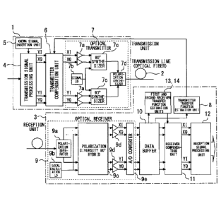
compensation means that the
number of taps of the filter is set to one, and only polarization rotation is
performed without
compensating band characteristics of the optical transceiver by the block
(common 2 x 2 MIMO
filter with plurality of taps compensates band characteristics).
CA 03047882 2019-06-20
- 20 -
[0051]
Further, the transmitter transfer function estimation unit 8 processes each of
the X-
polarized wave and the Y-polarized wave as the complex vector signal as with
the first receiver
transfer function estimation unit 13 in Fig. 4; however, the transmitter
transfer function
estimation unit 8 can independently process each of the lanes XI, XQ, YI, and
YQ. In this case,
the delay difference among the lanes can be extracted and compensated. When
the X-polarized
wave is processed as the complex vector signal, the delay difference (Skew)
between the lanes XI
and XQ is regarded as zero. In the case where the delay difference is not
ignorable, it is
necessary to perform extraction and compensation of the transfer function for
each lane. This is
true of the Y-polarized wave.
[0052]
Fig. 14 is a flowchart to acquire the transfer function or the inverse
transfer function of
the optical transmitter according to the embodiment of the present invention.
First, the known
signal is input to an input of the transmission signal processing unit 4, and
an optical modulation
signal is transmitted from the optical transmitter 7 (step S201). At this
time, the transmitter
compensation unit 6 is bypassed. Note that the transmitter compensation unit 6
can include the
configuration same as the configuration of the receiver compensation unit 11
illustrated in Figs. 5
to 8. Next, the reception data is acquired by the data buffer 10 on the
reception side (step S202).
Next, the transmitter transfer function estimation unit 8 acquires the digital
data from the data
buffer 10 (step S203). The known signal synchronization unit 8a extracts the
known signal from
the acquired digital data. The various transmission characteristic
compensation and the optical
receiver compensation are performed on the extracted known signal. The optical
receiver
compensation is performed with use of the temporary inverse transfer function
of the optical
receiver 9 estimated in step SI. Although Fig. 13 illustrates the
configuration in which the
receiver compensation unit 11 on the post-stage of the data buffer 10 performs
compensation with
use of the temporary inverse transfer function, the compensation is not
particularly necessary for
the above-described processing of the transmitter transfer function estimation
unit 8.
[0053]
The known signal that has been subjected to the various transmission
characteristic
compensation and the optical receiver compensation still includes influence of
the transfer
function of the optical transmitter 7. Accordingly, the FIR filter 8d set with
the inverse
CA 03047882 2019-06-20
-21 -
characteristics thereof is applied as the adaptive filter to the signal to
correct the inverse
characteristics again so as to minimize a square of difference between the
output and the known
signal. The filter coefficients of the FIR filter 8d configuring the adaptive
filter can be
determined as the time response of the inverse transfer function through the
processing. The
method of determining the inverse transfer function is generally known as
Wiener solution or the
LMS algorithm described below.
[Math. 4]
e(n) = s(n) - y(n) = s(n) - h(n)Tx(n)
h(n) = [x(n)rx(n)]-1x(n)Ts(n) Wiener Solution
h(n + 1) = h(n) + e(n)x(n) LMS
where s(n) is the known signal, y(n) is the output of the adaptive filter,
e(n) is the difference
between the known signal s(n) and the output y(n) of the adaptive filter, and
h(n) is the time
response of the adaptive filter.
[0054]
In the above-described example, the inverse transfer function of the optical
transmitter 7
can be directly determined by the adaptive equalization circuit. Therefore,
step S203 and step
S204 can be integrally processed. In contrast, in the case where the transfer
function of the
optical transmitter 7 is determined once, the inverse transfer function is
calculated (step S204).
[0055]
Next, the estimated inverse transfer function of the optical transmitter 7 is
set to the
transmitter compensation unit 6 (step S205). The setting method is the same as
the method
described in step S105. At this time, as described above, each of the lanes
XI, XQ, YI, and YQ
can be independently processed. In this case, the delay difference among the
lanes can be
extracted and compensated.
[0056]
The transfer function or the inverse transfer function of the optical
transmitter 7 can be
determined by the transmitter transfer function estimation unit 8 in the above-
described manner.
Fig. 15 is a diagram illustrating the time response of the inverse transfer
function of the optical
transmitter determined by the transmitter transfer function estimation unit.
Fig. 16 is a diagram
illustrating the frequency response (amplitude characteristics and phase
characteristics) of the
CA 03047882 2019-06-20
- 22 -
inverse transfer function of the optical transmitter determined by the
transmitter transfer function
estimation unit.
[0057]
Fig. 17 is a diagram illustrating a second receiver transfer function
estimation unit
according to the embodiment 1 of the present invention. The second receiver
transfer function
estimation unit 14 includes a known signal synchronization unit 14a, a circuit
14b that simulates
distortion in transmission for chromatic dispersion compensation, frequency
offset compensation,
polarization dispersion/polarization rotation addition, clock phase addition,
phase noise addition,
and the like, an FIR filter I4c for adaptive equalization, and a square error
minimization circuit
14d. The known signal synchronization unit 14a has a function to extract the
known signal from
the digital data, and estimates, by various kinds of estimation blocks,
addition data to be set to the
circuit that simulates the distortion on the post-stage from the state of the
extracted known signal.
In other words, estimation of the transfer function or the inverse transfer
function of the optical
receiver 9 includes processing to estimate the transmission characteristics of
the transmission line
2. Note
that the order of the units in the circuit 14b that simulates distortion in
transmission for
chromatic dispersion compensation, frequency offset compensation, polarization
dispersion/polarization rotation addition, clock phase addition, phase noise
addition, and the like
may be changed.
[0058]
The second receiver transfer function estimation unit 14 processes each of the
X-polarized
wave and the Y-polarized wave as the complex vector signal as with the first
receiver transfer
function estimation unit 13 in Fig. 14; however, the second receiver transfer
function estimation
unit 14 can independently process each of the lanes XI, XQ, YI, and YQ. In
this case, the delay
difference among the lanes can be extracted and compensated. When the X-
polarized wave is
processed as the complex vector signal, the delay difference between the lanes
XI and XQ is
regarded as zero. In the case where the delay difference is not ignorable, it
is necessary to
perform extraction and compensation of the transfer function for each lane.
This is true of the
Y-polarized wave.
[0059]
Fig. 18 is a flowchart to estimate the true transfer function or the true
inverse transfer
function of the optical receiver according to the embodiment of the present
invention. First, the
CA 03047882 2019-06-20
-23 -
known signal is input to the input of the transmission signal processing unit
4, and the optical
modulation signal is transmitted from the optical transmitter 7 of the
transmission unit 1 to the
reception unit 3 (step S301). At this time, the inverse transfer function of
the optical transmitter
7 estimated in step S2 of Fig. 2 is set to the transmitter compensation unit 6
to compensate the
transmission characteristics of the optical transmitter 7. Note that the
transmitter compensation
unit 6 can include the configuration same as the configuration of the receiver
compensation unit
11 illustrated in Fig. 5.
[0060]
Next, the reception data is acquired by the data buffer 10 on the reception
side (step S302).
The second receiver transfer function estimation unit 14 acquires the digital
data from the data
buffer 10 (step S303). The known signal synchronization unit 14a extracts the
known signal
from the acquired digital data. The extracted known signal is supplied to the
FIR filter 14c as
the adaptive filter. On the other hand, chromatic dispersion, frequency
offset, polarization
dispersion/polarization rotation, clock phase, and phase noise that are
estimated as the
transmission line distortion are added to the known signal, and the resultant
signal is compared
with the output of the adaptive filter. An addition amount of each of the
chromatic dispersion,
the frequency offset, the polarization dispersion/polarization rotation, the
clock phase, and the
phase noise is estimated by the various estimation blocks from the state of
the known signal.
[0061]
At this time, the transfer function of the optical transmitter 7 is regarded
to have been
compensated by the transmitter compensation unit 6 at the output of the
adaptive filter. When
the transfer function of the optical receiver 9 is compensated by the adaptive
filter, the output of
the adaptive filter is influenced only by the transmission line distortion.
The signal is compared
with the known signal added with the transmission line distortion, and
difference therebetween
(square error) is minimized. As a result, the filter coefficients of the FIR
filter 14c as the
adaptive filter can be determined as time response of the inverse transfer
function of the optical
receiver 9. The method of determining the inverse transfer function is
generally known as
Wiener solution or the LMS algorism described below.
[Math. 5]
e(n) = d(n) - y(n) = d(n) - h(n)Tx(n)
h(n) = [x(n)Tx(n)]-Ix(n)Td(n) Wiener Solution
CA 03047882 2019-06-20
- 24 -
h(n + 1) = h(n) + iLt e(n)x(n) LMS
where d(n) is the known signal, y(n) is the output of the adaptive filter,
e(n) is the difference
between the known signal d(n) and the output y(n) of the adaptive filter, and
h(n) is the time
response of the adaptive filter.
[0062]
In the above-described example, the true inverse transfer function of the
optical
transmitter 7 can be directly determined by the adaptive equalization circuit.
Therefore, step
S303 and step S304 can be integrally processed. In contrast, in the case where
the true transfer
function of the optical receiver 9 is determined, the true inverse transfer
function is calculated
from the transfer function (step S304).
[0063]
Next, the estimated true inverse transfer function of the optical receiver 9
is set to the
receiver compensation unit 11 (step S305). The setting method is the same as
the method
described in step S105. At this time, as described above, each of the lanes
XI, XQ, YI, and YQ
can be independently processed. In this case, the delay difference among the
lanes can be
extracted and compensated.
[0064]
The true transfer function or the true inverse transfer function of the
optical receiver 9 can
be determined by the second receiver transfer function estimation unit 14 in
the above-described
manner. Fig. 19 is a diagram illustrating the time response of the inverse
transfer function of the
optical receiver determined by the second receiver transfer function
estimation unit. Fig. 20 is a
diagram illustrating the frequency response (amplitude characteristics and
phase characteristics)
of the inverse transfer function of the optical receiver determined by the
second receiver transfer
function estimation unit.
[0065]
Fig. 21 is a diagram illustrating a second receiver transfer function
estimation unit
according to the embodiment 2 of the present invention. Unlike the embodiment
1 illustrated in
Fig. 13, the transmitter compensation unit 6 is bypassed in step S301
illustrated in Fig. 18, and
the transmission line distortion and the transfer function of the optical
transmitter 7 are added to
the known signal in step S303. The other processing is the same as the
processing according to
the embodiment 1. In the present embodiment, setting on the transmission side
is unnecessary.
CA 03047882 2019-06-20
- 25 -
Therefore, the transfer function or the inverse transfer function of the
optical transmitter 7 and the
transfer function and the inverse transfer function of the optical receiver 9
can be estimated only
by calculation on the reception side. In this case, these estimation
calculation can be
implemented by a single device. In particular, these estimation calculation
can be easily
implemented by a PC including an interface to take in the digital data of the
data buffer 10.
[0066]
Fig. 22 is a frequency spectrum after the compensation by the optical
transmission
characteristic compensation method according to the embodiment of the present
invention. In a
case where the compensation of the optical transceiver is not performed, both
shoulders of the
spectrum drop due to the frequency band characteristics of the optical
transmitter 7. In contrast,
in the case where the compensation is performed only on the transmission side
without separating
the reception-side frequency characteristics, both shoulders of the frequency
characteristics of the
optical receiver 9 rise as a result. Further, in a case where the compensation
is individually
performed on the optical transmitter 7 side and on the optical receiver 9
side, an ideal rectangular
spectrum can be confirmed. In the optical transmission, noise (flat in band)
by the optical
amplifier is dominant. Therefore, influence of noise enhancement can be
avoided in the case
where the optical spectrum has the ideal shape (rectangle in this case). As
described above, in
order to suppress influence of the noise enhancement, it is important that the
transfer function of
the optical transmitter 7 is compensated on the optical transmitter 7 side and
the transfer function
of the optical receiver 9 is compensated on the optical receiver 9 side. This
can be achieved by
the embodiment according to the present invention.
[0067]
Fig. 23 is a diagram illustrating Q-value improvement effect after the
compensation by
the optical transmission characteristic compensation method according to the
embodiment of the
present invention. The Q value is an index indicating error rate. The higher Q
value is
obtainable as the error rate is lower. An OSNR is an optical signal-to-noise
ratio. As with the
spectrum illustrated in Fig. 22, an improvement amount of the Q value to the
wide OSNR is
larger in the case where the compensation is individually performed on the
optical transmitter 7
side and the optical receiver 9 side also in this case.
[0068]
CA 03047882 2019-06-20
- 26 -
As described above, according to the present embodiment, the transfer function
or the
inverse transfer function of the optical transmitter 7 and the transfer
function or the inverse
transfer function of the optical receiver 9 can be estimated. In other words,
it is possible to
estimate the transmission characteristics of each of the optical transmitter 7
and the optical
receiver 9. The transfer functions or the inverse transfer functions are set
to the transmitter
compensation unit 6 and the receiver compensation unit 11, which makes it
possible to
individually compensate the transfer function of the optical transmitter 7 and
the transfer function
of the optical receiver 9. As a result, the transmission characteristics of
each of the optical
transmitter 7 and the optical receiver 9 can be compensated, which makes it
possible to obtain
optimum transmission characteristics as illustrated in Fig. 22 and Fig. 23.
Further, the optical
transmission characteristic estimation method, the optical transmission
characteristic
compensation method, the optical transmission characteristic estimation
system, and the optical
transmission characteristic compensation system according to the present
embodiment are easily
implemented by a PC or the like, which is useful as a calibration system in
optical
communication.
[0069]
Further, in the present embodiment, the transmission unit 1 and the reception
unit 3 are
connected, the temporary transfer function or the temporary inverse transfer
function of the
optical receiver 9 of the reception unit 3 is determined, the transfer
function or the inverse
transfer function of the optical transmitter 7 in the transmission unit 1 is
determined with use of
the temporary transfer function or the temporary inverse transfer function of
the optical receiver 9,
and the true transfer function or the true inverse transfer function of the
optical receiver 9 is
finally determined. In a case where the transfer function or the inverse
transfer function of one
of the optical transmitter 7 and the optical receiver 9 is previously acquired
or calibrated, however,
the transfer function or the inverse transfer function of the other of the
optical transmitter 7 and
the optical receiver 9 can be estimated from the digital data in the reception
unit 3 when the
known signal is transmitted from the transmission unit 1 to the reception unit
3 and the transfer
function or the inverse transfer function previously acquired or calibrated.
In this case, the
transfer function or the inverse transfer function of each of a plurality of
apparatuses can be
determined by sequentially changing only the apparatus side including an
unknown transfer
function. These methods are also included in the technical idea of the present
invention.
CA 03047882 2019-06-20
- 27 -
[0070]
Further, step S2 and step S3 illustrated in the flowchart of Fig. 2 may be
repeated two or
more times with use of the true transfer function or the true inverse transfer
function of the optical
receiver 9 estimated in step S3 as the temporary transfer function or the
temporary inverse
transfer function of the optical receiver 9 in step S2. This makes it possible
to estimate the
transfer function or the inverse transfer function of the optical transceiver
with higher accuracy.
This is also included in the technical idea of the present invention.
Reference Signs List
[0071]
1 transmission unit; 2 transmission line; 3 reception unit; 6 transmitter
compensation unit; 7
optical transmitter; 8 transmitter transfer function estimation unit; 9
optical receiver; 11 receiver
compensation unit; 13 first receiver transfer function estimation unit; 14
second receiver transfer
function estimation unit