Note: Descriptions are shown in the official language in which they were submitted.
CA 03050062 2019-07-12
WO 2017/123416
PCT/US2016/068922
TITLE: MOLECULAR SENSORS AND RELATED METHODS
INVENTORS: BARRY MERRIMAN; PAUL MOLA; CHULMIN CHOI
CROSS-REFERENCE TO RELATED APPLICATIONS
[0001]
This application claims priority to U.S. Provisional Patent Application No.
62/278,889 filed on January 14, 2016, entitled "MANUFACTURE OF MOLECULAR
BRIDGES FOR NANOSCALE DEVICES"; U.S. Provisional Patent Application No.
62/278,900 filed on January 14, 2016 entitled "METHODS FOR MANUFACTURE OF
BEADS ON A SUBSTRATE FOR NANOSCALE DEVICES"; and U.S. Provisional Patent
Application No. 62/278,907 filed on January 14, 2016 entitled "METHODS OF
NUCLEIC
ACID ANALYSIS USING MOLECULAR ELECTRONICS SENSORS, the disclosures of
which are incorporated herein by reference.
FIELD
[0002] The
present disclosure relates to electronic sensor devices. In particular, the
disclosure relates to electronic sensor devices that comprise one or more
biomolecule
components in a measurement circuit, and can be used for nucleic acid
sequencing.
BACKGROUND
[0003]
Measuring properties at the molecular scale presents numerous challenges, due
to
the sensitivity required, and the presence of many potential sources of noise.
In describing
sensors for this purpose, it is therefore helpful to be clear about all
sources of measurement
error. In general, for any system or object that may be measured, a measured
state, m, will
only be an approximation of the actual system state, a. This may be due to any
of a number
of factors, such as imperfect signal interpretation reflecting error due to
the operation of the
sensor, the readout process, or the signal interpretation, and also because
contacting the
sensor to the system in some cases may perturb the state of the system. That
the measured
state m is different than the actual state a reflects the measurement error of
the combined
sensor, readout, and interpretation. Ideally, a sensor system will be
constructed to make this
measurement error as small as possible.
[0004] To
measure states at a molecular scale, such as in the case of sequencing a DNA
molecule, various efforts have been directed to create sensor systems in which
the sensor
device has a "probe" that contacts the molecules of interest, preferably on a
single-molecule
scale, while other features of the sensor device are on larger nano- or micro-
scales for
1
CA 03050062 2019-07-12
WO 2017/123416
PCT/US2016/068922
purposes of manufacturing the sensor devices or integrating them into a signal
transduction
system.
[0005] In
particular, a biosensor is an analytical device that functionally integrates a
biological recognition component into a signal transduction system, to measure
properties of
biologically relevant molecules, such as DNA, RNA or proteins. That
integration provides
rapid and convenient conversion of biological events to detectable electrical
signals. Of the
various electrical biosensing architectures that have been devised, systems
based on field-
effect transistors (FETs) appear promising because they can directly translate
interactions
between target molecules (e.g., biological molecules) and the FET surface into
detectable
.. electrical signals. In a typical FET device, current flows along a channel
that is connected to
two electrodes (also referred to as the source and the drain). The channel
conductance
between the source and the drain can be modulated by a third electrode (also
referred to as
the gate) that is coupled to the channel through a thin dielectric insulating
layer. FETs can be
used to detect target chemicals and measure chemical concentrations for a wide
range of
commercial applications. A classical and widely used example is a FET-based pH
sensor,
used to measure hydrogen ion concentration. This was introduced by Bergveld in
the 1970's,
and is used in solid-state pH sensors. The general field of ion-sensitive FET
(ISFET) devices
expands upon that concept for other chemical concentration measurements.
[0006] A
limitation of current FET-type biosensor systems is their sensitivity. Current
biosensor systems are unable to perform single molecule detection and
identification.
Likewise, they are unable to monitor single molecule reaction dynamics. These
sensitivity
limitations of FET-type biosensors prevent their use as detectors in important
biochemical
assays, such as in single molecule sequencing reactions.
[0007]
Some efforts to improve FET biosensor sensitivity have focused on use of
carbon
.. nanostructures, such as carbon nanotubes, to form the channel between
electrodes. However,
carbon nanostructures pose various obstacles with respect to biosensor
functionalization. In
particular, there is no way to engineer in attachments sites at specific,
desired atomic
locations, for the purpose of attaching functional or sensitizing probe
molecules.
Additionally, present limits on precision, control, and scale of the synthesis
of carbon
.. nanostructures pose further challenges with respect to sensitivity and
reliable production of
individual sensors, establishing high density scalable arrays of sensors, and
commercial
viability of sensor manufacturing. Current carbon nanotube synthesis methods
typically
produce structures on a scale of around 100 nm or longer in length, a scale
that is likely to
2
CA 03050062 2019-07-12
WO 2017/123416
PCT/US2016/068922
pose limitations with respect to sensitivity as well as sensor density on a
multi-sensor
platform.
[0008]
Thus, molecular-scale electronic biosensor devices with architectures
compatible
with increased sensitivity and precision, reliable engineering, and that are
further compatible
with efficient and commercially-viable manufacturing methods for achieving
increased
sensor density on a multi-sensor platform, are desirable. Likewise, improved
methods of
manufacturing such sensor devices are also desirable.
SUMMARY
[0009] The
present disclosure generally relates to sensors, systems including the
sensors,
and to methods of forming and using the sensors and systems. Exemplary sensors
can be
used to, for example, sequence molecules such as DNA, RNA, or other
oligonucleotides.
While the ways in which various embodiments of the disclosure address the
drawbacks of the
prior art sensors are discussed in more detail below, in general, the
disclosure provides
sensors that are relatively easy and inexpensive to manufacture.
[0010] In various embodiments of the present disclosure, a sensor
comprises: a source
electrode; a drain electrode spaced apart from the source electrode by a
sensor gap; a gate
electrode, wherein the source, drain and gate electrode cooperate to form an
electrode circuit;
and a bridge molecule bridging across said sensor gap, connecting the source
and drain
electrodes; and a probe coupled to the bridge molecule, wherein interaction of
the probe with
a nucleic acid is detectible by monitoring at least one parameter of the
electrode circuit. In
various examples, the nucleic acid comprises DNA or RNA, or variants thereof
[0011] In
various embodiments, the probe of the sensor comprises an enzyme, such as,
for example, a DNA polymerase, a reverse transcriptase, an exonuclease, or a
helicase. In
some cases, the probe may comprise a DNA polymerase, such as, for example,
Phi29, Poll,
or a mutant thereof
[0012] In
various embodiments, the bridge molecule may comprise an antibody, double-
stranded DNA or a protein alpha-helix. For example, the antibody may comprise
an IgG
antibody, such as an IgG antibody that recognizes at least one contact point
on the source or
drain electrode or that recognizes contact points on the source and drain
electrodes. Other
bridge molecules may include a nucleic acid duplex, such as, for example, a
DNA duplex, a
DNA-RNA hybrid duplex, a DNA-PNA hybrid duplex, a PNA-PNA duplex, or a DNA-LNA
hybrid duplex.
3
CA 03050062 2019-07-12
WO 2017/123416
PCT/US2016/068922
[0013] In
accordance with various embodiments of the disclosure, a sensor includes a
first contact coupled to a first electrode, a second contact coupled to a
second electrode, a
sensor gap defined between one of the first contact and the first electrode
and one of the
second contact and the second electrode, and a bridge molecule comprising a
first end and a
.. second end, wherein the bridge molecule is coupled to the first contact at
the first end and
coupled to the second contact at the second end. In accordance with various
aspects of these
embodiments, the bridge molecule is a biopolymer, or the bridge molecule is
chemically
synthesized. In accordance with additional aspects, the sensor includes a
third or gate
electrode. In these cases, the gate electrode can be used to tune and/or
activate the sensor
device. In accordance with further aspects, the sensor gap has a sensor gap
dimension of
between about 5 nm and about 30 nm. In accordance with additional aspects, the
first end or
the bridge molecule comprises a first self-assembling anchor; in accordance
with further
aspects, the second end comprises a second self-assembling anchor. Exemplary
bridge
molecules can include one or more of the following attributes: the bridge
molecule can be
linear (e.g., a linear biopolymer), the bridge molecule has an end-to-end
length that is less
than a persistence length of the bridge molecule, and the bridge molecule
includes an end-to-
end length configured to approximate the dimension of the sensor gap.
Exemplary bridge
molecules include a nucleic acid duplex, such as, for example, a DNA duplex, a
DNA-RNA
hybrid duplex, a DNA-PNA hybrid duplex, a PNA-PNA duplex, or a DNA-LNA hybrid
duplex. Exemplary sensors include a probe attached to the bridge molecule. The
probe can
be configured to engage a single target molecule. Exemplary probes can include
or be an
enzyme configured to engage the target molecule during a reaction in a
solution.
[0014] In
accordance with additional embodiments of the disclosure, a sensor includes a
first electrode overlying a substrate surface, a second electrode overlying a
substrate surface,
.. a sensor gap defined between the first electrode and the second electrode
(or between
contacts attached to the electrodes), and a bridge molecule comprising a first
end and a
second end, wherein the bridge molecule is coupled to a first contact at the
first end and
coupled to a second contact at the second end. The sensor gap can include a
sensor gap
dimension of between about 5 nm and about 30 nm. In accordance with various
aspects of
these embodiments, the bridge molecule is a biopolymer, or the bridge molecule
is
chemically synthesized. In accordance with additional aspects, the sensor
includes a third or
gate electrode. In these cases, the gate electrode can be used to tune and/or
activate the
sensor device. In accordance with additional aspects, the first end or the
bridge molecule
comprises a first self-assembling anchor; in accordance with further aspects,
the second end
4
CA 03050062 2019-07-12
WO 2017/123416
PCT/US2016/068922
comprises a second self-assembling anchor. Exemplary bridge molecules can
include one or
more attributes noted herein. Exemplary bridge molecules include a nucleic
acid duplex,
such as, for example, a DNA duplex, a DNA-RNA hybrid duplex, a DNA-PNA hybrid
duplex, a PNA-PNA duplex, or a DNA-LNA hybrid duplex. Exemplary sensors
include a
probe attached to the bridge molecule. Exemplary sensors include a probe
attached to the
bridge molecule. The probe can be configured to engage a single target
molecule.
Exemplary probes can include or be an enzyme configured to engage the target
molecule
during a reaction in a solution.
[0015] In
accordance with additional exemplary embodiments, a system includes a sensor
as described herein. The system can additionally include one or more circuits,
such as a
circuit formed using a substrate used to form the sensor or upon which the
sensor resides.
Systems can additionally or alternatively include additional circuits and/or
devices to, for
example, remove noise from a signal and/or assist with interpretation of the
signal.
[0016] In
accordance with yet additional embodiments of the disclosure, a method
includes providing a sensor, such as a sensor described herein; contacting a
nucleic acid
template with a polymerase, wherein the polymerase is coupled to a bridge
molecule
comprising a portion of a sensor; providing a nucleotide base mix; performing,
by the
polymerase, an incorporation event comprising incorporation of a nucleotide
from the
nucleotide base mix into a synthesized nucleic acid; and detecting a signal
produced by the
.. incorporation event. In accordance with various aspects of these
embodiments, a method can
additionally include a step of applying an electrical potential to the
sensor¨e.g., to tune or
activate the sensor. In accordance with further aspects, noise can be removed
from the signal.
[0017] In
accordance with yet additional embodiments, a method of manufacturing a
biomolecular sensing device includes the steps of forming a first electrode
and a second
.. electrode on a substrate surface, wherein the first electrode and the
second electrode are
separated by an electrode gap; placing a first contact on the first electrode
and a second
contact on the second electrode, wherein the first contact and the second
contact are separated
by a contact gap; and attaching a bridge molecule to the first contact and the
second contact.
Exemplary methods can further include the step of contacting the bridge
molecule with a
probe to couple the probe to the bridge molecule.
[0018]
And, in accordance with further embodiments of the disclosure, a method of
sequencing an oligonucleotide comprises using one or more sensors as described
herein.
5
CA 03050062 2019-07-12
WO 2017/123416
PCT/US2016/068922
BRIEF DESCRIPTION OF THE DRAWINGS
[0019] The
subject matter of the present disclosure is particularly pointed out and
distinctly claimed in the concluding portion of the specification. A more
complete
understanding of the present disclosure, however, may best be obtained by
referring to the
detailed description and claims when considered in connection with the drawing
figures.
[0020]
FIG. 1 illustrates a schematic representation of a sensor in accordance with
various embodiments;
[0021]
FIGS. 2A and 2B illustrate views of a sensor device in accordance with various
embodiments;
[0022]
FIG. 3 illustrates a profile view of a portion of a sensor in accordance with
various
embodiments;
[0023]
FIG. 4 illustrates a sensor comprising a biopolymer bridge molecule in
accordance
with various embodiments;
[0024] FIG. 5 illustrates a sensor comprising a biopolymer bridge molecule
in accordance
with various embodiments;
[0025]
FIGS. 6A and 6B illustrate views of a sensor device in accordance with various
embodiments;
[0026]
FIG. 7 illustrates a signal trace before and after noise removal in accordance
with
various embodiments;
[0027]
FIG. 8 illustrates a process flow for a method of fabricating electrodes using
CMOS techniques in accordance with various embodiments;
[0028]
FIG. 9 illustrates a process flow for a method of fabricating contacts using
CMOS
techniques in accordance with various embodiments;
[0029] FIG. 10 illustrates a process flow for a method of fabricating
contacts using
CMOS techniques and deposition of preformed contact particles in accordance
with various
embodiments;
[0030]
FIGS. 11A-11C illustrate views of a sensor device fabricated using CMOS
techniques in accordance with various embodiments;
[0031] FIG. 12 illustrates a scanning electron micrograph of a contact
array following
biopolymer bridge self-assembly in accordance with various embodiments;
[0032]
FIG. 13 illustrates a signal trace produced during a biopolymer bridge self-
assembly event for a sensor in accordance with various embodiments;
6
CA 03050062 2019-07-12
WO 2017/123416
PCT/US2016/068922
[0033]
FIG. 14 illustrates a signal trace produced during a process of probe binding
to a
biopolymer bridge of a sensor in accordance with various embodiments;
[0034]
FIG. 15 illustrates a signal trace produced during template binding to a probe
in
accordance with various embodiments;
[0035] FIG. 16 illustrates a signal trace produce during template-dependent
base
incorporation by a probe in accordance with various embodiments;
[0036]
FIG. 17 illustrates a signal trace produced by a single template-dependent
base
incorporation event by a sensor in accordance with various embodiments;
[0037]
FIG. 18 illustrates signal traces produced by a sensor in accordance with
various
embodiments under various experimental conditions;
[0038]
FIG. 19 illustrates a signal traces produced by a sensor in accordance with
various
embodiments under various conditions in response to a target comprising
unmodified and 5-
methylcytosine modified nucleotides;
[0039]
FIG. 20 illustrates signal traces produced by a sensor in accordance with
various
embodiments in response to a long template sequence under various experimental
conditions;
[0040]
FIG. 21 illustrates a chemically synthesized bridge molecule in accordance
with
various embodiments;
[0041]
FIG. 22 illustrates the general self-assembly process wherein a molecular
circuit
element, such as a biopolymer, bonds within a target location in the circuit
to both the
positive and negative electrodes bridging them to form an assembled molecular
circuit;
[0042]
FIG. 23 illustrates the use of a material contact point in circuit self-
assembly. The
contact point, shown as "A," is a spatially localized, precisely positioned
material element
that can guide precise self-assembly, and provide electrical or mechanical
connection. The
basic steps of adding a contact point and attaching the molecular element are
shown on the
left. How this can result in a desired circuit is indicated at right. The
group "B" is a conjugate
group on the bridging molecule that can selectively bind to the contact point;
[0043]
FIG. 24 illustrates use of an additional contact group "C" to specifically
bind in
additional molecular components "D" represented as an ellipse, with conjugate
binding site
"E" to the primary bridge molecule, in a series of assembly steps;
[0044] FIG. 25 illustrates how spikes in electrical current relate to each
steps in the self-
assembly of a sensor device;
[0045]
FIG. 26 is a diagrammatic representation of ideal images of bridged contacts
(green box) and un-bridged contacts (red box);
7
CA 03050062 2019-07-12
WO 2017/123416
PCT/US2016/068922
[0046] FIG. 27 is an electron microscope image of a substrate after
bridging reactions and
labeling reactions. Green squares highlight contacts having a well formed
bridge;
[0047] FIG. 28 is an image of higher efficiency 20 nm double-stranded DNA
bridge-
binding to an array of gold contact points. Bridges are labeled with a small
gold dot for
imaging purposes. Green squares highlight examples of well-formed bridges.
Higher levels of
binding to gold contact points, and bridge, due to deposition in a high salt
buffer solution
(bridge reaction conditions: 1 [tM bridge concentration incubated with binding
array for 1
hour in a 5X TBS buffer);
[0048] FIG. 29 is an image of alpha-helix peptide bridge binding to test
array of gold dot
contact points;
[0049] FIG. 30 is an image of IgG antibody bridge binding;
[0050] FIG. 31 illustrates a schematic of test set-up for electrical
measurements on bridge
molecules;
[0051] FIG. 32 illustrates a plot of current vs time showing three spikes
indicative of
bridge-electrode binding events;
[0052] FIG. 33 is an EM image of labeled bridges;
[0053] FIG. 34 is an EM image of dSDNA bridging of gold electrodes;
[0054] FIG. 35 illustrates the steps of process (1) used to manufacture a
small bead at a
desired location. Beginning from the upper left in the figure, a layer of
resist (grey) is
pattered on a substrate (blue), with an open disk of diameter D. Then a layer
of adhesive
(green) is deposited into the disk. Then a solution of pre-made beads,
fabricated by standard
means is exposed to this, where the beads have diameter d such that steric
hindrance allows
only one bead per adhesive disk. After removal of resist, what remains is a
bead of diameter
d, positioned near the center of the adhesive disk, but of a size smaller that
the disk diameter
D;
[0055] FIG. 36 illustrates the steps of process (1) for establishing a
small bead from FIG.
35, shown in 3D perspective and overhead views. Starting from a substrate,
standard
patterning and deposition methods are used to deposit an adhesive disk of
material of
diameter D into a pattern rendered in a resist coating (grey). Exposure to
beads and removal
of resist results in a bead attached to the adhesive patch, and steric
hindrance allows for only
one bead per adhesive disk. Thus, this process established a bead in a desired
location, with a
diameter smaller than what is dictated by the patterning process. In
particular, this allows
manufacture of contact points at resolution exceeding that of the patterning
method;
8
CA 03050062 2019-07-12
WO 2017/123416
PCT/US2016/068922
[0056]
FIG. 37 illustrates the steps of process (2) embodiment (a): Beginning from
the
upper left, deposition of a rectangle of bead material (gold) of width W on a
suitable substrate
(blue), which, upon annealing, and under the action of surface tension, breaks
up into a line
of beads. Then, a protective layer of removable resist (red) is patterned and
deposited,
protecting region that would contain a single bead. The remaining beads are
removed, and
then the resist is removed, leaving a single bead near a preferred end of the
original rectangle
of material;
[0057]
FIG. 38 illustrates an alternative embodiment, b, of process (2), where, in
contrast
to that shown in FIG. 37, the final deposited layer (red) is used to cover the
un-wanted beads,
leaving only the bead at the preferred end exposed and available for use in
the greater nano
device;
[0058]
FIG. 39A illustrates an example of one preferred embodiment of process (2),
wherein the patterning method used is e-beam lithography, and the goal is to
make beads at
the proximal ends of two electrode strips. The illustration depicts the
process through the
point of breaking up the rectangular layers into beads, and prior to final
steps to achieve a
single bead at a preferred end of each rectangle;
[0059]
FIG. 39B is an electron microscopy image showing the process of FIG. 39A
reduced to practice on a substrate that consists of elevated and depressed
substrate ridges,
onto which the gold layer is deposited and allowed to break up into beads. The
image shows
that the beads are substantially smaller in diameter than the underlying width
of the
rectangular strips, and the narrowed (depressed) strips are small enough that
a single line of
beads form;
[0060]
FIG. 40 illustrates bead formation process (3), in which a rectangular pattern
is
produced, and deposition of an adhesion material 1 (blue), followed by
material 2 (gold),
followed by an interfacial layer, such as oxidation induced by a vacuum break,
(grey), to
establishing the uppermost left configuration. Then (arrow) material 3 is
deposited in a thin
layer (shown as gold again), which may be the same material as 2, then (arrow)
a protective
layer (red) is patterned and deposited, such as silicon oxide, leaving exposed
a small region
of a preferred end. Then (arrow) annealing is performed, which causes the
small patch of
material 3 bounded by the protective layer and interfacial layer to break off
and bead up,
forming a bead of material 3 of smaller diameter than and of the primary
patterning
dimensions, located at the end of the rectangular region;
[0061]
FIG. 41 illustrates an array of beads produced using the processes (1) or (2).
In the
case of process (1), the initial patterning and material deposition processes
can be used to
9
CA 03050062 2019-07-12
WO 2017/123416
PCT/US2016/068922
create an array of adhesive material disks on the substrate (original
footprints indicated by
dashed circles), The process will then deposit the preformed beads shown.
Alternatively, if
method (2) is used, entire columns of beads can be established with a single
protection step,
based on an array of deposited initial material rectangles;
[0062] FIG. 42 illustrates the use of the bead-up process in order to
produce nano-contact
points for an array of molecular electronics devices. The array of beads are
positioned such
that each pair of electrodes receives a pair of beads as contact points,
positioned near the ends
of the electrodes;
[0063] FIG. 43 shows electron microscope images of gold beads deposited
on an
adherent surface. Beads are gold nanoparticles approximately 5 nm to 10 nm in
diameter;
[0064] FIG. 44 shows electron microscope images of a control sample
comprising gold
beads adherent to un-derivatized silicon surface;
[0065] FIG. 45 shows Atomic Force Microscope (AFM) images of gold beads
deposited
on a derivatized adherent surface. Beads are gold nanoparticles approximately
5 nm to 10 nm
in diameter;
[0066] FIG. 46A shows the plate map, setting forth the various
concentrations of gold
nanoparticles deposited into wells, with triplicate columnar repeats of
buffer, affinity
antibodies, naïve serum, and control non-specific mouse IgG, at various
dilutions indicated in
rows;
[0067] FIG. 46B is a color coded intensity map of final readings from the
ELISA plate;
[0068] FIG. 46C is the corresponding table of numeric ELISA readings;
[0069] FIG. 46D depicts the final data results summarized in graphical
form, showing
that the antibody with specific affinity has greater binding than the surface
beads than various
controls, across the entire range of bead concentrations deposited on the
surface;
[0070] FIG. 47 illustrates one preferred form of a molecular electronics
circuit for
measuring DNA sequence. An enzyme is coupled between source and drain
electrodes, to
form a circuit that includes a meter for measuring an electrical property,
such as current under
applied source-drain and gate voltages, or a similar system properties (such
as voltage at
constant applied current). The measured property S(t) as a time trace reflects
the underlying
sequence of the DNA, due to the processive action of the enzyme on DNA, and
its variable
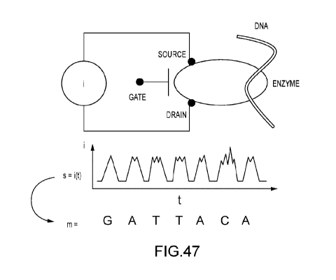
properties as an electrical component during this processing;
[0071] FIG. 48 sets forth ccommonly occurring methylated forms of nucleic
acid bases.
When these are present in DNA, it is desirable to be able to read out their
presence in the
sequence as well, as this may have biological relevance;
CA 03050062 2019-07-12
WO 2017/123416
PCT/US2016/068922
[0072] FIG. 49 illustrates FIG. 1 in a more standard source-drain-gate
geometry;
[0073] FIG. 50 illustrates a schematic of another preferred form of a
molecular
electronics circuit for measuring DNA sequence. An enzyme is coupled as a
secondary
element to a primary conducting element between source and drain electrodes,
to form a
circuit in which the enzyme may provide gating function as well as conduction.
The circuit
includes a meter for measuring an electrical property, such as current under
applied source-
drain and gate voltages, or similar system properties (such as voltage at
constant applied
current). The measured property S(t) as a time trace reflects the underlying
sequence of the
DNA, due to the processive action of the enzyme on DNA, and its variable
properties as an
electrical component during this processing;
[0074] FIG. 51 depicts the schematic of FIG. 1 in a more descriptive
preferred
embodiment with a source-drain-gate geometry from semiconductor devices, and a
molecular
bridge between electrodes as the primary conduting element, and a coupling
point or
conjugation group that couples the enzyme to the bridge, as one means of
ensuring proximity,
and potentially electrical connection;
[0075] FIG. 52 illustrates a preferred embodiment wherein the enzyme
comprises
polymerase, which is extending a primed single stranded DNA template, assuming
a suitable
buffer is present that contains dNTPs. The incorporation process
(incorporation of A
nucleotide shown) produces a corresponding identifiable feature in the
measured current
trace, thereby determining sequence;
[0076] FIG. 53 illustrates an embodiment of sequencing when there is a
detectable signal
of incorporation, indicated as a signal spike in the measured circuit
parameter, such as
current, i. Trial flows of single nucleotide types, A, C, G, T, are performed,
separated by
wash steps (timing of nucleotide flows and washes indicated by letters and
underscores on the
time axis), and the resulting observed signal spikes determine sequence as
indicated. Note
that homopolymer sequence series, such as "TT", are indicated as multiple
incorporation
spikes during the corresponding trial flow. Shown is the result of flowing the
A base, in a
situation in which A is incorporated and produces a signal spike, and
corresponding next base
of the resulting DNA sequence;
[0077] FIG. 54 depicts use of modified nucleotides to produce detectible
signals.
Indicated is a case where each dNTP carries a modification group (indicated as
red balls) that
have detectible influence on the current the incorporation process. Such a
modification could
be on the cleavable gamma phosphate, and therefore removed by the polymerase,
or could be
cleavable in a separate cleavage reaction, performed after a sensing reaction.
Shown is the
11
CA 03050062 2019-07-12
WO 2017/123416
PCT/US2016/068922
instance in which a modified A base in incorporated. The concept is
illustrated here with the
four different modification groups represented as four different numbers of
attached balls
(G:1, A:2, T:3, C:4), resulting in enhancing the traces to have the same
number of minor
spikes within the trace for each nucleotide;
[0078] FIG. 55 depicts use of a modified nucleotide to enhance
incorporation signal in
the embodiment of sequencing when there is a detectible signal of
incorporation used in a
trial flow method. Indicated is a case where each dNTP carries a modification
group
(indicated as red ball) that has detectible influence on the current in the
incorporation process.
Such a modification could be on the cleavable gamma phosphate, and therefore
removed by
the polymerase, or could be cleavable in a separate cleavage reaction,
performed after a
sensing reaction. Shown is the A step of the trial flow process, where the A
is the correct base
for incorporation;
[0079]
FIG. 56 illustrates kinetic encoding of sequence information. The time between
incorporation spikes indicated the base being incorporated, here do to
difference in dNTP
concentrations indicates: A is at the lowest concentration, therefore a long
time between
spikes indicates the waiting time expected for A incorporation, while G is at
the highest
concentration, so that the shortest time between spikes indicates a G
incorporation (first
interval);
[0080]
FIG. 57 illustrates a preferred embodiment of the bridge, which is a helical
polymer (dsDNA or protein alpha helix) coupled to gold contacts via a thiol
linkage
(thiolated nucleotides in DNA ends, or cysteine placed at alpha helix
termini), and with a
specifically synthesized internal biotin, for coupling to streptavaidin
conjugated to an
enzyme;
[0081]
FIG. 58 illustrates another preferred embodiment of the bridge, as an IgG
protein
(native or engineered) with specific affinity to contact points on the
electrode (affinity to
primary contact point material, or antigen derivatization of surface), with
coupling via IgG
specific binding proteins (such as anti-IgG antibody, or Protein A or Protein
G) that is
otherwise conjugated to the protein of interest, or the protein of interest
could be directly
conjugated to the IgG, using native or engineered conjugation sites;
[0082] FIG. 59 illustrates combination of partial sequence information from
replicate
sequencing of the same (or replicated) DNA templates using different
embodiments of the
methods described, to achieve complete information. Blue traces indicate
partial information
from each separate instance, relative to the grey trace of combined
information (which is not
directly observable in a single sequencing run). Indicated here, a template is
sequenced (left
12
CA 03050062 2019-07-12
WO 2017/123416
PCT/US2016/068922
embodiment) to produce partial information (shown, only A bases can be
detected), and again
(right embodiment, indicating a change to the bridge and the enzyme), to
produce
complementary or auxiliary sequencing information (shown, G, T, C are
detected), which is
then combined to obtain complete sequence. The two sequencing embodiments
could be
physically or temporally isolated and independent, using replicate templates,
or could be
different states of the same sensor system at different times¨perhaps produced
by a buffer
change, temperature change or change in applied voltages such as gate
voltage¨re-reading
the same template. Any number of such complementary embodiments could have
their
information combined to improve the final sequence determination;
[0083] FIG. 60 illustrates an embodiment wherein the enzyme is an
exonuclease. Signals
are produced by the effect of enzyme conformation, DNA conformation, and freed
nucleotides, on circuit parameters;
[0084]
FIG. 61 illustrates an embodiment wherein where the processive enzyme is a
DNA helicase, unwinding a double stranded DNA template;
[0085] FIG. 62 illustrates an embodiment wherein where the enzyme is a
complex
formed of a protein nanopore and motor protein enzyme having DNA translocation
capability;
[0086]
FIG. 63 illustrates an integrated chip sensor array device. This format
provides a
way to perform massively parallel sensing of sequence from many sequences at
the same
time, as well as the option of deploying diverse or identical sensor
constructs at each site, for
robust averaging or data integration of sequence data for replicates of a
single DNAS
fragment;
[0087]
FIG. 64A illustrates a trial run in the terminator sequencing process. In the
presence of a mixture of dNTPs (blue) and dideoxy terminators, ddNTPs
(purple),
polymerization and sensing proceeds, producing incorporation spikes used to
count base
position (to position 8 shown) as indicated, until a terminator is randomly
incorporated. At
the end of the reaction, a sensing measurement takes place, to identify the
terminator base (in
this case, A). Thus the underlying sequence has A at position 8. By repeating
such
measurements on this template, or replicate templates, and combining the
information, the
complete sequence of bases at all locations along the template can be
determined;
[0088]
FIG. 64B illustrates an Alternative embodiment of terminator sequencing, where
only a single base terminator, in the case shown, A dideoxy termination
(ddATP, purple), is
used in a given reaction. In this mode, when the reaction terminates, it is
implied that the base
in question is A, the terminator, and the count of the number of incorporation
spikes gives the
13
CA 03050062 2019-07-12
WO 2017/123416
PCT/US2016/068922
position of this A in the template. Repeating many runs for A with replicate
templates will
randomly determine all A locations in the template, and performing similar
series of runs for
the other terminator bases C, G, T, respectively, will determine the
respective locations of all
these bases in the template, thereby determining the entire sequence;
[0089] FIG. 64C illustrates an embodiment embodiment of terminator
sequencing, where
a replicated template of interest is loaded into each chip indicated, and all
A termination data
is accumulated from one run on a parallel sensor array, indicated in the top
series, and
similarly for the C-, G-, and T- termination reactions, and the single base
results from each
are accumulated (red arrow) to determine the full sequence of the template in
question;
[0090] FIG. 65 illustrates use of a DNA hybridization probe in the
molecular sensor, in
place of an attached enzyme, and the detection of hybridization by monitoring
a circuit
parameter such as current. Hybridization is indicated by a different current
level. One
preferred embodiment would couple the DNA hybridization probe, to a
streptavidin (orange
group), via a biotinylated base located in the probe. This form of probe and
detection
measurement supports sequencing by hybridization, which is based on
aggregating many
such measures, using a set of informative probes, against replicated template
molecules;
[0091]
FIG. 66 illustrates alternative embodiments of incorporating a hybridization
probe
into the sensor, wherein the probe forms all or part of the bridge molecule.
In a preferred
embodiment, the DNA containing the probe would be coupled to the contact
points using
gold-thiol linkage, with gold contact points and thiolated nucleotides in the
DNA. The figure
illustrates three different ways such a hybridization probe could be
configured as all or part of
a DNA bridge molecule. In the lower instance, the probe could further
partially hybridize to
the underlying DNA, to set up competitive hybridization with the target for
added stringency;
[0092]
FIG. 67 illustrates one example of enhancing the primary hybridization signal,
by
using enzymatic extension (3' extendible end of the probe indicated by blue
arrow) to
incorporate one or more bases, perhaps including detectible groups (purple) to
enhance the
signal. Such enzymatic extension both adds stringency / checks for proper
pairing, as well as
the means of enhancing the electronic sensor signal, as indicated by the three
levels in the
current plot (no hybridization, hybridization, extension product present). In
the case of single
base extension, if the base identity is detectible (either from the four dNTPs
together, or
through a series of individual dNTP extension trials) it can also add one more
base of
sequence information, enhancing the sequencing capacity of the method;
[0093]
FIG. 68 illustrates a sensor enclosed in microwells or nanowells that can be
sealed
and unsealed in a bulk / macroscopic process. This localizes reactants and
reaction products,
14
CA 03050062 2019-07-12
WO 2017/123416
PCT/US2016/068922
to facilitate other modes of detection. This may also benefit from multiple
sensor types per
well, or multiple probe molecules per sensor, so that a processive enzyme can
be present with
a probe to detect a reaction product;
[0094]
FIG, 69 illustrates details of the bridge and probe molecule structure
typically
used for experimental work. The bridge in this case is double stranded DNA
molecule, of 20
nm length shown (60 bases), with thiol groups at both 5' ends for coupling to
gold contacts
on a metal electrode;
[0095]
FIG. 70 illustrates a schematic of a test set-up for electrical measurements
on
molecular sensors is shown. In the upper portion of FIG. 70, a cross-section
of the electrode-
substrate structure and attachment to an analyzer for applying voltages and
measuring
currents through the bridge molecule is shown. In the lower portion of FIG.
70, a perspective
view of an electrode array for bridging circuits is illustrated;
[0096]
FIG. 71A is an electron microscope image of an array of titanium electrodes
with
gold metal dot contacts for bridge binding. Electrodes are on a silicon
substrate and were
produced by e-beam lithography;
[0097]
FIG. 71B is an electron microscope close-up image of one of the electrode gaps
in
FIG. 71A, showing an electrode gap of 7 mm and a gold dot contact gap of 15 mm
gold-to-
gold spacing;
[0098]
FIG. 71C is an electron microscope close-up image of a single electrode gap
from
FIG. 71B, showing approximately 10 nm diameter gold dots at the tips of the
two electrodes;
[0099]
FIG. 72 illustrates electrode test chip architecture. In this case, the
electrode array
was formed on a 1 cm silicon substrate, using e-beam lithography. The series
of three SEM
images in FIG. 72 shows the 20 electrode pairs at increasing resolution, down
to the 10 nm
scale of the electrode gap;
[00100] FIG. 73 illustrates an embodiment of the sensor device wherein a
silicon oxide
passivation layer is used to protect electrodes from solution. The openings in
passivation
expose the electrode area on the nm scale, and the electrical contact pads on
a 10 micron
scale;
[00101] FIG. 74 illustrates an embodiment of a flow cell to support controlled
exposure of
liquid solutions to the sensor chip surface. The flow cell is molded PDMS
polymer;
[00102] FIG. 75 illustrates a chip mounted in a chip carrier for electrical
measurements;
[00103] FIG. 76 illustrates conductivity of an assembled sensor complex,
showing
measured Current-versus-Voltage (I-V) Characteristics of DNA bridge molecules
and
complete sensor complexes (bridge with polymerase) in wet (dilute salt buffer)
and dry (air)
CA 03050062 2019-07-12
WO 2017/123416
PCT/US2016/068922
conditions, along with controls of open circuit electrodes in air, water and
dilute salt buffer.
The figure shows that the bridge and sensor complex conduct on the order of
100 mpico-Amp
currents at 1 Volt of applied source-drain voltage. Measurements are done on
semiconductor
parameter analyzer via an SMU;
[00104] FIG. 77 illustrates electronic monitoring of a molecular sensor self-
assembly onto
gold-dot contact electrodes. Current versus time measurements are used to
monitor assembly
of bridge and molecular sensor complex. Upper left: Phase 1: double stranded
DNA bridge
assembles with thiol groups on 5' ends assembles onto electrode gold contact
point, as
indicated by jump in current. Upper right: Phase 2: polymerase-streptavidin
complex binds to
biotinylated site on the dsDNA bridge, as indicated by jump up in current.
Lower right: Phase
3: primed single-stranded DNA template binds to polymerase to complete the
complex, as
indicated by spike in current versus time;
[00105] FIG. 78 shows electron microscope images of a final assembly structure
at two
levels of magnification. In the close-up image, the bridge-complex is visible
without any
labeling, seen as the blurry high contrast region joining the electrodes
(pointed to by the
green arrow);
[00106]
FIG. 79 are four plots measuring incorporation signals with the sensor,
illustrating
measuring incorporation signals with the sensor, and shows the current signals
resulting from
the sensor being supplied with various primed, single stranded DNA sequencing
templates
and dNTPs for incorporation and polymerization. In each case, the major signal
spikes
represent signals from discrete incorporation events, wherein the polymerase
enzyme adds
another base to the extending strand. Upper left: template is 20 T bases;
upper right, template
is 20 G bases; lower left, template is 20 A bases; lower right, template is 20
C bases. The
approximate rate of incorporation observed is 10-20 bases per second,
consistent with
standard enzyme kinetics, except for the lower rate of ¨1 base per second due
to rate limiting
factors (e.g. lower dNTP concentration);
[00107] FIG. 80 illustrates a close up of the signal produced from a single
base
incorporation event. The signal has a double-peak structure which could
potentially be used
to help characterize the identity of the base, in addition to detecting the
incorporation event;
[00108] FIG. 81 illustrates an embodiment of sensing methylated bases. This
figure shows
the potential use of the sensor to sense the methylation state or individual
methylated bases in
the template. The figure shows different signals result from un-methylated
versus methylated
portion of the template (green trace). Higher signal results from the un-
methylated portion,
rather than methylated portion. The experiment shown consists of measuring
traces for a
16
CA 03050062 2019-07-12
WO 2017/123416
PCT/US2016/068922
series of different solution additions onto the sensor chip as indicated, for
the template
sequence indicated. The dCTP flow produced a single base incorporation spike,
and the
addition of dGTP then enabled incorporation to proceed across the CG tract of
the template,
highlighting a difference in signal from methylated versus un-methylated
template;
[00109] FIG. 82 illustrates the long reads capability of the sensor. This
figure shows the
potential to read or analyze long DNA fragments, which is important for
applications where
long range continuity of the data is important, such as de novo assembly of
whole genome
sequences. The DNA template is the 5.4kb PhiX viral genome. At left:
differential signals
from a low-time-resolution read of the template (dNTP mix), versus a follow on
control
(terminator ddNTP mix, polymerase activity blocked) without polymerization. At
right: SEM
image of the electrodes with the long template DNA visible;
[00110] FIG. 83A illustrates an embodiment of a sensor comprising a peptide
alpha-helix
bridge molecule. The bridge molecule in one specific preferred embodiment
reduced to
practice comprises a peptide having a 66 amino acid sequence;
[00111] FIG. 83B illustrates an embodiment of a fully assembled sensor
comprising an
alpha-helix bridge coupled to a neutravidin molecule via the known biotin-
neutravidin
binding reaction, and also the polymerase attached via an additional biotin-
maleimide linker
that has been conjugated to a surface cysteine on the polymerase via the known
maleimide-
cysteine covalent coupling reaction;
[00112] FIG. 84A illustrates a modified C nucleotide used in EXAMPLE 9 (as a
mixture
with dCP4-Cy7 depicted in FIG 84B) in order to enhance signals from the
polymerase
incorporations;
[00113] FIG. 84B illustrates a modified C nucleotide used in EXAMPLE 9 (as a
mixture
with dCP4-lactose depicted in FIG 84A) in order to enhance signals from the
polymerase
incorporations;
[00114] FIG. 85A depicts data from s Sequence Sensing Experiment with the
alpha-helix
peptide bridge. The plot is Current-vs-Voltage traces for the electrodes on a
test chip that has
been incubated with the peptide bridge molecule for 1 hour in PBS buffer, at 1
[tM peptide
concentration, in order to attach bridge to gold contacts. The highest current
trace, which
achieves a 3 nano-amp current at 2 volts applied source-drain, indicates an
electrode with a
bridge molecule in place;
[00115] FIG. 85B depicts additional data from s Sequence Sensing Experiment
with the
alpha-helix peptide bridge. The plot is Current-vs-Time trace showing the
signature of the
subsequent neutravidin binding to the bridge, at time of approximately 10
seconds to 50
17
CA 03050062 2019-07-12
WO 2017/123416
PCT/US2016/068922
seconds, when bridged sensor is exposed to a neutravidin solution with applied
source-drain
voltage of 2 volts;
[00116] FIG. 85C depicts additional data from s Sequence Sensing Experiment
with the
alpha-helix peptide bridge. The plot is Current-vs-Time trace showing the
signature of the
polymerase-maleimide-biotin binding the neutravidin-bridge complex, at the
time of 10-20
seconds, when the latter is exposed to a solution of the former; and
[00117] FIG. 85D depicts additional data from s Sequence Sensing Experiment
with the
alpha-helix peptide bridge. The plot sets forth the resulting sequencing
signals when the
assembled sensor is provided with solution containing a template DNA, with
sequence
having a series of GT repeats: (10xGT) TTT (10x GT) AAA (10x GT) CCC (10x GT).
Figure is annotated with one possible interpretation of these signals, where
major spikes
corresponding to the GT repeat tracts of the template, and overall three
different template
DNA molecules engage with the sensor during the 45 seconds shown.
DETAILED DESCRIPTION
[00118] The detailed description of exemplary embodiments herein makes
reference to the
accompanying drawings, which show exemplary embodiments by way of illustration
and
their best mode. While these exemplary embodiments are described in sufficient
detail to
enable those skilled in the art to practice the invention, it should be
understood that other
embodiments may be realized and that logical, chemical, and mechanical changes
may be
made without departing from the spirit and scope of the inventions. Thus, the
detailed
description herein is presented for purposes of illustration only and not of
limitation. For
example, unless otherwise noted, the steps recited in any of the method or
process
descriptions may be executed in any order and are not necessarily limited to
the order
presented. Furthermore, any reference to singular includes plural embodiments,
and any
reference to more than one component or step may include a singular embodiment
or step.
Also, any reference to attached, fixed, connected or the like may include
permanent,
removable, temporary, partial, full and/or any other possible attachment
option. Additionally,
any reference to without contact (or similar phrases) may also include reduced
contact or
minimal contact.
[00119] In various embodiments, a single molecule biosensor device can
comprise a first
electrode and a second electrode. The first electrode and the second electrode
are separated
by a sensor gap defined by the electrodes and/or contacts attached to the
electrodes. The first
and second electrodes can be coupled by a bridge molecule spanning the sensor
gap. The
18
CA 03050062 2019-07-12
WO 2017/123416
PCT/US2016/068922
bridge molecule can comprise a biopolymer, such as nucleic acid or amino acid
polymers.
The bridge may also comprise a chemically synthesized molecule, which may
include a
synthetic organic molecule, a polymer comprising synthetic analogs of
biopolymer
monomers, or other wholly synthetic monomers not derived from a biological
molecule. The
differences between a "biopolymer" and a "chemically synthesized molecule" is
not meant to
be so strictly literal as to exclude the possibility for synthetic
transformations that modify an
otherwise natural biopolymer into a useful bridge molecule, such as, for
example,
synthetically modifying the 3' and 5' ends of an otherwise naturally occurring
polynucleic
acid sequence for subsequent binding and bridging. A bridge molecule, whether
comprised
of a biopolymer or a synthetic molecule, may have a known, atomically precise
molecular
structure. The bridge molecule attachment to the electrodes may be mediated by
a contact. A
probe molecule or molecular complex can be coupled to the bridge molecule. The
probe can
be a biomolecule such as an enzyme configured to interact with a single target
molecule. In
various embodiments, a sensor device can comprise multiple single molecule
biosensors
arrayed in parallel. Such multi-sensor devices can be used to perform parallel
detection,
discrimination, and/or characterization or identification of multiple
individual target
molecules in a complex mixture of target and other molecules.
[00120] FIG. 1 illustrates a schematic representation of a sensor device 100
comprising a
sensor 101 in accordance with various embodiments. Sensor 101 includes a first
electrode
102 and a second electrode 103. Sensor 101 may also include a gate 104, as
described in
greater detail below. Sensor 101 can further comprise a sensor complex 105
functionally
coupled to the first electrode 102 and the second electrode 103. In various
embodiments, the
sensor complex may be coupled to the electrodes via first contact 106 and
second contact 107
attached to the respective electrodes.
Sensor complex 105 can comprise multiple
components, such as a bridge molecule and a probe molecule, as described in
greater detail
below. Sensor complex 105 can interact with the surrounding environment,
thereby enabling
sensor 101 to perform a sensing function. For example, as illustrated in FIG.
1, sensor
complex 105 may interact with a target molecule 108 such as a DNA molecule,
and the
sensor device can be used to detect the presence of and/or properties of the
target molecule.
[00121] In various embodiments, sensor device 100 and sensor 101 may be
operatively
connected to circuit 120 to detect a change of an electrical property of
sensor 101. Circuit
120 is preferably an integrated circuit with micro-scale proximity to the
sensor 101, but
circuit 120 could also be embodied as an external electrical meter, such as a
bench-top
current meter. Sensor device 100 can comprise a plurality of sensors 101.
Integrated circuit
19
CA 03050062 2019-07-12
WO 2017/123416
PCT/US2016/068922
120 can comprise a circuit architecture that may be fabricated using CMOS
fabrication
methods. Integrated circuit 120 can comprise an electronic measurement circuit
for each
sensor 101 that is fabricated within the same chip that provides support for
the sensor.
Expressed differently, a sensor device 100 can comprise a sensor 101 and an
integrated
circuit 120 in an integrated microcircuit. Integrated circuit 120 can further
comprise readout
circuitry and input/output features for connection to an external signal
processing system 121.
[00122] In various embodiments, use of an integrated circuit 120 residing on a
common
semiconductor chip with sensor 101 can reduce sources of electronic noise in
readings that
can be produced by macroscopic, external circuit elements. For example, such a
circuit may
be a mixed signal CMOS sensor, comprising a small number of transistors, in
the range of 1
to 200 depending on the performance requirements for sensitivity and readout.
Such a circuit
can function to measure current in a single sensor 101 in various embodiments.
Further, a
sensor device 100 can comprise an integrated circuit 120 comprising
sensor/readout circuits
for an array of sensors 101 so as to support the simultaneous operation of a
large number of
sensors in contact with the same sample.
[00123] In various embodiments, a sample contacted by a sensor 101 will
comprise a
liquid-phase sample. The solution comprising the sample may be extremely
dilute and at low
ionic strength to reduce the noise in electrical measurements performed using
the sensor. The
acquired signal will typically be the current flowing between electrodes 102
and 103 in the
sensor, although it could be a related observable electronic parameter such as
the voltage
between electrodes, resistance/conductance between electrodes, or gate
voltage.
[00124] In various embodiments, the configuration of sensor 101 and integrated
circuit
120 in an integrated microchip chip format amenable to fabrication using
modern CMOS
fabrication methods can facilitate production of sensor devices with a highly
compact
architecture. In various embodiments, the integrated circuit for a sensor may
be located
within about 100 p.m of the sensor gap, or within about 50 [tm of the sensor
gap, or within
about 20 [tm of the sensor gap, or within about 10 [tm of the sensor gap, or
within about 5 [tm
of the sensor gap, or within about 1 [tm of the sensor gap. Moreover, in
various
embodiments, a sensor device can comprise a plurality of sensors, each sensor
having an
associated integrated circuit located within the parameters specified above.
[00125]
Signal processing system 121 can be configured to provide electronic control
of
sensor device 100 and to receive, store, and analyze signal received from the
sensor device
and each sensor 101 therein. Signal processing system 121 can comprise a
computer system
with a processor and/or software configured to perform the electronic control
functions,
CA 03050062 2019-07-12
WO 2017/123416
PCT/US2016/068922
including control of the voltage and current applied to each sensor 101, and
to perform the
signal processing functions for signal received from each sensor 101.
[00126] For example and as illustrated in FIG. 1, a sensor device 100
comprising a sensor
101 may be used to perform a nucleic acid sequencing reaction. During
operation of the
device, a voltage may be applied between the first electrode and the second
electrode of
sensor 101, with interactions of the sensor with a target producing modulation
of current flow
through a biopolymer bridge molecule (see, e.g., 333, FIG. 3) that can be
measured using
integrated circuit 120 and signal processing system 121. Sensor 101 may
produce a signal
pattern 122 over time t with signal features 123 produced by the sensor in
response to the
sensor complex interaction with features of target molecule 108. Signal
processing system
121 can receive and process the signal pattern and provide a sequence output
124 in response
to the signal pattern, which in this context is the interpretation of the
signal.
[00127] In various embodiments, a single molecule biosensor can take the form
of a
transistor, such as a field effect transistor (FET), with the attached bridge
molecule and/or
probe, and/or target molecule and/or solution-phase molecules in close
proximity to these
components, serving as a channel or conductive path in an electrical circuit.
In such an
embodiment, a sensor complex comprising a single probe molecule may be
configured to
bind or interact with a single target molecule as explained in greater detail
below, thereby
providing the biosensor with single molecule sensitivity. Such a transistor
embodiment may
include a two or three terminal transistor, or potentially more terminals,
such as in the case of
multi-gate devices.
[00128] FIGS. 2A and 2B illustrate views of a sensor device 200 in accordance
with
various embodiments. Sensor complexes are not shown in the illustrated views
of sensor
device 200. Sensor device 200 comprises a plurality of sensors 201, with each
sensor
comprising a first electrode 202 and a second electrode 203. Each sensor can
further
comprise a sensor gap 239. In the illustrated embodiment, each sensor
comprises a first
contact 206 attached to the first electrode and a second contact 207 attached
to the second
electrode. In various embodiments, the electrodes can be disposed on a
semiconductor
substrate surface. For example, sensor device 200 can comprise a silicon
nitride layer 260
overlying a silicon dioxide layer 261. Sensor device 200 can further comprise
buried gate
204 underlying the semiconductor substrate layer(s) on which the electrodes
are disposed.
The various components described above can be fabricated on a support such as
a silicon chip
263. As illustrated schematically in FIG. 2A, each of the first electrode 201,
the second
electrode 202, and the gate 204 may be connected to a signal processing system
221, which
21
CA 03050062 2019-07-12
WO 2017/123416
PCT/US2016/068922
may be an external meter, as depicted in the illustration, but which could
alternatively be
integrated circuitry (details not shown).
[00129] With reference now to FIG. 3, a profile view of a portion of a sensor
301 and
sensor complex 305 are illustrated in greater detail. Sensor 301 comprises
first electrode 302
and second electrode 303. First electrode 302 and second electrode 303 may be
disposed on
a substrate 320. In various embodiments, sensor 301 can further comprise a
first contact 306
and a second contact 307 operatively coupled to first electrode 302 and second
electrode 303,
respectively. However, contacts are not strictly required, and a sensor in
accordance with the
present disclosure need not comprise a first and second contact. The ends of
first electrode
302 and second electrode 303 define an electrode gap 330. Likewise, for a
sensor comprising
contacts such as sensor 301, the distance between first contact 306 and second
contact 307
defines a contact gap 331. The actual dimension of a contact gap for any given
first contact
and second contact may vary dependent on the configuration of the contact and
the point of
the contact used for reference. For example, for the hemispherical first
contact 306 and
second contact 307 illustrated in FIG. 3, the dimension of contact gap 331 may
be measured
between the nearest points of the contact or from center to center. In various
embodiments,
one of the electrode gap and the contact gap, or the gap defined collectively
or by various
combinations of the electrodes and/or contacts, may be referred to as a sensor
gap.
[00130] With continued reference to FIG. 3, sensor 301 further comprises
sensor complex
305. In various embodiments, a sensor complex 305 can comprise a bridge
molecule 333 and
a probe 334. Probe 334 can be coupled to bridge molecule 333 via a linker 337,
which here
is shown as a streptavidin-biotin complex, with the biotin covalently
incorporated into a
nucleotide of the DNA bridge 333, and the streptavidin chemically, covalently
cross-linked to
the polymerase 334. Each of the various components of sensor complex 305 are
described in
greater detail below.
[00131] In various embodiments, a bridge molecule 333 can comprise a
chemically
synthesized bridge molecule or a biopolymer bridge molecule. A chemically
synthesized
bridge molecule or a biopolymer bridge molecule may be configured to span a
sensor gap
both structurally and functionally. For example, a chemically synthesized
molecule or
biopolymer molecule may be configured through selection and use of atomically
precise
molecular subunits (e.g., monomeric units for incorporation into a polymeric
bridge
molecule) that provide for construction of a bridge molecule with known or
predictable
structural parameters, incorporation of features that facilitate self-assembly
to contact points
22
CA 03050062 2019-07-12
WO 2017/123416
PCT/US2016/068922
and self-assembly of a probe molecule to a bridge molecule, as well as
suitable
electrochemical properties for electrical connection of electrodes.
[00132] A chemically synthesized bridge molecule is a molecule that can be
assembled by
a person of skill in the art of synthetic organic chemistry. For example, a
chemically
synthesized molecule can comprise a polypyrrole, polyaniline, or polythiophene
backbone.
With reference briefly to FIG. 21, an example of a general structure of a poly
thiophene-based
chemically synthesized bridge molecule 2100 is illustrated. Chemically
synthesized bridge
molecule 2100 can comprise a chain of thiophene rings 2101 forming the
backbone of the
bridge molecule, with n1 and n2 thiophene rings on either side of a probe
support moiety 2102
that may be configured at a specific location in the bridge molecule 2100.
Since each
thiophene ring 2101 is approximately 0.3 nm wide, a chemically synthesized
bridge molecule
comprising about 10 to about 100 rings could be constructed to span an about 3
nm to an
about 30 nm gap. The termini (e.g., Al and A2) of a chemically synthesized
bridge molecule
can comprise thiol or amine groups, or other groups configured to bind to
electrode or contact
materials. A chemically synthesized bridge molecule can also be configured
with a linker
(e.g., L) suitable to provide attachment of a probe molecule. Any other
chemically
synthesized bridge molecule configuration, comprised of any suitable backbone
moiety now
known to, or that may be hereinafter devised by, a person of ordinary skill in
the art, may be
used in accordance with various embodiments of the present disclosure.
[00133] As used herein, the term "biopolymer" can include any molecule
comprising at
least one monomeric unit that can be produced by a living organism, although
the actual
monomeric unit comprising a biopolymer or the polymer itself need not be
produced by an
organism and can be synthesized in vitro. Examples of biopolymers include
polynucleotides,
polypeptides, and polysaccharides, including well known forms of these such as
DNA, RNA
and proteins. Bridge molecules that comprise a biopolymer can include multi-
chain
polymeric proteins in a simple "coiled-coil" configuration, as occurs in
collagen proteins, or a
more complex folding of heavy and light chain polymeric proteins, such as in
immunoglobin
molecules (e.g. IgG). Such complexes that comprise biopolymers also include
common
nucleic acid duplex helices, such as a DNA double helix, which is two DNA
single strand
molecules bound into a helical double strand by hydrogen bonding, PNA-PNA
duplexes, as
well as DNA-RNA, DNA-PNA, and DNA-LNA hybrid duplexes. A biopolymer molecule
need not be naturally occurring or produced by an organism to be classified as
a biopolymer.
Instead, for purposes of the present disclosure, the term "biopolymer" can
include molecules
that are synthesized enzymatically as well as non-enzymatically and can
likewise include
23
CA 03050062 2019-07-12
WO 2017/123416
PCT/US2016/068922
molecules comprising synthetic analogues of naturally-occurring monomeric
units. For
example, biopolymers can comprise peptide nucleic acids (PNAs) and locked
nucleic acids
(LNAs), synthetic analogues of DNA and RNA that have enhanced stability
properties. In
addition, a biopolymer can comprise any of a variety of modifications that may
be added to a
molecule. The use of biopolymer bridge molecules can provide various benefits,
including
synthesis of precisely controlled structures having suitable size and
chemistry for sensor
function, they may be naturally compatible with the target molecules for the
sensor (e.g.,
compatible with the same liquid buffer medium), and the biotech industry has
developed
extensive capabilities to design, engineer and synthesize such molecules, and
to manufacture
them economically and with high quality control.
[00134] A bridge molecule can be configured to span a sensor gap and be
coupled to an
electrode and/or a contact on either side of the sensor gap in a manner
suitable to provide
electronic communication between the bridge molecule and the electrode and/or
contact.
[00135] In various embodiments, a bridge molecule can comprise a linear
biopolymer such
.. as a double-stranded DNA helix or an a-helical polypeptide. As illustrated
in FIG. 3, bridge
molecule 333 comprises a linear biopolymer double-stranded DNA bridge molecule
with a
first end 334 coupled to first contact 306 and a second end 335 coupled to
second contact
307.
[00136] In various embodiments, a rigid bridge structure may provide
advantages in terms
of taking on a well-defined configuration during and after assembly of the
sensor complex.
Without wishing to be bound by theory, a linear biopolymer can comprise a semi-
flexible
polymer that may be described by its bending rigidity. On a short length
scale, a linear
biopolymer may behave as a rigid polymer, requiring a strong force to bend the
polymer,
while on a longer scale, the linear biopolymer may be bent or curved more
easily. The
.. characteristic bending length measure within which a linear biopolymer
essentially behaves
as a rigid molecule in a certain set of environmental conditions is referred
to as the
persistence length. The persistence length can depend on the environmental
conditions in
which a bending force is exerted on the polymer, with variables such as the
temperature and
ionic conditions of the surrounding environment affecting the persistence
length. The
persistence length of a linear biopolymer such as double-stranded DNA may be
estimated
based on theoretical modeling or it may be measured empirically for a set of
environmental
conditions corresponding to a predetermined experimental condition in which a
device in
accordance with various embodiments may be used. For example, the persistence
length of
double-stranded DNA has been calculated at about 30 nm to about 80 nm, and the
persistence
24
CA 03050062 2019-07-12
WO 2017/123416
PCT/US2016/068922
length of an a-helical peptide calculated at about 80 nm to about 100 nm in
various
conditions that may approximate the conditions in which a sensor in accordance
with various
embodiments of the present disclosure may be used. Thus, in various
embodiments, a
double-stranded DNA molecule or an a-helical peptide having an end-to-end
length, as
measured along its major axis, of less than the respective persistence length
parameters
described above may behave as an essentially rigid polymer, thereby providing
certain
advantages or benefits with respect to device assembly and performance.
[00137] In various embodiments, use of linear biopolymers comprised of DNA or
amino
acids permits the straightforward construction of nano-scale sensor components
having a
predetermined length based on the monomeric composition (i.e., the primary
structure) of the
biopolymer. Without wishing to be bound by theory, use of a linear biopolymer
with an end-
to-end length of less than the persistence length may enhance the efficiency
of a self-
assembly step during construction of a biomolecular sensing device in
accordance with
various embodiments. Use of such linear biopolymers provides an ability to
maintain the
specifications of a biopolymer bridge molecule within parameters in which
their
micromechanical properties are more predictable than for longer linear
biopolymers that may
bend or fold, thereby reducing the influence of undesirable stochastic
effects, for example,
during bridge molecule synthesis, handling, self-assembly, or sensor
operation. Moreover,
the use of linear biopolymers permits precise specification of the bridge
molecule length to
the sensor gap (i.e., the electrode gap and/or contact gap dimension and
architecture),
providing a further ability to readily test the performance of theoretical
structural models and
device improvements and to make incremental, well-controlled, and empirically-
testable
modifications. In various embodiments, a linear biopolymer bridge molecule may
be
configured to provide a reduced rate of miscoupling of both the first self-
assembling anchor
at the first and the second self-assembling anchor and the second end to one
of the first
contact and the second contact due to the essentially rigid nature of the
linear biopolymer
bridge molecule at the scale used in the sensor device (e.g., an end-to-end
length of between
about 5 nm and about 30 nm). Similarly, a biopolymer bridge molecule may be
configured to
provide a reduced rate of single-end coupling. This may result when the
substantially rigid
bridge molecule, once coupled at a first contact, restricts the second end to
spend more time
in the proximity of the desired second contact point, owing to the spacing of
contacts, thereby
increasing the rate of the desired second coupling reaction.
[00138] As mentioned above, a biopolymer bridge molecule can comprise a double-
stranded DNA molecule. In various embodiments, a double-stranded DNA can
comprise a
CA 03050062 2019-07-12
WO 2017/123416
PCT/US2016/068922
thiol-modified oligo comprising a thiol-modified nucleotide or base. A thiol-
modified
nucleotide can comprise a self-assembling anchor configured to bind to a gold
nanobead or
similar surface contact. In various embodiments, a self-assembling anchor can
comprise a 5'-
thiol modified nucleotide, which can be located at or near the 5' terminus of
an
oligonucleotide. A double-stranded DNA molecule can comprise a complementary
pair of
oligonucleotides, with each oligonucleotide comprising a 5'-thiol modified
nucleotide, such
that the assembled double-stranded DNA comprises a self-assembling anchor
located at both
termini of a double-stranded DNA molecule. For example, in various
embodiments, a
double-stranded DNA molecule can comprises oligonucleotides with the following
sequences:
[00139] 5'-/5ThioMC6-D/TGC GTA CGT ATG TCA TGA ATG GCG CAG ACT GAT
GTC CTA TGA CGT CGC TAC TGC AGT ACT-3' (SEQ ID NO: 1), and
[00140] 5'-/5ThioMC6-D/AGT ACT GCA GTA GCG ACG TCA TAG GAC A/iBiodT/C
AGT CTG CGC CAT TCA TGA CAT ACG TAC GCA-3' (SEQ ID NO: 2), with the
"/5ThioMC6-D/" denoting a 5'-thiol modifier and "/iBiodT/" denoting an
internal biotin-
modified deoxythymidine nucleotide (Integrated DNA Technologies, Inc.,
Coralville, IA).
When annealed to one another, these oligos provide a double-stranded DNA
molecule with a
5'-thiol modified nucleotide located at each end of the molecule as the first
and second self-
assembling anchors.
[00141] A double-stranded DNA molecule bridge can also further comprise a
biotin linker
component to facilitate linking a probe molecule to the bridge with a
complementary avidin-
type linker component. In
various embodiments and as illustrated in the reverse
oligonucleotide sequence described above, a biotin-modified oligonucleotide
can be
incorporated into one of the oligos of a double-stranded DNA molecule bridge.
In various
embodiments, the biotin-modified oligo is an internal modification, such as
via a modified
thymidine residue (biotin-dT). A variety of biotin modification configurations
may be used,
including attachment to thymidine via a C6 spacer, attachment via a
triethyleneglycol spacer,
attachment via a photocleavable spacer arm, dual biotin modifications,
desthiobiotin
modifications, and biotin azide modifications. Other modifications that are
now known to a
person of skill in the art or may be hereinafter devised and may be made to an
oligonucleotide to facilitate linkage to a probe molecule are within the scope
of the present
disclosure. Similarly, other common small molecules with a protein binding
partner, such
digoxigenin, can play a similar role to that of biotin for such purposes of
conjugation to probe
molecules at precisely atomically specified points in the bridge molecule.
26
CA 03050062 2019-07-12
WO 2017/123416
PCT/US2016/068922
[00142] In various embodiments, a peptide biopolymer bridge molecule can
comprise
various configurations and/or features suitable to provide various desirable
bridge molecule
structure and performance characteristics, including electrode or contact
binding
characteristics, structural characteristics, electrical performance
characteristics, and the like.
For example, a peptide biopolymer bridge can comprise an L-cysteine residue at
one or both
of the amino terminus and the carboxyl terminus to serve as a self-assembling
anchor via
thiol-metal binding to specific metal contacts that engage in strong thiol
binding, such as
gold, palladium or platinum. In other embodiments, a biopolymer bridge
molecule can
comprise a peptide with the known capacity to selectively and strongly bind
gold contacts for
purposes of self-assembly and electro-mechanical connection into the circuit.
Specific such
peptides include those with the following amino acid sequences: MHGKTQATSGTIQS
(SEQ ID NO: 3), VSGSSPDS (SEQ ID NO: 4), and LKAHLPPSRLPS (SEQ ID NO: 5).
Other peptides selected for such properties can similarly bind other specific
metal or material
contacts. For example, VPSSGPQDTRTT (SEQ ID NO: 6) is a known aluminum binding
peptide, and MSPHPHPRHHHT (SEQ ID NO: 7) is a known silicon dioxide binding
peptide.
In various other embodiments, a biopolymer bridge molecule can comprise a
peptide
sequence that includes repetitions of an amino acid motif or motifs selected
from one of the
following amino acid sequence motifs known to favor the formation of stable
alpha-helix
conformations, providing for a linear, rigid, conductive bridge: EAAAR (SEQ ID
NO: 8),
EAAAK (SEQ ID NO: 9), EEEERRRR (SEQ ID NO: 10), and EEEEKKKK (SEQ ID NO:
11). Such a peptide biopolymer bridge molecule can also comprise a modified
amino acid
consisting of a lysine residue with a covalently attached biotin to provide a
conjugation point
at a precisely atomically defined location for avidin-based conjugation to
probe molecule
complexes. A modified lysine can replace a standard lysine or arginine residue
in such a
peptide sequence motif, to otherwise maintain or minimally alter the
properties of the alpha-
helix.
[00143] In various embodiments, a biopolymer bridge molecule can have other
configurations. For example and as illustrated in FIG. 4, a biopolymer bridge
molecule 433
can comprise a linear biomolecule that is flexed, folded, or comprises a
certain degree of
secondary structure. In various embodiments, a biopolymer bridge molecule can
further
comprise molecules having tertiary and/or quaternary structure, including
globular proteins,
antibodies, and multi-subunit protein complexes. An example is illustrated in
FIG. 5, in
which the biopolymer bridge molecule 533 comprises an immunoglobin G protein
(IgG). In
27
CA 03050062 2019-07-12
WO 2017/123416
PCT/US2016/068922
the illustrated embodiment, the electrical contacts (506, 507) are gold nano-
particles, and the
IgG has been established with a specific affinity to bind such particles.
[00144]
Similarly to sensor 301, the configurations illustrated in FIG. 4 and FIG. 5
each
comprise a probe (436 and 536, respectively) coupled to the biopolymer bridge
molecules via
linkers (437 and 537, respectively). The illustrated embodiments are intended
to exemplify
the range of possible biopolymer bridge molecule configurations that may be
couple to
electrodes or contacts comprising different materials and configurations,
including different
metallic or non-metallic conducting or semiconducting contacts in different
structural
configurations. In various embodiments, electrodes or contacts may further be
coated,
treated, or derivatized to facilitate bridge assembly and/or attachment using
products such as
InnovaCoat GOLD nanoparticles (Innova Biosciences).
[00145] A probe in accordance with various embodiments can comprise any
suitable
molecule or multicomponent molecular complex. A probe may be selected based on
the
molecule to be detected by the sensor or the biochemical reaction to be
monitored. Various
examples of probes include peptides, proteins, enzymes, nucleic acids,
ribozymes, catalytic
DNAs, and the like. In various embodiments, an enzyme can comprise a lysozyme,
a kinase,
or a polymerase. Any molecule or complex that exhibits a specific change in
physical,
chemical, or electronic configuration in response to binding or processing of
a substrate or
target molecule may be used as a probe in accordance with various embodiments
of the
present disclosure.
[00146] In various embodiments, a probe can comprise an enzyme such as
polymerase or a
reverse transcriptase suitable for interacting with individual DNA or RNA
target molecules.
Enzymes that catalyze the template-dependent incorporation of nucleotide bases
into a
growing oligonucleotide strand undergo conformational changes in response to
sequentially
encountering template strand nucleic acid bases and/or incorporating template-
specified
natural or analog bases (i.e., an incorporation event). Such conformational
changes can
modulate electrical current through a bridge molecule to which the probe is
coupled, thereby
provide a sequence-specific signal pattern in a manner that is dependent on
the template
molecule. As described above, the signal pattern may be detected by a signal
processing
system and translated to a sequence data output. Moreover, the presence of a
modified
nucleotide in a target nucleic acid sequence may produce unique conformational
changes and
corresponding signal features in a signal pattern that can enable a sensor
device and signal
processing system to directly determine, for example, methylation of bases in
a target
sequence on a base-by-base basis. Such a label-free, direct sequencing method
may permit
28
CA 03050062 2019-07-12
WO 2017/123416
PCT/US2016/068922
discrimination of a nucleotide-specific incorporation event in a sequencing
reaction using
nucleotide base mix comprising a mixture of natural and/or analog bases
corresponding to all
four bases of DNA, although a sequencing process comprising sequentially
providing
individual natural or analog bases in a serial and/or cyclic fashion may also
be used. The use
of a reverse transcriptase as the probe molecule can similarly enable the
direct sequencing of
RNA molecules without the need for an intermediate cDNA conversion step.
[00147] In various embodiments and as described briefly above, a probe can be
attached to
the bridge molecule via a self-assembling linker. A self-assembling linker can
comprise any
of a number of structures suitable to attach a first biomolecule to a second
biomolecule. In
various embodiments, a self-assembling linker can comprise a first linker
component and a
second linker component that is complementary to the first linker component.
The first linker
component and the second linker component may be joined by self-assembly to
form an
assembled linker based on an affinity of the first linker component for the
second linker
component. A first linker component can be associated, for example, with a
bridge molecule,
and a second linker component can be associated with a probe. A linker
component
associated with a bridge molecule can be engineered to a specific site in the
bridge molecule,
such that self-assembly of the probe to the bridge produces coupling of the
probe to the
bridge molecule at a predetermined location on the bridge molecule. A linker
component
selected for association with the probe may be configured to minimize
interference between
the probe and a target, both with respect to the size of the linker component
and the position
at which it is conjugated to the probe. In this manner, joining the
complementary first and
second linker components can provide functional attachment of the probe to the
bridge
molecule. A self-assembling linker can comprise a biotin-avidin coupling
mechanism, with
an avidin (or other avidin-like) protein first linker component and a biotin
small molecule
second linker component, which components form a strong non-covalent bond with
one
another. Other avidin-like proteins include streptavidin, rhizavidin,
bradavidin, NeutrAvidin,
other various amino-acid modified forms of avidin or streptavidin, as well as
divalent or
monomeric derivatives of such avidins which retain biotin-binding
functionality. In various
embodiments, for example, a biotin may be conjugated to the bridge molecule
and a
streptavidin conjugated to the probe molecule. A self-assembling linker can
also comprise
the well-known "click-chemistry" mechanisms for bioconjugation. A self-
assembling linker
can also comprise an antigen-antibody coupling, for example with an antigen
present on the
bridge molecule coupling to an antibody conjugated to the probe molecule. A
self-
assembling linker can also comprise, for example, a SpyCatcher peptide first
linker
29
CA 03050062 2019-07-12
WO 2017/123416
PCT/US2016/068922
component and a SpyTag peptide second linker component, with the two
components binding
to form an irreversible covalent bond. Any other self-assembling linker system
in any
configuration now known to, or that may be hereinafter devised by, a person of
ordinary skill
in the art may be used to couple a probe to a bridge molecule.
[00148] In various embodiments, a sensor need not comprise a probe molecule
distinct
from the bridge molecule. Instead, the bridge molecule itself may be
configured to be acted
on by a target molecule. For example, a bridge can comprise a protein binding
site, such as a
kinase binding site, and be used to detect the presence and/or activity of the
corresponding
protein in a sample based on binding of the target protein to the bridge
and/or modification of
the bridge by the target protein.
[00149] With reference now to FIGS. 6A and 6B, perspective views of a
partially-
fabricated sensor device 600 with and without a sensor enclosure are
illustrated. Sensor
device 600 is a three terminal sensor device comprising a buried gate 640.
Device 600
illustrated in FIG. 6A comprises various features of a sensor device that may
be produced
using CMOS fabrication techniques, such as gate 640 underlying substrate 641
and oxide
642, along with first electrodes 602 and second electrodes 603 separated by
electrode gaps
630, and each electrode having an attached contact 606/607. Attachment of the
various
sensor complex components described above, including a bridge molecule and
probe, may be
performed in downstream self-assembly steps. In various embodiments and as
illustrated in
FIG. 6B, sensor device 600 may first be configured with an enclosure 643
configured to
enclose or form a flow cell around sensor gaps 630 prior to completing
assembly of the
sensors by contacting the sensor with a solution comprising the bridge and/or
probe
molecules. Likewise, enclosure 643 may also be used to perform assays such as
sequencing
reactions. Enclosure 643 can be separately formed and attached to a structure
including
device 600.
Biomolecule Detection and Nucleic Acid Base Discrimination
[00150] In various embodiments, a method for detecting the dynamics and
kinetics of a
single molecule sensing device such as device 100 (FIG. 1) is provided. Any
method for
measuring changes in electrical conductance of a sensor 101 comprising a
bridge molecule
can be used to monitor a sensor device described herein. In various
embodiments, a voltage
of less than about 10 V can be applied to a sensor comprising a biomolecular
bridge
molecule, and in various embodiments described in greater detail below, a
voltage of about
0.5 V is applied. The current flowing through the sensor can be measured as a
function of
CA 03050062 2019-07-12
WO 2017/123416
PCT/US2016/068922
time using integrated circuit 120. Target binding and/or processing events by
a probe (i.e.,
enzyme activity in the case of an enzymatic probe) in sensor complex 105 can
produce
changes to the conductivity of the sensor 101, modulating the measured current
to produce a
signal pattern 122 over time t comprising signal features 123. Such events,
and the
associated conformational changes, including structural, chemical, and
electronic changes
(i.e., charge distributions in an enzyme, substrates, and surrounding
solution) can comprise
kinetic features of target binding and processing, with the various events
producing current
fluctuations comprising signal features 123 that can be measured, recorded,
discriminated,
analyzed or stored using signal processing techniques which are known in the
art. The signal
features can comprise any of a range of possible forms, including wavelets
with shapes that
are triangular, sinusoidal, or have any number of Fourier components. For
example, a
polymerase used as a probe in a sensor can provide a polymerase kinetic
signature for each
discrete interaction with a template base (i.e., a target molecule feature)
and/or a template-
dependent nucleotide incorporation (i.e., the polymerase kinetic signature is
template base-
dependent), with a nucleic acid template target comprising a sequence of
target molecule
features at discrete positions in the target molecule (i.e., first, second,
and nth target molecule
features at first, second, and nth target molecule positions), each target
molecule feature
producing a corresponding signal feature during detection by a sensor in
accordance with the
present disclosure. The n target molecule features can correspond to n
consecutive bases of a
single stranded DNA template molecule (i.e., the target) which is processed by
the
polymerase enzyme to sequentially incorporate complementary nucleotides at
these n target
molecule features. The amplitudes, durations, and shapes of a signal pattern
comprising a
series of signal features can encode a target-specific sensor response that
can be analyzed
using signal processing system 121 to compare the signal pattern to a signal
interpretation
map to determine the identity of the target. Increasing the time resolution of
signal detection
and analysis may provide an ability to further resolve kinetic variability,
transitions, and
intermediate states of a probe-target interaction.
[00151]
Since the fidelity of nucleotide incorporation is paramount to accurate
nucleic acid
sequencing, in various embodiments, a method of sequencing may rely on analog
bases that
increase the conformational changes of template-based nucleotide
incorporation, thereby
producing clearer signals, and/or otherwise provide an enhanced ability to
discriminate
incorporation of the analog base, thereby providing for enhanced sequencing
accuracy. Non-
labeled analog bases that can be used to enhance the kinetic or dynamic
discrimination of
template-dependent nucleotide incorporation are well known and can include
modifications
31
CA 03050062 2019-07-12
WO 2017/123416
PCT/US2016/068922
of the purine and pyrimidine bases and the deoxyribose or ribose and phosphate
portions of a
nucleotide. In particular, this can include adding additional groups to the
gamma-phosphate
of the nucleotide, which accepts large and diverse molecular modifications
that are cleaved
off during incorporation and therefore do not permanently impact the growing
strand and its
interaction with the polymerase.
[00152] In various embodiments, a method can provide detection of unmodified
and
modified nucleotide bases in a nucleic acid template sequence. For example, a
method may
be suitable to distinguish a modified template nucleotide, including /V6-
methyladenosine, /V4-
methylcytosine, 5-methylcytosine, 5-hydroxymethylcytosine, 5-formylcytosine,
and 5-
carboxylcytosine bases, as well as damaged template sequence positions such as
abasic sites.
Without wishing to be bound by theory, a DNA polymerase catalyzing
incorporation of a
nucleotide into a complementary nucleic acid strand during a sequencing
reaction may
exhibit differential polymerase kinetics in a manner dependent on the identity
of the
nucleotide in the template strand. Using devices and methods in accordance
with the present
disclosure, the identity of a nucleotide base in a nucleic acid template may
be determined in
near real-time based on detection of an electronic signature corresponding to
the
incorporation event. Unlike other systems and methods that rely on detection
of a
fluorescence signal associated with incorporation of a fluorophore-labeled
nucleotide,
fluorescence-based detection reagents and signal detection devices are not
required, thereby
reducing cost and complexity of the process.
[00153] In various embodiments, a method can comprise removing noise from a
signal
trace. Removing noise can comprise performing signal processing, such as to
remove 60 Hz
line noise. Removing noise from a signal trace can reduce the error of signal
trace
interpretation. An example of a signal trace produced by sequencing a 12-base
nucleic acid
template, before (upper signal trace) and after (lower signal trace) removal
of 60 Hz line
noise from the signal, is illustrated in FIG. 7. Various methods of noise
removal may be
used, depending on the character of such noise, and such methods are well
known to a person
of skill in the art in the field of signal processing.
[00154] In various embodiments, signal processing to determine the sequence of
a target
bound to a sensor may comprise a probabilistic determination of the identity
of the target,
rather than an exact determination of the sequence. The actual sequence of a
target molecule
may be one of a number of possible unique sequences, each possible unique
sequence having
a unique theoretical signal. A determination of the sequence of the target
molecule may
require a comparison of experimentally measured signal with a signal
interpretation map
32
CA 03050062 2019-07-12
WO 2017/123416
PCT/US2016/068922
comprising a database of unique theoretical signals. The signal interpretation
map may be
generated based on a training data set or library produced using known target
sequences,
signal processing based on positive and negative control measurements to
reduce signal
artifact such as noise, blur, drift, and the like, as well as application of
machine learning
and/or statistical methods such as neural networks, clustering, curve fitting,
model fitting,
Bayesian inference, etc.
Manufacturing and Assembly of a Sensor Device
[00155] In various embodiments of the present disclosure, a method of
producing a
molecular biosensor device as described herein is provided. A method of
producing a
molecular biosensor device can comprise a combination of CMOS fabrication
processes and
molecular biology methods. CMOS fabrications processes can comprise high-
resolution
optical lithography methods that are well known in the art and are suitable
for commercial
scale production of integrated circuits, including devices such as FETs. In
various
embodiments, CMOS fabrication processes can be used to produce integrated
circuits
comprising individual sensors having a first electrode and a second electrode
deposited on a
semiconductor base, with the first electrode and the second electrode
separated by a precisely
defined sensor gap. In a preferred embodiment, a nano-electrode, gap and
contact design
would be chosen so as to be manufacturable entirely within CMOS processes. In
particular, if
specific simple geometries are chosen for these elements, they can be
fabricated using the
high resolution optical lithography methods, such as Extreme UV (EUV) and Deep
UV
(DUV) sources, combined with phase-shifting masks, multiple-patterning, and
other
techniques used to achieve highest resolution CMOS fabrication nodes,
including current and
future 16 nm nodes, 14 nm nodes, 10 nm nodes, 7 nm nodes and 5 nm nodes as
embodied by
specific fabrication facilities, such as those at major foundry companies,
(e.g., TSMC or
GlobalFoundries). Such processes have uniquely high resolution for making
certain specific
pattern features, such as straight line segments, straight line cuts, and
circular spots. Use of
these process-specific geometric elements in the design of nano-electrode,
nano-contact,
and/or gap geometries can facilitate fabrication of a sensor device in
accordance with various
embodiments in the associated CMOS process. However, in general the
manufacturing
techniques employed may also comprise non-CMOS process methods, such as e-beam
lithography, nano-imprint lithography, or milling and etching techniques such
as focused ion
beam milling and plasma etching. Molecular biology fabrication methods can
comprise
synthesis of the desired bridge molecules with precise control over the atomic
configuration,
33
CA 03050062 2019-07-12
WO 2017/123416
PCT/US2016/068922
and delivery of solutions of such biomolecules in a liquid phase under
conditions suitable to
permit interaction and coupling of the biomolecules with electronic sensor
components
produced in upstream CMOS or other fabrication method process, and/or with
other
biomolecules, in specifically designed self-assembly reaction processes.
[00156] In various embodiments, a method of manufacturing a sensor device
described
herein can comprise steps that including: manufacturing an integrated circuit
microchip,
fabrication of sensor electrodes and/or contacts, synthesis of a bridge
biomolecule,
assembling the bridge biomolecule to the electrodes and/or contacts, coupling
a probe to the
bridge biomolecule, and enclosing the sensor device in a flow cell. In various
embodiments,
a sensor can comprise a two terminal circuit, or a sensor can comprise a three
terminal circuit
with a gate. In various embodiments, a gate may have a buried gate
configuration; however,
lateral gate and other gate configurations, including finFET structures, may
also be used.
[00157] In various embodiments, an electrode, contact, and/or gate may be
comprised of
conductive metal materials. For example, an electrode, contact, and/or gate
may comprise
aluminum, titanium, chromium, copper, gold, palladium, platinum, and the like.
In various
embodiments, an electrode, contact, and/or gate may comprise semiconductor
materials,
including doped semiconductor materials that may be used to produce n-type and
p-type
semiconductor electrodes. In various embodiments, an electrode and a contact
attached to the
electrode can comprise the same material, and in various other embodiments, a
contact can
.. comprise a material that is different from an electrode to which it is
attached.
[00158] In various embodiments, an electrode may have any suitable structural
configuration. For example, an electrode can comprise a generally rectangular
cross-section,
although other geometric and irregular cross-sectional profiles are possible
and within the
scope of the present disclosure. In various embodiments, an electrode can have
a maximum
.. cross-sectional dimension (i.e., the maximum dimension of the electrode in
a cross-section of
the electrode) of less than about 30 nm, or less than about 25 nm, or less
than about 20 nm, or
less than about 15 nm, or less than about 14 nm, or less than about 13 nm, or
less than about
12 nm, or less than about 11 nm, or less than about 10 nm, or less than about
9 nm, or less
than about 8 nm, or less than about 7 nm, or less than about 6 nm, or less
than about 5 nm, or
less than about 4 nm, or less than about 3 nm.
[00159] Similarly, in various embodiments, a contact may have any suitable
structural
configuration. For example, a contact can comprise a generally semi-spherical
or hemi-
spherical cross-sectional profile, although other geometric and irregular
cross-sectional
profiles are possible and within the scope of the present disclosure. In
various embodiments,
34
CA 03050062 2019-07-12
WO 2017/123416
PCT/US2016/068922
a contact can have a maximum cross-sectional dimension (i.e., the maximum
dimension of
the contact in a cross-section of the contact) of less than about 20 nm, or
less than about 15
nm, or less than about 14 nm, or less than about 13 nm, or less than about 12
nm, or less than
about 11 nm, or less than about 10 nm, or less than about 9 nm, or less than
about 8 nm, or
less than about 7 nm, or less than about 6 nm, or less than about 5 nm, or
less than about 4
nm, or less than about 3 nm.
[00160] In various embodiments, the first electrode and the second electrode
may be
alternately referred to as a source and/or drain, and in various embodiments,
a source and/or
drain can comprise a distinct structural component from an electrode.
.. [00161] A method of manufacturing can comprise using lithography methods to
define a
first electrode location and a second electrode location on the surface of a
substrate. The first
electrode location and the second electrode location may be defined to produce
a precisely
defined electrode gap between them upon completion of electrode fabrication.
Similarly, in
various embodiments, a method of manufacturing can comprise using lithography
methods to
define a first contact position and a second contact position. The first
contact position and
the second contact position may be defined to produce a precisely defined
contact gap
between them upon completion of contact fabrication. Likewise, a contact can
be configured
with a defined structure. Various methods that may be used to manufacture a
biosensor are
described in greater detail below.
[00162] With reference now to FIG. 8, a lithographic method 800 for
fabricating
electrodes is illustrated. In various embodiments, a fabrication method may
begin with a
microchip substrate such as a silicon substrate 880 overlayed with a silicon
oxide layer 881 a
resist layer 882. The resist layer can comprise any suitable resist material
suitable, such as
poly(methyl methacrylate). Adhesion promoters may also be used in a
fabrication process in
accordance with the present disclosure. In the illustrated embodiment, e-beam
lithography is
used to expose the resist layer and to define a first electrode track 883 and
a second electrode
track 884 in the resist layer (step 810). Following the lithography step, the
resist is developed
(step 820) to remove the resist in the areas defined in the lithography step.
Next, a deposition
step (step 830) may be performed to form a first electrode 802 and a second
electrode 803 on
the substrate surface. Any suitable material and deposition method may be
used, including,
for example, metal sputter coating. Likewise, any suitable substrate surface
treatment, such
as application of an intermediate attachment layer to provide suitable bonding
between
electrode and substrate, may be performed prior to performing the deposition
step. In various
embodiments, the first and second electrodes are fabricated from gold using a
sputtering
CA 03050062 2019-07-12
WO 2017/123416
PCT/US2016/068922
deposition method. Following the deposition step, a lift-off step (step 840)
is performed to
remove the remaining resist, leaving the first electrode and the second
electrode disposed on
the surface of the substrate.
[00163] In various embodiments, a lithographic method for fabricating nano-
electrodes
such as method 800 can achieve highly precise electrode configurations. For
example, the
electrodes can be configured with consistent length, width, and thickness
specifications. In
various embodiments, an electrode can have a width of between about 10 nm and
about 40
nm, such as a width of about 20 nm. Likewise, the electrode gap defined by the
first
electrode and the second electrode can be configured with a precise electrode
gap dimension.
In various embodiments, the electrode gap dimension may be between about 3 nm
and about
30 nm. For example, the electrode gap for a pair of electrodes in a sensor in
accordance with
various embodiments can be between about 3 nm and about 30 nm, or between
about 4 nm
and about 25 nm, or between about 5 nm and about 20 nm, or between about 6 nm
and about
17 nm, or between about 7 nm and about 15 nm. In various embodiments, an
electrode gap
can be fabricated with a dimension of about 3 nm, about 4 nm, about 5 nm,
about 6 nm, about
7 nm, about 8 nm, about 9 nm, about 10 nm, about 11 nm, about 12 nm, about 13
nm, about
14 nm, or about 15 nm. As will be evident to a person of ordinary skill in the
art, the various
method steps described above can be used to produce multiple pairs of
electrodes in parallel
at high density and with highly precise physical specifications in a process
amenable to
commercial-scale production of sensor devices using CMOS fabrication and/or
other
microelectronic fabrication methods.
[00164] Without wishing to be bound by theory, providing a sensor having an
electrode
gap (or a sensor gap) with an electrode gap dimension as described above may
provide
various advantages with respect to sensor performance and/or fabrication. For
example, for
an electrode gap having a dimension below about 3 nm, spurious sources of
current
conduction through the solution (i.e., the sample environment) and bulk will
start to increase,
creating added noise. In addition, such gaps may not be large enough to
accommodate
various probe molecules of interest, such as enzymes. Moreover, such gaps are
not
compatible with current CMOS manufacturing capabilities. The cost and
complexity of
manufacturing bridge molecules with atomically precise specifications for
electrode gaps
greater than about 30 nm, such as by using biopolymers or chemically
synthesized molecules,
rises substantially, and the rigidity various bridge molecules may decrease
with lengths
beyond about 30 nm. Likewise, the conductivity of many molecules drops
substantially
below useful parameters beyond those lengths, and greater lengths also limit
the ability to
36
CA 03050062 2019-07-12
WO 2017/123416
PCT/US2016/068922
closely pack sensors in high density arrays. Thus, sensors with electrode gaps
in the range of
about 3 nm to 30 nm may afford certain advantages with respect to the
function,
manufacturability, scalability and economics of a sensor device.
[00165] An example of a sensor device fabricated in accordance with the method
described above is illustrated in FIGS. 11A-11C, which shows scanning electron
micrographs
of the surface of a sensor device 1000 at 37-fold, 5000-fold, and 50,000-fold
magnification,
respectively. Sensor device 1000 comprises nano-electrodes and nano-contacts
for 20
sensors, as well as leads and pads for connection to an external current
meter. Pads and leads
located on the surface of the substrate are clearly visible in FIG. 11A.
Sensor electrodes
appear as a lighter vertical band in the center of FIG. 11B. In FIG. 11C,
first electrodes 1102
and second electrodes 1103 can be seen clearly, along with electrode gap 1120
defined
between the first and second electrodes.
[00166] In various embodiments and with reference now to FIG. 9, a method of
manufacturing a biomolecular sensing device can comprise a lithographic method
900 for
fabricating and/or determining the location of a contact. In various
embodiments, a
fabrication method may begin with a microchip comprising a substrate on which
a first
electrode 802 and a second electrode 803 are disposed. The microchip can
comprise silicon
substrate 880 overlayed with silicon oxide layer 881 and a suitable resist
layer 982. In the
illustrated embodiment, e-beam lithography is used to expose the resist layer
and to define a
first contact position 985 and a second contact position 986 in the resist
layer (step 910). In
various embodiments, the location of the contact may be defined to overlay one
of the first
electrode and the second electrode, such as near a distal end of the electrode
adjacent to the
electrode gap. The size and pattern defined for the contact may contribute to
determining the
size and shape of the contact formed in later process steps, as described
below. Following the
lithography step, the resist is developed (step 920) to remove the resist in
the contact
positions defined in the lithography step. Next, a deposition step (step 930)
may be
performed to form a first contact 906 and a second contact 907 on the first
and second
electrode surfaces. As for the electrodes, any suitable material and
deposition method may be
used. Likewise, any suitable substrate surface treatment, such as application
of an
intermediate attachment layer to provide suitable bonding between electrode
and substrate,
may be performed prior to performing the deposition step. The contacts can
comprise a
different material from the electrodes, or the contacts can comprise the same
material used to
fabricate the electrodes. In various embodiments, the first and second
contacts are fabricated
from gold using an electrochemical deposition method. Following the deposition
step, a lift-
37
CA 03050062 2019-07-12
WO 2017/123416
PCT/US2016/068922
off step (step 940) is performed to remove the remaining resist, leaving the
first contact and
the second contact disposed on the surfaces of the first and second
electrodes.
[00167] Alternately, in various embodiments, a method for fabricating a
contact can
comprise deposition of preformed contact nanoparticles. Preformed contact
nanoparticles
can be deposited into a void formed in a resist layer and configured to
receive a contact
nanoparticle and position it at a contact position, or contact nanoparticles
can be deposited
using a chemical derivatization layer to achieve attachment at a contact
position.
[00168] As illustrated in FIG. 10, a method 1000 of depositing a preformed
contact
particle into void formed in a resist layer can comprise the same steps
described above for
method 900 with respect to steps 910 and 920. Following creation of a void
configured to
receive a preformed contact particle, a solution comprising a plurality of
preformed contact
particles 1087 can be contacted with the device (step 1030) and the particles
deposited into
the voids using pressure, mixing, surface tension, buoyancy, centrifugal
force, or other
methods to introduce a particle into a void. Following deposition of the
particles, excess
solution and particles may be removed. A lift-off step can be performed to
remove remaining
resist as described above with respect to step 940, and the preformed contact
particles can
optionally be annealed to the electrodes in a subsequent as necessary to form
strongly
attached first and second contacts (1006, 1007).
[00169] Alternately, a method of depositing preformed contact nanoparticles
using a
chemical derivatization treatment can comprise steps similar to steps 910 and
920 described
above with respect to the method illustrated in FIG. 9. For example, one such
widely used
surface derivatization compatible with a silicon substrate surface is
silanization, which can
include coating a substrate surface with molecules such as aminosilanes (for
example,
APTES) or mercaptosilanes (for example, MPTES). These molecules adhere to a
silicon
surface, and then their exposed ends readily cross-link to other materials
such as gold
nanoparticles to bind them to the surface. Then, in a step similar to step
930, such a
derivatization treatment can be applied rather than depositing a contact metal
or other
material. After a lift-off step similar to step 940 is performed, the first
electrode and the
second electrode will comprise a surface derivatization at the locations
intended for
attachment of the first contact and the second contact. The device comprising
the derivatized
electrode surfaces can be contacted with a solution comprising a plurality of
preformed
contact particles. The particles may have a surface or coating that is
complimentary to or
otherwise binds specifically to the derivatized electrode surfaces, thereby
localizing the
contact particles to the defined contact positions. The derivatization
treatment and any
38
CA 03050062 2019-07-12
WO 2017/123416
PCT/US2016/068922
particle coating may be removed in a removal step, as necessary, and the
preformed contact
particles annealed to the electrodes as described above. An example of this
approach is the
use of an APTES-coated silicon surface to specifically bind a gold
nanoparticle.
[00170] In various embodiments, contact structures can be created by various
direct
means, such as positioning gold nanoparticle beads on electrodes by use of
atomic force
microscopy (AFM), or by deposition of excess beads followed by AFM removal of
unwanted
beads.
[00171] In various other embodiments, contact structures and/or an electrode
gap can be
formed in place via material removal, such as by using focused ion beam (FIB)
milling. For
example, an electrode gap can be carved into a previously established
continuous metal
nanowire using FIB, thereby creating a first electrode and a second electrode
simultaneously
with forming the electrode gap.
[00172] Following fabrication of the electrodes and contacts of a sensor or
array of
sensors, the sensor(s) may be enclosed in a flow cell or similar device
suitable to permit
controlled introduction of a liquid solution to the sensor(s). Enclosing the
sensor chip in a
flow cell is typically done by molding a flow cell from PDMS or other polymer
or plastic,
and using this to encase the chip, leaving the fabricated electrodes and
contacts suitably
exposed for bridge and probe assembly as well as subsequent assays using the
completed
sensor(s). In various embodiments, a surface passivation treatment may be
applied to the
substrate surface and portions of the exposed electrodes to reduce electrical
noise that can
occur from contact with liquid samples. The passivation treatment can be
applied to leave the
electrodes and/or contacts in the area of the sensor gap untreated. For
example in various
embodiments, a 30 nm wide area aligned with the sensor gap may be left
untreated. The
passivation treatment may be performed prior to enclosing the sensor chip with
a flow cell.
A sensor in accordance with various embodiments can have electronic noise of
less than
about 1 pA, or less than about 0.9 pA, or less than about 0.8 pA, or less than
about 0.7 pA, or
less than about 0.6 pA, or less than about 0.5 pA, or less than about 0.4 pA,
or less than about
0.3 pA, or less than about 0.2 pA, when a voltage of about 0.5 V is applied
and the sensor is
immersed in a low ionic strength buffer solution otherwise suitable to support
activity of an
.. enzyme, for example DNA polymerase I enzyme.
[00173] Fabrication of a biopolymer bridge can be performed by any of a
variety of
methods that may be used to synthesize biopolymer molecules, including in vivo
synthesis
methods, in vitro enzymatic synthesis methods, chemical synthesis methods, or
any
combination thereof Various methods for producing biopolymer molecules
suitable for use
39
CA 03050062 2019-07-12
WO 2017/123416
PCT/US2016/068922
as a bridge molecule in accordance with the present disclosure will be well
known to a person
of ordinary skill in the art. Likewise, methods for derivatizing or modifying
a biopolymer
bridge molecule to provide an anchor or a linker component as described herein
are likewise
well known. The various specific biopolymer bridge molecules described herein
are
provided by way of example and should not be interpreted as limiting the scope
of the present
disclosure, and synthetic bridge molecules may be used in accordance with
various
embodiments of the present disclosure.
[00174] In various embodiments, attachment of a biopolymer bridge molecule to
a probe
may be performed by a self-assembly chemical reaction. Likewise, attachment of
a
biopolymer bridge molecule to electrodes or contacts may also be performed by
a self-
assembly chemical reaction. Such self-assembly reactions may be performed by
putting the
two components to be attached into contact with one another via a solution
comprising at
least one of the components. In various embodiments, attachment of a
biopolymer bridge to
a probe can be performed before, after, or simultaneously with attachment of
the bridge to
electrodes or contacts. Similar considerations apply to a bridge molecule
produced by
synthetic chemistry.
[00175] In various embodiments, a method of making a sensor device includes
assembling
a biopolymer bridge molecule to the first electrode and the second electrode.
The bridge
molecule assembly step can comprise a self-assembly step. Self-assembly can be
performed
by contacting the partially constructed sensor device comprising the first and
second
electrode with a solution comprising the bridge molecule. The bridge molecule
can self-
assemble to the first electrode and the second electrode based on an affinity
between the first
end and the second end of the bridge molecule and the first electrode and the
second
electrode. In various embodiments, self-assembly of the sensor components can
be
monitored electronically by the sensor device, as described below in Example 2
and with
reference to FIGS. 13-15. Electronic monitoring can provide a quality control
function and
serve to identify sensors in a device that are properly assembled. Signal from
sensors circuits
that do not provide assembly process signals within predetermined parameters
may be
disregarded in downstream analyses, such as sequencing analyses, performed
with the device.
EXAMPLE 1
Biopolymer Bridge Self-Assembly
[00176] A double-stranded DNA biopolymer bridge molecule with an end-to-end
length of
about 20 nm was constructed using the oligo set forth in SEQ ID NO: 1
comprising a 5'-thiol
CA 03050062 2019-07-12
WO 2017/123416
PCT/US2016/068922
modification and the oligo set forth in SEQ ID NO.: 2 comprising a 5'-thiol
modification and
an internal biotin modification. The bridge molecules were labelled for
visualization
purposes using a streptavidin-gold tag. A test array 1200 (FIG. 12) of gold
nanoparticle
contacts was fabricated using e-beam lithography techniques to deposit pairs
of gold contacts,
each pair of contacts defining a contact gap of about 20 nm, center-to-center.
A buffered
solution comprising the gold-labelled bridge molecules was placed in contact
with the test
array of gold nanoparticle contacts. Following a brief incubation period,
excess solution was
removed and the array was washed and imaged by scanning electron microscopy
(SEM). An
SEM image showing the arrangement of gold contacts 1270 and gold tags 1271 is
illustrated
in FIG. 12. For several contact pairs (indicated with arrows), a gold tag 1271
can be seen
disposed between the contact pair, indicating successful self-assembly of the
biomolecular
bridge molecule to the pair of contacts.
EXAMPLE 2
Detection of Self-Assembly Steps
[00177] A sensor device with a single sensor comprising gold contacts attached
to
electrodes with a contact gap of about 20 nm, center-to-center, was fabricated
using e-beam
lithography techniques. The sensor was enclosed with a PDMS flow cell
comprising a 1 mm
wide by 0.4 mm high channel that was open on either end to permit introduction
of liquid into
a first end of the flow cell interior and displacement of liquid from the
second end of the flow
cell, and solution the cell contacting the sensor. The flow cell channel was
oriented
orthogonally to the direction of the electrodes comprising the sensor, with
the sensor located
in approximately the middle of the length of the flow cell channel. A low
ionic strength
buffer solution was introduced into the flow cell, and a 0.5 V potential was
applied to the
sensor throughout subsequent serial steps of introduction and self-assembly of
a double-
stranded DNA bridge molecule (as described above for Example 1, but without a
gold tag)
(FIG. 13), introduction and binding of a streptavidin-tagged Klenow fragment
(FIG. 14),
introduction and binding of a 50 base primed single-stranded DNA molecule
(FIG. 15), and
introduction of a dNTP mix to initiate template-based synthesis by the Klenow
fragment
(FIG. 16). The sequence of the DNA template molecule include the following
oligo sequence
featuring a poly-A region:
[00178] 5'- cgc cgc gga gcc aag aaa aaa aaa aaa aaa aaa aa ttgcatgtcctgtga-3'
[00179] and the primer used was:
[00180] 3'- aac gta cag gac act-5'
41
CA 03050062 2019-07-12
WO 2017/123416
PCT/US2016/068922
[00181] In addition, similar sequences with the poly-A tract replaced by poly-
C, G, and T
tracts were used to investigate the effect of different template bases.
[00182] As
illustrated in FIG. 13, the measured current rises over a three second period.
The two inflections points (A and B) in the signal trace are thought to
correspond to binding
of the 5'-thiol-modified terminal base anchors to the first and second
contact. The signal
trace following introduction of a solution comprising streptavidin-tagged
Klenow fragment
(FIG. 14) exhibits a sharp increase in current at about 1.5 s that is likely
to correspond to a
streptavidin linker component of a Klenow fragment enzyme contacting and
binding the
biotin linker component of the biopolymer bridge. In FIG. 15, a sharp signal
peak is present
in the signal trace following introduction of the template strand to the flow
cell, with the peak
interpreted to correspond to template binding by the Klenow fragment. The
signal trace
measured following introduction of a dNTP mix comprising all for DNA bases,
illustrated in
FIG. 16, likewise exhibits a distinct signal feature at about 1 s. This may
represent
dissociation of the synthesized duplex from the polymerase enzyme, and the
signal trace from
about 0.7 s to about 0.95 s may correspond to the kinetic signature produced
by the sensor in
response to nucleotide incorporation based on the bound template DNA.
EXAMPLE 3
Detection of Nucleotide Base Incorporations
[00183] A sensor device comprising a biopolymer bridge molecule and Klenow
fragment
probe was fabricated and assembled as described above in Example 2. The sensor
device was
used to produce signal traces in response to DNA synthesis reactions performed
using single-
stranded DNA templates of various lengths and sequence compositions. FIG. 17
illustrates a
signal trace for a template sequence that provides for the incorporation of a
single base. The
signal feature at 0.5 s is interpreted to correspond to the template-dependent
activity of the
Klenow fragment and base incorporation, and the much weaker signal features
just after 0.6 s
are interpreted to correspond to some form of noise or spurious signal in the
system. FIG. 18
illustrates signal traces for various template tracts. The template and primer
described above
in Example 2 were used for the illustrated reactions.
[00184] The top and bottom signal traces are control experiments in which
buffer without
dNTPs is introduced to a sensor. The second, third, and fourth signal traces
(from top to
bottom) were produced in response to introducing dTTP into solution (expected
to result in
20 incorporation events directed by the 20 A bases of the template), followed
by addition of
dCTP (expected to allow another 3 incorporations directed by the GAA triplet
in the
42
CA 03050062 2019-07-12
WO 2017/123416
PCT/US2016/068922
template, 3' to 5'), followed by the addition of dNTP (expected to polymerize
as directed
remaining 12 bases of the template) so that the signals produced result from
20, 3, and 12
incorporation events. The signal trace comprising the signal features located
between arrows
for each signal trace is interpreted to correspond to signal modulation due to
template-
dependent enzyme activity. The relative durations of these perturbed signal
regions is in the
expected proportion of 20:3:12, and the third such tract displays a clear
spike that may
correspond to the 12 discrete incorporation events. FIG. 7 illustrates an
additional example of
a signal trace produced by a DNA synthesis reaction performed using the device
described
above and the template described above with 12 unpaired template bases. These
results
demonstrate that a sensor in accordance with various embodiments can produce a
signal trace
comprising signal features in response to template-dependent DNA polymerase
probe
activity. This also demonstrates the value of noise removal in clarifying the
signal: the upper
panel in FIG. 7 is the raw measured signal, and the lower panel has undergone
signal
processing to remove noise, in this case specific 60 Hz line noise was
eliminated with a
bandpass filter.
EXAMPLE 4
Detection of Methylated Template Bases
[00185] A sensor device comprising a biopolymer bridge molecule and Klenow
fragment
probe was fabricated and assembled as described above in Example 2. The sensor
device was
used to produce signal traces in response to DNA synthesis performed using a
single-stranded
DNA template comprising both cytosine and 5-methylcytosine modified
nucleotides. The
template sequence included unpaired base nucleotides having the sequence 5'-
13x(N)-
5x(GmC)-5x(GC)-G-3' (i.e., NNN
NN NN NGmC GmCG mCGmC GmCG
CGC GCG CGC G-3' (SEQ ID NO: 12), where N is any standard nucleotide and where
mC
is 5-methylcytosine). This template sequence was designed to produce a
complementary
synthesized strand having the sequence 5'-C-5x(GC)-5x(LC)-13x(N)-3' (i.e., 5'-
CGC GCG
CGC GCG CGC GCG CGC NNN NNN NNN NNN N-3' (SEQ ID NO: 13)), with the
underlined guanosine bases corresponding to the positions of the 5-
methylcytosine modified
nucleotides in the template strand. A 0.5 V was applied to the sensor, and
current was
measured through the course of sequential introductions and incubations with
water, buffer, a
buffered solution of dCTP, a buffered solution of dGTP, and a buffered
solution with a mix
of all four dNTP bases. The expected result of this would be a single dCTP
incorporation
event, then 20 dGTP and dCTP incorporation events, the first 10 of which are
against the
43
CA 03050062 2019-07-12
WO 2017/123416
PCT/US2016/068922
unmodified cytosine bases, and the latter 10 against the 5-methylcytosine
modified
nucleotides. Detection of methylation would show up as a different character
of signal in the
second 10 of these 20 events.
[00186]
Signal traces produced during incubation with each reagent are illustrated in
FIG.
19. Incubation with water and buffer produced very low, baseline current with
little
variation. Addition of a solution comprising dCTP produced a sharp sequence
feature
corresponding to a single base incorporation of dCTP against the template lead
base G.
Addition of dGTP, creating a solution comprising both dCTP and dGTP, permitted
synthesis
through the 10 base incorporations corresponding to unmodified nucleotides
followed by
synthesis through the 10 base incorporations corresponding to the 5-
methylcytosine bases in
the template strand. The signal trace produced in this incubation period shows
signal features
with higher current from about 0.35 s to about 0.5 s, followed by signal
features with lower
current from about 0.5 s to about 0.65 s. This shift in signal amplitude is
interpreted as a
distinct change in the sensor signal in response to the effect of the
methylation status of the
template sequence on the polymerase and resultant signal modulation. This
evidence
supports the ability of a sensor in accordance with various embodiments of the
present
disclosure to directly distinguish the presence of modified nucleotides in a
target sequence
during a sequencing reaction.
EXAMPLE 5
Detection of Signal Over Long DNA Strand Reads
[00187] A sensor device comprising a biopolymer bridge molecule and Klenow
fragment
probe was fabricated and assembled as described above in Example 2. The sensor
device was
used to produce signal traces in response to DNA synthesis performed using a
single-stranded
DNA template comprising an approximately 5400 bp template sequence derived
from the
genome of phi X 174 bacteriophage. A dNTP mix was provided in the experimental
sequencing reaction, while a ddNTP (dideoxynucleotide triphosphate) mix was
provided for a
control reaction. The ddNTP mix terminates the polymerization process after
one
incorporation of such a dideoxy terminator, and thus essentially no sequencing
sensing signal
should result. The data was acquired at 20 ms time sampling resolution, which
is too coarse
to observe individual incorporation spikes, but allowed data collection for a
timer period over
300 seconds, long enough to observe the entire polymerization process at the
expected
enzyme rate of approximately 20 bases per second.
44
CA 03050062 2019-07-12
WO 2017/123416
PCT/US2016/068922
[00188] FIG. 20 illustrates the signal trace produced by the experimental
reaction with a
dNTP mix (upper signal trace) compared to that for the control reaction using
a ddNTP mix
(lower trace). The signal trace for the experimental sequencing run included a
number of
distinct, gross signal features (noted with arrows) lacking in the control
reaction and also
produced a higher current than the control reaction. The signal trace produced
over the 100
second period shown suggests that a sensor in accordance with various
embodiments of the
present disclosure may be suitable to produce a detectable signal in response
to template-
based nucleotide incorporation activity of a DNA polymerase probe over the
course of an
extended sequencing run for a long template sequence. Thus, there is no
immediate limitation
on the length or template such a sensor can process.
[00189] EXAMPLE 6
[00190] Molecular Bridge Self-Assembly
[00191] This example teaches new methods of manufacturing a molecular bridge
component for a molecular electronics circuit. It is a common fabrication
challenge in the
field of molecular electronics to insert a bridge molecule into a nano-scale
electrical circuit.
Typically, a molecular element is to be connected between two electrodes, as
shown in FIG.
22. A common problem in molecular electronics is to assemble a given molecular
circuit
element in between electrodes, as illustrated. The final device requires both
good mechanical
and good electrical connection between the electrodes and the molecule forming
the bridge. It
is also preferable that the device self-assemble into this bridged
configuration because of the
nano-scale size and the large number of electrode pairs that make any manual
assembly
impractical.
[00192] The object of this example is to provide molecular bridge structures
for molecular
electronics applications. These are precise self-assembling circuit elements
spanning
electrodes that provide for various electronics uses. This includes specific
compositions of
matter, manufacture for establishing these, and methods related to ensuring
the quality of
these structures. This includes specific preferred embodiments of such bridge
molecule
systems.
[00193] This example teaches a specific system for establishing a class of
circuits, and its
specific preferred embodiments. A preferred way to solve this is to introduce
a highly
localized, precisely positioned, material particle or patch, which is referred
to herein as a
nano "contact point" that serves some or all of the needs of guiding self-
assembly, and which
provides mechanical and electrical connection. The use of such a contact point
for these
CA 03050062 2019-07-12
WO 2017/123416
PCT/US2016/068922
purposes is illustrated in FIG. 23. For this purpose, a contact point is made
of a suitable
material that (i) selectively binds a conjugate group on the target molecule;
(ii) is highly
spatially localized; (iii) is precisely located at a desired position; and
(iv) is bound in place to
the substrate. As illustrated in FIG. 23, a contact point "A" is a spatially
localized, precisely
.. positioned material element that can guide precise self-assembly and
provide electrical or
mechanical connection. The basic steps of adding a contact point "A" to an
electrode and
then attaching the molecular element are shown at the left in FIG. 23. The end
result is the
desired circuit shown at the right of FIG. 23. The element "B" is a conjugate
group on the
bridging molecule that can selectively bind to the contact point "A."
[00194] The key properties of the contact point-bridge molecule system
required for this
are: (1) the contact point is highly spatially localized ("small" or "point-
like"); (2) the contact
point has precisely pre-defined, specified location; (3) the contact point be
made of the right
material configuration to support its functional role; and (4) the bridge
molecule is
constructed with a conjugate group on both ends, which specifically binds the
contact point.
[00195] The same properties have broader utility than just the example of
circuit
construction shown here, such as playing a role in directed assembly of
various nano-electro-
mechanical devices, either directly, or in-directly as supporting scaffolding.
[00196] Such a contact point/bridge molecule system may further have an
internal contact
where subsequent molecules can be attached to form more complex molecular
constructs
through a series of assembly steps that are most effective if carried out in
situ. This series of
assembly steps, directed by contact points on the electrodes and internal to
the bridge
molecule, is shown in FIG. 24. As shown in FIG. 24, an additional contact
group "C" is used
to specifically bind in additional molecular components "D" with conjugate
binding site "E"
to the primary bridge molecule, in a series of assembly steps. In particular,
when performed
in situ, these steps of assembly can be monitored electronically with the
underlying circuit, to
provide a means of knowing when/if proper assembly has been achieved. This
assembly
monitoring via the current internal to the device, is shown in FIG. 25. FIG.
25 illustrates how
spikes in electrical current relate to each steps in the self-assembly of a
sensor device. The
ability to monitor the assembly is an advantage of the in situ assembly
process combined with
the current sensing properties of the underlying circuit. In general, the
present example
provides a system where, for given electrodes: (i) nano-contact points are
established on the
electrodes; (ii) conjugate specific binding groups are provided at two points
of a bridge
molecule capable of spanning the gap between contact points; (iii) an internal
binding group
is identified in the bridge molecule having a conjugate specific binding
group; (iv) other
46
CA 03050062 2019-07-12
WO 2017/123416
PCT/US2016/068922
molecular elements to be attached to the bridge have specifically attached the
conjugate; (v)
the series of binding events are performed in situ on the electrodes,
including primary bridge
binding and secondary molecule binding; and (vi) the binding events are
monitored for
completion by following the internal current in circuit under an applied
voltage.
[00197] In particular, the contact points may be beads of a first material,
deposited by any
means of nano-fabrication on an electrode comprising a second material, such
that material-
specific binding can be used to direct the self-assembly. Herein, dissimilar
materials may be
referred to as "material 1" and "material 2," for example.
[00198] In particular, the beads may be metallic, and in a preferred
embodiment the beads
are gold. In this case, the group on the bridge molecule can be any group
containing a thiol
substituent (-SH), or a sulfide group that can be reduced to a free thiol
group (e.g. through
activation, cleavage of a disulfide, or transiently), which will then engage
on the specific,
well known thiol-gold bonding.
[00199] In addition, there are well known short peptides that bond to gold, as
well as other
.. materials, including metals and semiconductor materials. Given such a
peptide for contact
bead material 1, the bridge can be any protein that bears two such peptide
domains at two
distinct "end" sites that can span the contact points. The peptide-material
binding can then
provide the specific contact point binding. In particular, if the bridge
molecule is an
engineered protein, it can have engineered into the linear sequence these
peptides, preferably
with linker groups that make the peptide more available for external binding.
Preferred linker
groups are glycine and serine rich peptide linkers, such as GS or GGGS. Such
peptides can be
engineered into two sites on a single chain that forms the protein bridge, or
on multiple
chains that may assembly to form a multi-chain protein.
[00200] One preferred embodiment consists of a specific system, wherein a gold
bead is
established as the contact material 1, which is different from electrode
material 2. The gold is
derivative with a cysteine-terminated peptide that further contains a spacer
and linker, and is
then terminated with a peptide antigen for which there is a specific
Immunoglobin-G (IgG)
Antibody, or any other antibody that has at least two identically binding
arms. The cysteine
will specifically bind to the gold, by thiol linkage. Then, the specific
antibody to the peptide
antigen can bind to form the bridge between the gold bead contacts.
Furthermore, in this
system, anti-IgG antibodies that are crosslinked to any other proteins, such
as enzymes, can
play the role of the specifically binding additional molecular component. For
a specific
preferred embodiment, the derivatizing peptide can consist of the CALNN
peptide, with a GS
¨rich flexible linker, followed by the "FLAG-tag" antigen peptide (DYKDDDDK),
for
47
CA 03050062 2019-07-12
WO 2017/123416
PCT/US2016/068922
example CALNNGSGSDYKDDDDK. This peptide has well-established anti-FLAG IgG
antibodies commercially available, which in this specific context form a
molecular bridge
that will self-assemble against these gold-peptide contact points. If, for
example, this is a
mouse anti-FLAG antibody, then anti-mouse IgG, such as goat-anti-mouse IgG,
will
specifically bind the bridge, and can be crosslinked to any other protein that
is desired to be
coupled to the bridge.
[00201] Another preferred embodiment is where the contact point material
comprises a
gold bead, established by nanofabrication at the end of each electrode, and
the bridge
molecule comprises a double stranded DNA (dsDNA) molecule, that has thiol-
groups
integrated as modified nucleotides (thiolated nucleotides) at the 5' and/or 3'
ends of each
single strand, such that there is one or two thiol groups at either end.
Additional thiolated
nucleotides could reside near the ends of the dsDNA, to provide for more thiol-
gold linkages.
This will preferentially self-assemble in the bridge molecule framework. In
addition, a single
biotinylated nucleotide can be specifically incorporated into the interior of
the dsDNA,
preferentially at the middle base of one strand. This provides a specific
linkage site for a
Streptavidin molecule (native or altered). The streptavidin can be crosslinked
to any other
desired protein, such as an enzyme, to form the secondary coupling molecule of
this system.
[00202] Another preferred embodiment is that the contact point material
comprises a gold
bead, established by nanofabrication at the end of each electrode, and the
bridge molecule be
a protein alpha-helix molecule, that has cysteine amino acids at/near the
amino and carboxyl
termini, so that these can form specific thiol-gold linkages to the gold
contact points. This
will preferentially self-assemble in the bridge molecule framework. In
addition, a single
biotinylated amino acid can be specifically incorporated into the interior
alpha-helix,
preferentially at the middle base of one strand. This provides a specific
linkage site for a
streptavidin molecule (native or altered). The streptavidin can be cross
linked to any other
desired protein, such as an enzyme, to form the secondary coupling molecule of
this system.
[00203] Another preferred embodiment is based on an IgG antibody as a bridge
molecule.
Such an antibody can be raised against an antigen, and any means of creating
the contact
point comprising the antigen will allow the associated IgG antibody to
specifically bind the
two contact points using the specific antigen-antibody binding of the two Fab
arms on the
IgG. Furthermore, in this system, anti-IgG antibodies that are cross linked to
any other
proteins, such as enzymes, can play the role of the specifically binding
additional molecular
component.
48
CA 03050062 2019-07-12
WO 2017/123416
PCT/US2016/068922
[00204] In a further preferred embodiment of this IgG system, the antibodies
would be
raised against gold nanoparticles, injected into host animals, preferably
mouse or rabbit. The
antibodies produced by such animals can have various forms of gold particle
binding
specificity, and can therefore play the role of the above IgG component, when
the material 1
contact is a gold bead, sufficiently similar to the gold nanoparticles used
for the vaccination.
The specificity such antibodies have can be material specific (gold), as well
as potentially
size specificity, for the approximate size of the vaccination nanoparticle.
[00205] In a further preferred embodiment of this IgG system, gold
nanoparticle in the 3 to
nm size range (diameter) would be used in the vaccination, and a distinct
manufacturing
10 process would establish gold bead contact points of comparable size on
the electrodes.
[00206] In a further preferred embodiment of this IgG system, gold
nanoparticle in the 3 to
1 Onm size range (diameter) would be used in the vaccination, and animals are
selected by
testing their serum and/or isolated, purified IgG (e.g. via ELISA assay) for
their binding
response to a range of sizes of gold nanoparticles, so as to identify specific
IgG sources that
have specific affinity for either a size range of gold particles, or gold
particles in general.
These IgG then form bridge molecule systems for the associated gold contact
points (size
range specific, or gold bead in general).
[00207] In a further preferred embodiment of this IgG system, the animals
identified as
producing desirable IgG with contact-specific binding then undergo the
hybridoma fusion
process to produce a panel of monoclonal antibodies. Antibodies from the panel
are then
screened for their IgG binding properties, to select desirable monoclonals.
These are then the
preferred source for the IgG for a molecular bridge system. This provides a
precise molecule
with specific properties that can be mass-produced indefinitely.
[00208] In an alternative preferred embodiment of this approach to
establishing an IgG
system, the animals identified as producing desirable IgG with contact-
specific binding then
undergo B-cell receptor deep sequencing, to identify candidate DNA sequences
for the
underlying IgG variable domains, and desirable receptor sequences are cloned
and expressed,
and re-tested fro their gold particle binding activity, to obtain specific
mono-clonal forms of
the desirable IgG antibodies.
[00209] In a further preferred embodiment of this IgG system, IgG molecules
are directly
engineered from a starting template that has material binding peptides in the
variable domains
of the biding pockets. This could include inclusion of a cysteine amino acid,
which has
specific thiol-gold linkage, or could include a standard or novel gold binding
peptide,
preferably with a suitable GS-rich linker to enhance availability. Entirely
engineered IgG
49
CA 03050062 2019-07-12
WO 2017/123416
PCT/US2016/068922
would form a molecular bridge system with gold bead contacts. Alternatively,
peptides that
bind other materials can be used, compatible with contact points made from
said material. In
addition, methods of molecular screening, such as phage display screening, can
be used to
identify new such material binding peptides for use in the molecular bridge
system, to further
extend the type of materials that can be used for contact points, or improve
the binding
properties of given material contact points for the bridge molecule.
[00210] In an alternative embodiment of the IgG bridge systems above, the
secondary
binding molecule could be based on Protein A or protein G, instead of a
cognate anti-IgG
antibody.
[00211] In another embodiment, an enzyme can be engineered directly to form a
primary
bridge molecule in this system. This can be achieved by engineering the enzyme
protein to
carry material binding peptide domains or cysteine residues in the manner
described above,
and/or by engineering in the standard Spy-Catcher peptide conjugation system,
with either
Spy or Catcher domains on the protein, and the conjugate peptide comprising
part of the
contact point. In general, for the two connections to be made, combination of
thiol-linkage,
material binding peptides, and Spy-Catcher peptide couples could be sued to
achieve the two
attachment points, and even to define preferred orientations of the contacts,
if two distinct
contact point coupling systems are employed (e.g. thiol-gold linkage for one
contact point,
and a Spy-Catcher linkage at the other).
[00212] For all such molecular bridge systems, the preferred means of
establishing the
bridge composition is to do a series of in situ binding reactions, with active
monitoring of the
device current. Changes in current then identify the point at which discrete
steps of assembly
have been achieved: open circuit, primary bridge bound, secondary molecule
bound. In a
further preferred embodiment, a third electrode (buried gate) is used to apply
a gate voltage,
which can be used to further tune the observed current levels. In addition, in
other
embodiments, voltage spectroscopy / response to AC signals can be used to
provide
identifying fingerprints for the various conformations of the system during
and after
assembly.
[00213] In a further preferred embodiment, that gate and applied voltages can
be used to
"reset" the junction, by voltage-induced ejection of the bridge structure.
Suitable high
voltages/currents will in general rupture/degrade any molecular bride
structures, partial or
complete. This can be done in conjunction with a suitable "stripping buffer"
that may have
voltage inducible acidity or pH changes, or other voltage induction of local
degrading factors
from the solution.
CA 03050062 2019-07-12
WO 2017/123416
PCT/US2016/068922
[00214] Also, in certain embodiments, applied voltages (source-drain or gate)
can
potentially provide voltage-enhanced assembly, to accelerate or drive the
assembly process.
[00215] In a further preferred embodiment, all the methods described above are
compatible with creating large arrays of such molecular bridge systems. In his
context, real-
.. time monitoring of device current from individual devices in the array
identifies which
devices are well formed, and control over individual device voltages will, in
certain systems,
enable voltage directed or accelerated assembly, and voltage-directed
resetting/re-
initialization/stripping of devices.
[00216] In various embodiments, a system and process for creating molecular
bridges
comprises establishing nano-contact points on electrode ends; establishing
conjugate binding
groups at two points on the primary bridge molecule; optionally establishing
an internal
contact point within the bridge molecule and a secondary molecule with
conjugate group for
the internal contact point; and allowing self-assembly in a series of
reactions, monitored by
the current through the underlying circuit, to establish that discrete
assembly events have
indeed occurred. In various examples, the contact points are beads of a first
material, material
1, the electrodes are of a different material, material 2, and the conjugate
binding groups are
groups having material 1-specific binding capability. For example, material 1
comprises a
material specific binding peptide, and this peptide is used as the conjugate
group.
[00217] In various embodiments, material 1 is gold, and the material specific
binding
peptide is one of the known gold binding peptides. In other aspects, material
1 is gold, and
the conjugate group contains a thiol group, for gold-thiol linkage as the
specific binding.
Further, material 1 may be gold, and the material specific binding peptide is
the amino acid
cysteine, which is contained in the conjugate binding group.
[00218] In other embodiments, material 1 is gold, and the bridge molecule is
double
stranded DNA, with thiol-containing nucleotides present at both ends. Or,
material 1 is gold,
the bridge molecule is double stranded DNA, with thiol-containing nucleotides
present at
both ends, and there is an internal biotinylated nucleotide, and the secondary
molecule is
streptavidin (native or mutated), optionally cross-linked to an additional
protein, in particular
an enzyme, in particular, polymerase. In other aspects, material 1 is gold,
and the bridge
molecule is an alpha-helix protein containing cysteine at or near both termini
to provide the
material specific binding via the gold-thiol linkage.
[00219] In various embodiments, there may be an internal biotinylated amino-
acid, and the
secondary molecule is streptavidin (native or mutated), optionally cross-
linked to an
additional protein, in particular an enzyme, in particular, polymerase.
Material 1 may
51
CA 03050062 2019-07-12
WO 2017/123416
PCT/US2016/068922
comprise an antigen for a specific IgG antibody, A, wherein A forms the bridge
molecule by
specific binding to the antigen.
[00220] In other examples, an anti-A anti-IgG antibody, crosslinked to another
protein, in
particular, an enzyme, in particular, a polymerase, forms the secondary
molecule of the
system. In these IgG systems, material 1 may be a gold bead, established by a
nano-
manufacturing process, derivatized with a peptide that has a cysteine group at
one end, and
includes a peptide antigen with specific IgG antibody, A. The derivatizing
peptide may
consist of CALNN, with a GS-rich spacer of 0 or more amino acids, followed by
the FLAG-
tag peptide antigen, and the antibody A is [host]-anti-FLAG IgG, and the
secondary binding
molecule is anti- [hostl-IgG, where [host] is any of the standard antibody
host animals, and
particularly mouse, goat, rabbit, and the secondary IgG is optionally
conjugated to any other
protein, in particular an enzyme, and in particular, a polymerase.
[00221] The bridge molecule may be an IgG antibody raised by vaccinating host
animals
with nanoparticles of material 1, and this material 1 specificity is the basis
for the bridge
binding. In this system, the secondary molecule is a cognate anti-IgG, which
can be
optionally cross linked to another protein, specifically an enzyme,
specifically polymerase.
Alternatively, the secondary molecule could be Protein A or Protein G, which
specifically
bind IgG, optionally cross-linked to another protein, specifically an enzyme,
specifically
polymerase. Material 1 may be gold, and the antibodies raised by vaccination
of host animals
with gold nanoparticles. For example, gold nanoparticles in a 3 nm to 10 nm
size range, and
in particular, in host animals of mice or rabbits, and in particular, where
antibodies undergo
preselection based on their binding profile against a range of sizes of gold
nanoparticles.
[00222] Antibodies may be produced as monoclonal antibodies derived from host
animals
selected to have good antibody binding response, and further selected to have
good binding
.. response against a gold bead contact manufactured by a given nano-
manufacturing process.
[00223] Antibodies may be engineered, based on B-cell receptor sequencing and
cloning,
from animals selected to have good antibody binding response, and with clones
further
selected to have good binding response against a gold bead contact
manufactured by a given
nano-manufacturing process.
[00224] In some examples, the bridge molecule may be a synthetic protein
engineered on a
IgG template, with specified amino acid sequences in the variable domains of
the Fab binding
pockets, such sequences comprising material 1-binding peptides, in conjunction
with GS-rich
peptide linkers. The secondary binding is provided by a cognate anti-IgG
antibody, possibly
cross-linked to another protein, particularly an enzyme, and particularly a
polymerase. For
52
CA 03050062 2019-07-12
WO 2017/123416
PCT/US2016/068922
such engineered proteins, for an alternative approach to secondary binding, it
is further
possible to engineer in the secondary contact site in the form of a specific
binding peptide,
that can bind to conjugate peptides in other engineered proteins, especially
engineered
enzymes, and especially engineered polymerases, and specifically using the Spy-
Catcher
peptide conjugation system in this fashion (with Spy or Catcher peptide
engineered into the
IgG template). Material 1 may be gold, and the material specific peptides
engineered into the
binding pockets may comprise Cysteine's, gold-binding peptides, in conjunction
with GS-
rich linkers and spacers.
[00225] In various embodiments, the primary bridge molecule may comprise a
protein,
preferably an enzyme, preferably a polymerase enzyme, that has been engineered
to directly
include binding groups conjugate to contact points into its linear protein
sequence, or the
sequence of its composite chains if it is a multimeric protein.
[00226] Contact points may include Spy or Catcher domains, and the protein may
include
the conjugate peptides, and the Spy-Catcher peptide conjugation system
provides the
coupling to the contact points. The contact material may be gold, and the
protein contains
cysteine amino acids or gold binding peptides as binding groups, in
conjunction with GS-rich
linkers, to provide the coupling to the electrode contact points.
[00227] In various embodiments, a gate voltage is used to provide another
voltage control
in the process monitoring aspect. For example, the gate voltage and an applied
source/drain
voltage are used to perform voltage spectroscopy, I-V characterization, or AC-
signal
response to further characterize the stages of construction and resulting
molecular bridge
configurations, and to identify well-formed structures. The gate voltage and
applied
source/drain voltage are used to accelerate bridge formation, and to eliminate
improperly
formed bridge constructs.
[00228] In various examples, molecular bridge constructs may be disposed in
large arrays,
such as on an array of electrodes, including identification of well-formed
sites, and
resetting/stripping/re-initializing sites with voltage directed sensing and
actuating.
[00229] Herein in EXAMPLE 6, FIGS. 26 through 34 show experimental results for
the
above embodiments, discussed in more detail below. A first group of figures
shows various
types of bridge molecules binding/bridging on test arrays of gold contact dot
pairs, via thiol-
gold directed binding. This covers DNA, peptide and antibody bridges. The next
group of
figures shows binding/bridging to the electrodes with gold contact dots or
targets via thiol-
gold directed binding, with results assessed by both imaging and electrical
measurements.
53
CA 03050062 2019-07-12
WO 2017/123416
PCT/US2016/068922
[00230] FIGS. 26 through 34 further provide: Binding Test Array: dsDNA bridge;
Binding
Test Array: dsDNA bridge, improved binding; Binding Test Array: peptide alpha
helix
bridge; Binding Test Array: IgG Antibody bridge; Schematic of Test setup for
electrical
bridge / binding measurements; Test electrodes with gold dot contacts;
Electrical Signals of
bridging and molecular assembly; Electrical Signals of bridge molecule binding
with
imaging; and Image of an electrode with labeled bridge in place.
[00231] With reference now to FIG. 26, diagrammatic representations of ideal
images of
bridged contacts (green box) and un-bridged contacts (red box) are
illustrated. In FIG. 27,
double stranded DNA molecules were used to form bridges between gold-dot
contact points.
In this example, the bridge molecule is a double stranded DNA molecule 20 nm
in length (60
bases), with thiol groups on the 5' ends of each strand for thiol-gold binding
to contact dots.
Gold dots are formed via e-beam lithography on a silicon substrate. The DNA
bridge has a
biotinylated base 30 on one strand, for binding of a biotin-gold label to
allow electron
microscope imaging of the labeled bridge. FIG. 27 shows the EM image of the
substrate after
bridging reactions and labeling reactions. Green squares highlight contacts
having a well
formed bridge.
[00232] FIG. 28 is an image of a higher efficiency 20 nm double-stranded DNA
bridge
binding to an array of gold contact points. Bridges are labeled with a small
gold dot for
imaging. Green square highlights on well-formed bridge example. Higher levels
of binding to
gold contact points, and bridge, are due to deposition in a high salt buffer
solution, (bridge
reaction conditions: 1 uM bridge concentration incubated with binding array
for 1 hour in a
5X TBS buffer).
[00233] FIG. 29 is an image of an alpha-helix peptide bridge binding to test
array of gold
dot contact points. The bridge molecule is a peptide alpha-helix 10 nm in
length, with
cysteine amino acids at the termini for thiol binding to gold via thiol groups
of the cysteines.
Bridges are labeled via an internal lysine-biotin, labeled with streptavidin-
gold bead. Not
many of the contact gold dots have a bound bridge, and many pairs of gold dots
have a bridge
located between the dots, consistent with a dot-to-dot bridge. For this
experiment, peptide
bridging reaction conditions were: 1 uM bridge concentration incubated for 1
hour in 1X
PBS buffer. Green square highlights on well-formed bridge example.
[00234] FIG. 30 is an image of IgG antibody bridge binding. Gold dot contact
arrays are
first derivatized with the CALNN-FLAG-tag peptide, via cysteine/thiol-gold
binding. Anti-
FLAG tag IgG is bound to the FLAG-tags, via specific affinity binding.
Antibody location is
labeled for imaging using a gold-dot-Protein-A label that binds to the IgG
constant domain.
54
CA 03050062 2019-07-12
WO 2017/123416
PCT/US2016/068922
FIG. 30 shows anti-IgG bound to gold contact/CALNN-FLAG. Several dot pairs
show
antibody located between dots, suggesting complete bridge formation, with the
IgG arms
spanning the dots. Green squares highlight well-formed bridge examples.
[00235] FIG. 31 illustrates a schematic of a test set-up for electrical
measurements on
bridge molecules. In the upper portion of the figure is illustrated a cross
section of the
electrode-substrate structure, and attachment to analyzer for applying
voltages and measuring
currents through the bridge molecule. In the lower portion of the figure, a
perspective view of
electrode array for bridging circuits is illustrated. Each pair of electrodes
has Metal-2 contact
points on Metal-1 electrodes.
[00236] FIGS. 32-33 illustrate electrical signature of bridge molecule
binding. In FIG. 32,
Current vs time shows three spikes, indicating bridge-electrode binding
events. FIG. 33 is an
EM image of labeled bridges, for same electrode, showing three bridges bound
to right-most
electrode (green arrow), in agreement with the three signal spikes observed.
These do not
bridge the electrode gap, but show that binding of the bridge molecule even
without spanning
electrodes can produce a detectable electrical signal.
[00237] FIG. 34 is an EM image of dSDNA bridging of gold electrodes. A 20 nm
dsDNA
bridge with thiol groups on 3' and 5' end of one strand is shown bound as a
bridge between
gold-coated electrodes (green arrow). The bridge is labeled with a gold dot at
a central
biotinylated base via a gold-dot-streptavidin label. Electrodes have a 15 nm
gold layer on a 5
nm chromium substrate, on silicon. Surface is passivated by a silicon oxide
layer, with open
region 20 nm wide to expose gold surface of electrodes for bridging (dark
horizontal band is
exposed region, no silicon-oxide covering).
[00238] EXAMPLE 7
[00239] Introducing Nano-Contact Points on the Electrodes
[00240] This example demonstrates new methods of manufacturing for preparing
beads on
a substrate, such as an electrode, with precise location, shape and size. A
key novel feature of
these methods is that they provide a way to position beads on a substrate that
are smaller in
diameter than the basic pattern features of the pattering methods used in the
process.
[00241] This example concerns nanoparticles that are to be deployed on a solid
substrate,
with precise position and small size. One preferred application is the use of
nanoscale
material particles as "contact points" on a substrate, in order to spatially
localize the
following types of events to well defined, desirable locations at the
nanometer scale,
particularly mechanical connections, electrical connections, and self-
assembly.
CA 03050062 2019-07-12
WO 2017/123416
PCT/US2016/068922
[00242] One
possible need for this was discussed above and illustrated in greater detail
in
FIG. 22 in the context of creating a desired molecular scale circuit. Here a
molecular element
is to be connected between two electrodes. This is a common problem in the
field of
molecular electronics.
[00243] One preferred way to solve this problem is to introduce a highly
localized,
precisely positioned, material particle, referred to herein as nano "contact
points," which
serve some or all of the needs of guiding self-assembly, and providing
mechanical and
electrical connection. The use of such a contact point is discussed above and
illustrated in
FIG. 23, wherein element "A" is the contact point. For this purpose contact
point is made of a
suitable material that selectively binds the target molecule, is highly
spatially localized, and is
precisely located at a desired position.
[00244] The
key properties of the nano-particle required for this application are (1) that
it
is highly spatially localized (must be "small" or "point-like"); (2) that it
has a precisely pre-
defined specified location; and (3) that it be made of the appropriate
material to support its
functional role.
[00245] The same properties have broader utility than just the example of
circuit
construction shown here. For example, in the area of plasmon resonance
devices, where the
nanoparticle interaction with electromagnetic energy is a critical concern.
[00246] It is generally challenging to efficiently fabricate nanoscale beads
that have a
desired small size and precise location on a substrate. Standard methods of
nanoscale
lithography or milling can be used to create a disk of a desired material on a
substrate, with
shape and diameter of the disk set by the primary patterning process. These
include well-
known patterning methods such as e-beam lithography, photo lithography, UV
lithography,
Extreme-UV lithography and imprint lithography, as well as ion beam milling,
combined
with various material deposition methods such as sputtering or vapor
deposition. The
foremost limitation of this standard approach is that the diameter of the
material disk is set by
the patterning process, and the minimum resolution of the patterning process
may not be
small enough to provide the desired nanoscale bead size. This is especially
the case if the
desired bead has a diameter below 10 nm, which is near or beyond the
resolution limits of
most modern optical, UV or e-beam lithography systems, or ion beam milling
systems. The
present invention is a means for using these standard, efficient patterning
methods to
manufacture precisely positioned beads on a substrate, wherein the beads are
smaller in
diameter than the resolution limit of the primary patterning process. These
beads are also
precisely positions, with precisely defined shapes.
56
CA 03050062 2019-07-12
WO 2017/123416
PCT/US2016/068922
[00247] This example teaches three exemplary methods of manufacturing beads of
precisely controlled size, shape and location, which are substantially smaller
in diameter than
the minimum feature size of the primary pattern generation method used in the
process. The
methods are as follows:
[00248] The first method, referred to herein as "process (1)," is
illustrated in FIGS. 35 and
36. The first method consists of patterning a disk into a protective resist
layer by a standard
patterning method. This step results in a protective resist layer, in which
the desired disk
region on the substrate is exposed. This is followed by a deposition process
to deposit an
adhesive material, which can again be done by standard deposition or coating
methods,
depending on the chemical nature of the adhesive material. The adhesive
material should be
capable of binding to the substrate, and also to the bead material. This is
then exposed to a
solution contained the desired beads, previously fabricated by standard means
of making bulk
quantities of nano-particles (such as colloidal suspensions), which can then
bind in place on
the adhesive disk. If the beads are large enough, and at low concentration,
physical size
constraints (commonly known as "steric hindrance") will allow at most one bead
to bind at
the disk. Then the resist is dissolved way, leaving the attached bead. As an
alternative
embodiment, the resist can be removed first in this sequence of steps,
although its presence
helps restrict additional beads from accessing the adhesive region, once a
primary bead is in
place, so the former approach is a preferred embodiment. The adhesive may be
permanent in
this processes, or, in an alternative embodiment, it could be a transient
aspect of the
procedure, to be removed by dissolution, leaving the bead in place, perhaps in
conjunction
with addition process steps that bind the bead to the substrate. In any case,
note that in
particular, this bead can be smaller in diameter than the disk itself, and is
otherwise
positioned near the center of the adhesive disk. In particular, a bead that
has half the diameter
of the disk would provide the appropriate size exclusion so that only one bead
may bind per
disk.
[00249] FIG. 35 illustrates steps of process (1) used to manufacture a small
bead at a
desired location. Beginning from the upper left portion of FIG. 35, a layer of
resist (grey) is
patterned on a substrate (blue), with an open disk of diameter D. Then a layer
of adhesive
(green) is deposited into the disk. Then a solution of pre-made beads,
fabricated by standard
means is exposed to this, where the beads have diameter d such that steric
hindrance allows
only one bead per adhesive disk. After removal of resist, what remains is a
bead of diameter
d, positioned near the center of the adhesive disk, but of a size smaller that
the disk diameter
57
CA 03050062 2019-07-12
WO 2017/123416
PCT/US2016/068922
D. This process is depicted in 3D for greater clarity in FIG. 36, showing both
perspective and
overhead views of key elements of process (1).
[00250] The second method, "process (2)," is illustrated in FIGS. 37, 38, 39A
and 39B.
Starting from a substrate, any standard patterning method is used to pattern a
rectangular
region, of width W, longer than it is wide, and any standard deposition method
is used to
deposit a solid-phase, thin layer of the desired bead material, M, of some
thickness, into this
rectangular pattern. This configuration is then annealed using a suitable
annealing process,
which will allow the system for evolve towards a configuration of minimal
energy. Under
appropriate conditions, this will cause the deposited material strip to break
up into beads
under the action of surface tension, forming a row of smaller diameter beads,
which
collectively contain the same volume of material. The resulting beads of
material M have
smaller diameter than the width W of the strip, and are still precisely
centered near the same
centerline. The bead-to-bead spacing will be statistically similar, and again
this spacing can
be substantially larger than the bead diameter. The final step of this process
is intended to
result in just a single exposed bead near a preferred end of the original
strip.
[00251] Two alternative embodiments of such a process for achieving this are:
(a) protect the bead nearest the end of the strip with a deposited layer of
removable material /
resist patterned by a standard patterning method, then wash away all other
beads, then expose
the protected bead to reach the desired single exposed bead near the end of
the initial strip; or
(b) deposit, with standard patterning and deposition methods, a layer that
cover the beads
except that nearest the end of the strip, again leaving exposed only a desired
bead nearest the
preferred end of the strip.
[00252] By either means, a single exposed bead, nearest the referred end of
the strip,
remains. This bead will also have a precisely defined shape, which can be
nearly spherical
.. but in general is defined by the bulk and surface interaction energies of
materials involved
and the annealing process. Annealing is typically performed by immersing the
system in a
suitable ambient medium (which in preferred embodiments may be a vacuum, or
air, or inert
gases such as nitrogen), and then elevating the temperature of the system for
a period of time.
In order for this bead-up process to occur, the deposition material, substrate
material, and
ambient medium must have suitable physical properties. The preferred
embodiment would
have the following properties: (i) the material-substrate surface tension
exceeds the substrate-
ambient surface tension; and (ii) the material will anneal or melt at a
temperature that does
not disrupt the substrate.
58
CA 03050062 2019-07-12
WO 2017/123416
PCT/US2016/068922
[00253] Under these favorable conditions, upon heating to a suitable annealing
temperature, typically well below the melting point, the material will become
mobile and,
allowing suitable annealing time to pass, the material will break up into a
row of beads under
the action of surface tension, generally forming much smaller, rounded beads.
The bead will
be nearly spherical if there is a very large surface tension between the
material and substrate,
and otherwise shaped according to the surface tension forces. The diameter of
this bead, d,
will be smaller than the width of the initial deposition pattern, W. Thus,
this process achieves
a contact point of diameter d, substantially smaller than the limits of the
initial patterning
process. This bead location will remain centered near the center of the
original spot, as well,
thus also retaining precisely specified position while enhancing the spatial
localization.
Another key, novel advantage of this process is that the resulting bead has a
well-defined
shape, even if the initial deposited material layer has irregularities,
because the final bead
shapes are defined by the surface tension forces, not the initial deposition
pattern.
[00254] This second method is captured in FIGS. 37, 38, and 39A-B as follows:
.. [00255] FIG. 37 illustrates the steps of process (2) embodiment (a):
beginning from the
upper left of the figure, deposition of a rectangle of bead material (gold) of
width W on a
suitable substrate (blue), which, upon annealing, and under the action of
surface tension,
breaks up into a line of beads. Then, a protective layer of removable resist
(red) is patterned
and deposited, protecting region that would contain a single bead. The
remaining beads are
removed, and then the resist is removed, leaving a single bead near a
preferred end of the
original rectangle of material. FIG. 38 illustrates an alternative embodiment,
b, of process 2,
where, in contrast to that shown in FIG. 37, the final deposited layer (red)
is used to cover the
un-wanted beads, leaving only the bead at the preferred end exposed and
available for use in
the greater nano device.
[00256] FIG. 39A illustrates an example of one preferred embodiment of process
(2),
wherein the patterning method used is e-beam lithography, and the goal is to
make beads at
the proximal ends of two electrode strips. The illustration depicts the
process through the
point of breaking up the rectangular layers into beads, and prior to final
steps to achieve a
single bead at a preferred end of each rectangle. FIG. 39B is an electron
microscopy image
showing the process of FIG. 39A reduced to practice on a substrate that
consists of elevated
and depressed substrate ridges, onto which the gold layer is deposited and
allowed to break
up into beads. The image shows that the beads are substantially smaller in
diameter than the
underlying width of the rectangular strips, and the narrowed (depressed)
strips are small
enough that a single line of beads form.
59
CA 03050062 2019-07-12
WO 2017/123416
PCT/US2016/068922
[00257] A
third method, "process (3)," is illustrated in FIG. 40. Starting from a
substrate,
any standard patterning method is used to pattern a rectangular region, of
width W, longer
than it is wide. This rectangular pattern may further be blunt, but in a
preferred embodiment
is also pointed on the designated end at which the bead is to be created,
which may enhance
.. bead location precision. Then, any standard deposition method is used to
deposit a layer of
first material 1 (blue) into this pattern, that is an adhesion material for a
second material 2,
meaning material 2 strongly adheres to it, to the point that beading up, such
as in FIG. 37,
does not occur upon annealing. The second material 2 is also deposited into
this same pattern.
Then a thin interfacial layer (grey) is established at this surface, which is
any layer of
material, or an alteration in the molecular lattice structure, that produces a
disruption in the
bulk structure that would otherwise exist; in a preferred embodiment, this is
done by
introducing a break in the vacuum system, allowing exposure to air, which
allows an
oxidation layer to form at the surface. After the interfacial layer is
established, an additional
thin-layer deposition of material 3, which is the desired bead material, is
made, in the same
.. pattern, and where in a preferred embodiment material 3 is the same as
material 2. This
configuration is then protected by deposition of a thick passivation layer
that leaves only a
preferred end of small dimensions exposed. This configuration then undergoes
annealing,
under the same considerations as in method 2 above. In the present
configuration, the thin
layer of material 3 that is exposed will break off and bead up under the
action of annealing, as
discussed in method 2 above, forming a bead of small dimensions than the
exposed region.
Because of the material 1 being an adhesion layer, the material 2 layer will
not bead up under
this annealing process, even in the preferred embodiment where material 2 and
3 are the same
material. The interfacial layer is transient and will be displaced during this
process, especially
in the preferred embodiment where it is an oxidation layer and the annealing
is done at
elevated temperature. The result is a bead of the desired material 3, of
smaller diameter than
and of the patterned dimensions, positioned near the desired end of the
original rectangular
pattern. As noted, in a preferred embodiment material 2 and 3 are the same
material, with an
oxidation layer as an interfacial layer, and in a further preferred
embodiment, this material
would be gold, producing a gold bead of super-resolved dimensions, on a gold
supporting
surface.
[00258] In
general, these three processes (1), (2) and (3) can be used to create beads
laid
out in orderly, specified array patterns, in support of broader
nanofabrication needs. FIG. 41
illustrates how process (1) can easily be used to create an array of adhesive
disks, and thus
will efficiently transform a patterned deposition of adhesive material into an
array of super-
CA 03050062 2019-07-12
WO 2017/123416
PCT/US2016/068922
resolved, precisely positioned and precisely shaped beads. Thus, it provides a
highly efficient
manufacturing process for ordered arrays of nanoscale beads, at a resolution
beyond that
achievable by the primary patterning process. FIG. 41 illustrates an array of
beads produced
using the processes (1) or (2). In the case of process (1), the initial
patterning and material
deposition processes can be used to create an array of adhesive material disks
on the substrate
(original footprints indicated by dashed circles). The process will then
deposit the preformed
beads shown. Alternatively, if method (2) is used, entire columns of beads can
be established
with a single protection step, based on an array of deposited initial material
rectangles. FIG.
41 illustrates a portion of an orderly, patterned array of beads, of
potentially any extent on the
substrate.
[00259] FIG. 42 illustrates one preferred application for using these
manufacturing
processes to produce an array of beads would be in manufacturing arrays of
molecular
electronics devices, of the type indicated in FIG. 34. The array process
described would be
used to manufacturing an array of beads positioned at the tips of electrode
pairs, as indicated
in FIG. 40. Note that method (2) and (3) are especially well suited to this
specific type of
pattern, because a single protection step (red layer, in FIGS. 38 and 39A) can
protect and
establish an entire row of beads at the end of the electrodes. Such beads as
in FIG. 41 can act
as nano-contact points for molecular electronic circuits, as indicated in FIG.
34. Use of the
bead of process would be part of the overall manufacturing process used to
produce the final
molecular electronics devices, in a scalable array format. This could be used
to produce an
array of many such devices on a single integrated circuit chip, in particular.
[00260] In various embodiments, the present disclosure provides a process for
depositing a
bead having a diameter smaller than that of an original pattern comprises:
providing a
substrate material; providing pattern generation and adhesive deposition
processes; providing
a multiplicity of pre-fabricated beads in solution; establishing a disk or
patch of adhesive
material on the substrate using the pattern generation and adhesive deposition
processes, with
diameter set by the patterning process, and protecting the remainder of the
substrate by a
resist coating; and exposing the multiplicity of pre-fabricated beads in
solution to the
adhesive, binding thereon, wherein the prefabricated beads have a diameter
large enough
such that there is only room for one bead to bind on the disk of adhesive
material; and either
prior to bead binding, or after, the resist coating is removed, leaving the
bead in isolation,
bound to the adhesive patch. In various embodiments, the final bead may have a
diameter less
than about 20 nanometers. In other examples, bead diameter may be less than
about 10
nanometers.
61
CA 03050062 2019-07-12
WO 2017/123416
PCT/US2016/068922
[00261] In various aspects, the pattern generation processes may include any
one of
Electron-beam lithography; Photo lithography; UV lithography; Extreme UV
lithography; X-
ray lithography; Nano-imprint lithography; and Ion beam milling.
[00262] In various examples, the foregoing processes may be used to form an
ordered
array of beads, where the pattern of bead locations is directed by the primary
patterning
process. For example, the bead pattern may be such that it places the beads in
contact point
locations relative to a pattern of electrodes for an array of molecular
electronic devices. In
some aspects, the process may comprise fabricating more than 100 contact
points on a single
chip. In other examples, the process may comprise fabricating more than 10,000
contact
points on a single chip, or even more than 1,000,000 contact points on a
single chip.
[00263] In various embodiments, pre-fabricated beads may comprise metallic
nano-
particles, such as for example, colloidal gold nano-particles. In some
examples, the pre-
fabricated beads comprise gold nano-particles and the adhesive comprises a
thiolated silane
material.
.. [00264] In various aspects of the foregoing processes, when the adhesive
material is
subsequently removed, the particle is left in place on the substrate bound by
other active or
passive means. In some examples, the diameter of the pre-fabricated nano-
particle is equal to
or larger than 1/2 the diameter of the adhesive disk, allowing at most one
such particle to bind.
[00265] In other examples, the adhesive may be patterned into some other shape
than a
disk.
[00266] In variations of the foregoing processes, means are used to favor a
single particle
deposited per adhesive site, such as for example: particle size (larger
diameter is favorable) in
conjunction with any or all of these other limiting factors: aspect ratio of
the depression in the
resist (high depth/width is favorable), concentration of the solution of pre-
fabricated particles
(lower concentration is favorable), mixture of primary beads with another
species of beads
that cannot bind, present for size exclusion purposes (more such displacement
beads are
favorable) to prevent multiple primary beads from contacting one site, (and
duration of the
binding reaction (shorter time is favorable).
[00267] Beads may be deposited in such a way that there can be more than one
bead
attached per site, but such that, in accord with the stochastic process of
loading a site, which
is random in the precise point of attachment and time of attachment (Poisson
loading
statistics), some fraction of sites will get a single bead as desired for a
well-formed site.
[00268] The nano-particle may further comprise a removable coating that
increases its
effective diameter, in order for size exclusion to limit deposition to 1
particle per adhesive
62
CA 03050062 2019-07-12
WO 2017/123416
PCT/US2016/068922
site, and where said coating is removed in a subsequent processing step, after
the exposure to
the solution of nanoparticles is completed.
[00269] EXAMPLE 7 sets forth experimental results for the invention in which
pre-
formed nanoscale beads are deposited on a surface, and adhere to a patterned
region, in order
to establish beads at desired locations for use as contact points for self-
assembling molecular
devices. The ELISA assay results shown further demonstrate that beads bound to
surfaces as
taught retain the functional ability to have specific molecular binding, which
is the basis for
molecular self-assembly reactions.
[00270] FIGS. 43 through 46A-D further explain these results, and include: an
EM image
of Binding of Beads to a properly derivatized surface regions; an EM image
showing absence
of beads on un-derivatized surface regions; an AFM image of beads bound to
derivatized
surface region; and functional molecular binding assay on surface-bound gold
beads.
[00271] FIG. 43 shows electron microscope images of gold beads deposited on an
adherent surface. Beads are gold nanoparticles approximately 5 nm to 10 nm in
diameter. The
adherent surface is a silicon wafer derivatized with commercially available
"molecular glue"
that conveniently binds a wide variety of material surfaces using a nanoscale
polymer matrix
(Mix & GOTM, from Anteo Diagnostics, Inc.). The deposition buffer uses is a
carbonate
buffer. The images show beads adhered to the surface, at a high density,
indicating efficient
deposition.
[00272] FIG. 44 shows electron microscope images of a control sample
comprising gold
beads adherent to un-derivatized silicon surface. This shows there is very low
background
level of surface adhesion of beads without proper derivatization to guide the
surface binding,
and without proper deposition buffer. Therefore, patterned derivatization of
the surface can
be used to direct bead binding precisely to the patterned regions, with no
deposition on the
un-derivatized regions.
[00273] FIG. 45 shows Atomic Force Microscope (AFM) images of gold beads
deposited
on a derivatized adherent surface. Beads are gold nanoparticles approximately
5 nm to 10 nm
in diameter. The adherent surface is a silicon wafer derivatized with
commercially available
"molecular glue" that conveniently binds a wide variety of material surfaces
using a
nanoscale polymer matrix (Mix & GoTM, from Anteo Diagnostics, Inc.). The
deposition
buffer uses is a carbonate buffer. The images show the surface structure with
nanometer
resolution of topography. Bright white regions are concentrations of gold
nanoparticles
adhered to the surface.
63
CA 03050062 2019-07-12
WO 2017/123416
PCT/US2016/068922
[00274] FIGS. 46A-46D show functional testing of gold beads bound to a
surface. Data
illustrate that bound beads retain functionality for binding single molecules
with specific
affinity to the beads, thereby demonstrating suitability for molecular self
assembly uses. The
FIGS 46A-46D show details of an ELISA assay performed in a well plate with
gold beads
bound into wells via the method discussed herein above. In this assay,
antibodies raised in a
mouse (PAS 18037-18041) to have specific binding to the pre-formed 5 nm gold
beads are
assayed for binding affinity to beads from the same batch, attached to the
well bottoms of the
ELISA plate with a Mix & GoTM (Anteo Diagnostics, Inc.) derivatized adherent
surface. FIG.
46A shows the plate map, setting forth the various concentrations of gold
nanoparticles
deposited into wells, with triplicate columnar repeats of buffer, affinity
antibodies, naive
serum, and control non-specific mouse IgG, at various dilutions indicated in
rows. FIG. 46B
is a color coded intensity map of final readings from the ELISA plate. FIG.
46C is the
corresponding table of numeric ELISA readings. Lastly, FIG. 46D depicts the
final data
results summarized in graphical form, showing that the antibody with specific
affinity has
greater binding than the surface beads than various controls, across the
entire range of bead
concentrations deposited on the surface. This shows that beads remain bound to
the surface
through the rigorous binding and washing conditions of the ELISA assay, and
also retain
specific molecular binding properties established previously for a molecule of
interest (here a
specific IgG antibody).
[00275] EXAMPLE 8
[00276] Nucleic Acid Analysis using Molecular Electronics Sensors
[00277] This example teaches methods of Sequencing nucleic acids, and
specifically DNA
or RNA, using molecular electronics sensors. An embodiment of such a sensor is
illustrated
in FIG. 47, discussed below.
[00278] Determination of the sequence of DNA is a fundamentally important
measurement
process in biological research, as well as in the biomedical and healthcare
applications of
genetics. Since the structure of DNA and its fundamental role in molecular
biology were first
elucidated by Watson and Crick in 1953, there has been a major focus on
developing efficient
methods to determine the sequence of nucleic acid bases that make up a given
DNA
molecule. A native DNA molecule is a double stranded helix, formed of
complementary
strands, each of which is a biopolymer composed from four nucleic acid bases,
typically
denoted A, G, T, and C. To sequence the DNA is to determine the precise
sequence of these
nucleic acid bases in this polymer. The first general method for determining
DNA sequence
64
CA 03050062 2019-07-12
WO 2017/123416
PCT/US2016/068922
was introduced by Sanger in 1977. Through the work of Hood and others,
automated
machines performing this Sanger sequencing process were developed and
commercialized in
the late 1980's. These instruments powered the Human Genome Project, which
determined a
reference sequence for humans in 2001, at a total sequencing cost in excess of
one billion
dollars. In the course of this work, there were substantial efforts to develop
more efficient
DNA sequencing methods. In 2004, the first of these massively parallel systems
was
introduced and commercialized by Rothberg. Subsequently, several other
massively parallel
sequencing platforms were introduced, including those that can analyze single
DNA
molecules, analyze molecules rapidly in real-time at the speed of processive
enzymes, or
sense DNA sequence using electronic semiconductor chip sensor devices. Systems
capable of
sequencing a human genome for under $1000 were also commercialized in 2014. In
spite of
this enormous progress, there is still substantial potential for sequencing
technology to
become faster, cheaper, and to provide higher quality sequence data in the
form of lower
errors, longer contiguous reads of sequence, or reading RNA or modified bases.
There is also
substantial potential for the instruments to become smaller or portable, more
robust, less
costly and mass-producible. In addition, there are related problems of
interest such as
sequencing of RNA molecules, and in determining the sequence of modified
nucleotides that
may be present in naturally occurring DNA, such as the methylated nucleotides
shown in FIG
48. When these commonly occurring methylated forms are present in DNA, it is
desirable to
be able to read out their presence in the sequence as well, as this may have
biological
relevance. More generally, if DNA contains modified or analogue nucleotides,
or damaged
bases, it may be desirable to determine the sequence of these as well, in
conjunction with that
of the standard bases present.
[00279] The field of Molecular Electronics emerged in the 1970's, from a
convergence of
foundational work on the theory of molecular bonds and electron transfer in
molecules in the
1940's and 1950's, as well as the emergence of nanotechnology as championed by
Feynman
in 1959. The central premise is that individual molecules can form critical
components in
nano-scale electronic circuits, acting as circuit components such as
rectifiers, switches or
sensors. The unique value of this is that it enables the ultimate in
miniaturization and low
power circuitry. A further value is that individual molecules can have unique
properties as
sensors, through their molecular interactions, and especially for sensing
properties of
individual molecules. This is especially true in the area of bio-sensing,
using biomolecules
such as proteins or enzymes, as these have evolved highly sophisticated and
specific
molecular iterations.
CA 03050062 2019-07-12
WO 2017/123416
PCT/US2016/068922
[00280] While early work on molecular electronics devices began in the 1970's,
only in
the late 1990's and early 2000's did the state of nano-engineering reach the
degree of
sophistication needed to begin extensive investigation of the properties of
circuits integrated
with a single molecule as a component. Typically, such a molecule is
integrated into a circuit
as a bridge between electrodes, so that voltages can be applied. For
application as a sensor,
such a bridge molecule will change its conducting properties as it interacts
with the target
analytes. There may further be a "gate" voltage applied, to further tune the
sensing properties
of the molecule via an imposed gate field.
[00281] The object this example is to demonstrate determination of a DNA
sequence, and
related nucleic acid analyses, using molecular electronics sensor devices.
This includes
specific device embodiments useful for this purpose, as well as the methods of
using such
devices to determine or characterize the sequence of DNA or RNA molecules.
[00282] Herein are taught two general forms of a molecular electronics sensor
that are
useful for nucleic acid analysis. This consists of an enzyme (native or
engineered to have
augmented properties) that processes the target nucleic acid in some form,
coupled into a
three termal device have source and drain electrodes, and a gate electrode for
additional
voltage control. One preferred schematic embodiment is shown in FIG. 1, in
which the
enzyme 105 is coupled in as a primary circuit element, and the overall circuit
is configured
with a meter measureing an electrical property (such as current in the circuit
under applied
voltages, or voltage under applied currents), and where measured trace is
thereby related to
the sequence of the DNA molecule 108 engaged with the enzyme 105. This
configuration is
preferred when the enzyme-DNA conformations substantially alter the conduction
of charge
through/around the complex. In this context, the concept of an "enzyme" can be
broader than
the strict meaning in molecular biology, to be any molecule that produces
detectible signals
of interaction with a DNA molecule, that can be related to underlying DNA
sequence.
[00283] In the context of this example, FIG. 47 illustrates a schematic of one
preferred
form of a molecular electronics circuit for measuring DNA sequence. An enzyme
is coupled
between source and drain electrodes, to form a circuit that includes a meter
for measuring an
electrical property, such as current under applied source-drain and gate
voltages, or a similar
system properties (such as voltage at constant applied current). The measured
property S(t)
as a time trace reflects the underlying sequence of the DNA, due to the
processive action of
the enzyme on DNA, and its variable properties as an electrical component
during this
processing.
66
CA 03050062 2019-07-12
WO 2017/123416
PCT/US2016/068922
[00284] FIG. 49 depicts another preferred schematic embodiment in which the
enzyme is
coupled in as a secondary or parallel circuit element, which may have both
conducting and
gating activity relative to a primary conductive element, and where the
overall circuit is
configured with a meter measureing an electrical property (such as current in
the circuit under
applied voltages, or voltage under applied currents), and where measured trace
is thereby
related to the sequence of the DNA molecule engaged with the enzyme. The
schematic is
realized in a more standard source-drain-gate geometry. This configuration is
preferred when
the enzyme-DNA confomration changes can apply variable gating voltages to the
primary
conducting element, acting principally as another gate electrode applying
sequence-
dependent gate voltages. In this context, the concept of an "enzyme" can be
broader than the
strict meaning in molecular biology, to be any molecule that produces
detectible signals of
interaction with a DNA molecule, that can be related directly or indirectly,
to underlying
DNA sequence.
[00285] FIG. 50 illustrates a schematic of another preferred form of a
molecular
electronics circuit for measuring DNA sequence. An enzyme is coupled as a
secondary
element to a primary conducting element between source and drain electrodes,
to form a
circuit in which the enzyme may provide gating function as well as conduction.
The circuit
includes a meter for measuring an electrical property, such as current under
applied source-
drain and gate voltages, or similar system properties (such as voltage at
constant applied
current). The measured property S(t) as a time trace reflects the underlying
sequence of the
DNA, due to the processive action of the enzyme on DNA, and its variable
properties as an
electrical component during this processing.
[00286] FIG. 51 depicts the schematic of FIG. 1 in a more descriptive
preferred
embodiment with a source-drain-gate geometry from semiconductor devices, and a
molecular
bridge between electrodes as the primary conduting element, and a coupling
point or
conjugation group that couples the enzyme to the bridge, as one means of
ensuring proximity,
and potentially electrical connection.
[00287] Having taught these general classes of molecular electronic sequencing
sensing
devices, we now teach specific preferred embodiments and methods of using
these for
measuring or characterizing sequence.
[00288] In one preferred embodiment, shown in FIG. 52, the enzyme is a
polymerase, and
the DNA molecule is a primed single strand, and the processive action of the
enzyme is
synthesis of the complementary strand from dNTPs in solution. The polymerase
is extending
a primed single stranded DNA template, assuming a suitable buffer is present
that contains
67
CA 03050062 2019-07-12
WO 2017/123416
PCT/US2016/068922
dNTPs. The incorporation process (incorporation of A nucleotide, as shown in
FIG. 52)
produces a corresponding identifiable feature in the measured current trace,
thereby
determining sequence. The circuit parameter being measured, such as current,
is monitored,
and specific trace features can be used to detect which base is incorporated,
thereby
determining the sequence of the template DNA in an asynchronous fashion. In
one preferred
embodiment, it is current being monitored, under constant applied voltages for
the source-
drain and gate. In another preferred embodiment, the circuit parameter being
measured may
be an I-V characteristic obtained by sweeping the source-drain voltage or gate
voltage, and
this I-V curve may be measured repeatedly at high frequency, such that a
complete I-V curve
could be obtained which a base is in the process of incorporation. In another
preferred
embodiment, response to an alternating current pulse could be used as the
measured circuit
parameter, this pulsing being performed at sufficiently high frequency to
obtain information
while the base in question is undergoing incorporation.
[00289] In another preferred embodiment, shown in FIG. 53, sequencing can be
performed
when incorporation produces a detectible signal, but does not necessarily
determine the
identity of the base incorporated. In this scenario, trial solutions
containing only one base can
be added sequentially, separated by wash/flushing steps, such for example,
trial of A, wash,
trial of C, wash, trial of G, wash, trial of T, wash, and repeat, and the
resulting signals
observed during the specific base trial indicate the incorporation of one or
more of that base,
.. and therefor indicate corresponding sequence. This trial process repeated
indefinitely
determines sequence in a semi-synchronous fashion.
[00290] Further disclosed herein is another variation of the above two
sequencing methods
wherein a reversible terminator nucleotide is incorporated in a first phase,
by exposure to a
solution of ddNTP dideoxy terminators, followed by a second phase where
circuit sensing
continues in subsequent nucleotide exposures, collecting signals while
nucleotides transiently
reside in the binding pocket of the polymerase, but are not incorporated due
to the terminator
present. These exposures may be done in a mixture of all dNTPs (preferred when
A/C/G/T
having distinguishable traces when they reside in the polymerase binding
pocket) or in trial
exposures to individual A, C, G, T solutions (preferred when signals of
residence in the
.. binding pocket are not distinguishable between bases). In either case, such
signals will differ
in some detectible way between a correctly paired base in the pocket, versus
an incorrectly
paired base in the pocket, reflecting the fact that correctly paired
nucleotides have different
residence properties in the binding pocket than do incorrectly paired
nucleotides, even though
neither can be incorporated due to the terminator. From collecting signal
information from
68
CA 03050062 2019-07-12
WO 2017/123416
PCT/US2016/068922
such an exposure or exposures over a sufficiently long time, identification of
the correctly
paired base is achieved due to the signal differences, such as duration of in-
pocket spikes. At
this point, the terminator is removed through the reversing reaction, and a
next terminated
base is incorporated, and the process repeated. In this way, sequence is
determined. Because
data can be collected for an arbitrarily long time, it is possible to achieve
any desired level of
certainty about the correct next base, by accumulating sufficiently much
discriminatory
signal.
[00291] In the foregoing methods, it is taught that similar un-targeted or
targeted priming
may be used, as described above, to achieve either un-targeted or targeted
sequencing.
[00292] Further disclosed are that the above general sequencing methods can be
enhanced
by a variety of methods, as set forth below.
[00293] Nucleotides
[00294] As indicated in FIG. 54 and FIG. 55, modified nucleotides can be used
to produce
distinguishable or detectible signals, that either enhances detection of
incorporation, or
discrimination of different bases undergoing incorporation in the above
methods. In
particular, nucleotides with groups on the gamma phosphate can be used to
produce
distinguishable signals transiently, wherein the enhancing group is cleaved
off in the course
of the polymerase incorporation process. In particular, this disclosure
teaches that charged
groups can be used to produce local, transient field-effect gating that
enhances the measured
current signal strength or features. This disclosure also teaches that
nucleotides that have a
removable detectible group can be used, in a trial incorporation fashion, and
after each such
trial incorporation, there can be a spate a detection step, and then a step to
remove the
detectible group. This disclosure teaches that such groups could be charged
groups, and the
detection can be using electrical detection properties of the circuit, such as
the current, or
response to specific applied voltages, voltage sweeps, or AC voltages,
possibly in the
presence of a different buffer that facilitates detection, such as a low
conductivity buffer, or a
buffer that activates the detectible group. This disclosure teaches that such
modified
nucleotides could also have a terminator group, and then the sequencing
process can be done
in the manner of reversible terminator sequencing by synthesis, cleaving the
terminator and
detectible group after each incorporation and detection step is completed.
[00295] Further, in the methods taught, the different nucleotides could be
prepared to have
distinguishable kinetic signatures, such that the kinetics of incorporation as
monitored by the
system real-time electrical parameters can be used to identify each
incorporated base. In
particular, different Kinetic signatures could be due to different
concentration of different
69
CA 03050062 2019-07-12
WO 2017/123416
PCT/US2016/068922
nucleotides in the solution, or modifications to them that alter incorporation
kinetics. The
kinetic signatures could include the height or width of an incorporation
spike, or the time-
spacing between incorporation spikes, as indicated in FIG. 56.
[00296] FIG 56 shows kinetic encoding of sequence information. The time
between
incorporation spikes indicated the base being incorporated, here do to
difference in dNTP
concentrations indicates: A is at the lowest concentration, therefore a long
time between
spikes indicates the waiting time expected for A incorporation, while G is at
the highest
concentration, so that the shortest time between spikes indicates a G
incorporation (first
interval).
[00297] Enzyme
[00298] Further disclosed is that the polymerase enzyme can be modified by
protein
engineering to enhance the signals produced. One preferred embodiment of this
is to place
charged amino acid groups on its surface, which can induce current
fluctuations as the
enzyme changes conformation and correspondingly changes the local electric
field structure.
[00299] Circuit Parameters
[00300] Further disclosed is that the gate voltage can be set to maximally
enhance these
signals of incorporation or base discrimination. We teach that applied AC
voltages or voltage
spectroscopy or response to specific applied voltage waveforms can be used to
enhance
detection of incorporation, or base discrimination. In particular, the gate-
drain voltage, and/or
gate voltage may be swept to obtain I-V characteristics for the system during
the time in
which a particular nucleotide (native or modified) is resident, under
incorporation,
incorporated, or undergoing a detection phase of the process. Such an I-V
characteristic can
determine which base or bases are present.
[00301] Buffer
[00302] Further disclosed is that the buffer used in this process, which
generally contains
salts and nucleotides, can be optimized to produce signals. In particular, the
buffer may be
diluted substantially, for example to reduce the noise from current carried by
buffer ions, or
to increase the Debye length and corresponding extent to which electric fields
penetrate
through the solution. In such a dilute buffer, we also teach that the dNTPs to
be incorporated
could be pre-complexed with magnesium, to increase their availability to the
polymerase,
while maintain a relatively low concentration of magnesium ions in the
solution.
[00303] Bridge
[00304] Additional preferred embodiments are illustrated in FIGS. 57 and 58.
FIG. 57
illustrates a preferred embodiment of the bridge comprising a helical polymer
(dsDNA or
CA 03050062 2019-07-12
WO 2017/123416
PCT/US2016/068922
protein alpha helix) coupled to gold contacts via a thiol linkage (thiolated
nucleotides in DNA
ends, or cysteine placed at alpha helix termini), and with a specifically
synthesized internal
biotin, for coupling to streptavaidin conjugated to an enzyme. FIG. 58
illustrates another
preferred embodiment of the bridge, as an IgG protein (native or engineered)
with specific
affinity to contact points on the electrode (affinity to primary contact point
material, or
antigen derivatization of surface), with coupling via IgG specific binding
proteins (such as
anti-IgG antibody, or Protein A or Protein G) that is otherwise conjugated to
the protein of
interest, or the protein of interest could be directly conjugated to the IgG,
using native or
engineered conjugation sites. The bridge molecule is a double stranded DNA
molecule,
coupled to gold contact beads on the electrodes via thiolated nucleotides at
the end of the
molecule. The coupling is achieved by using a biotinylated nucleotide internal
to the DNA,
which can conjugate to Streptavidin, which in turn could be conjugated to the
polymerase.
Similarly, the bridge can be a protein alpha-helix, otherwise similarly
coupled and linked.
Another preferred embodiment of the bridge is an IgG antibody molecule (native
or
engineered), with suitable specific affinity for contact points on the source
and drain, and
with coupling mediated by a IgG-binding protein (such as an Anti-IgG, Protein
A or Protein
G) conjugated to the polymerase, as indicated in FIG. 58.
[00305] Replication & Integration
[00306] As illustrated in FIG. 59, that data acquired from independent
sequencing runs
performed with different specific embodiments from the above may be integrated
to produce
complete sequencing information from partially acquired information. FIG. 59
shows
combination of partial sequence information from replicate sequencing of the
same (or
replicated) DNA templates using different embodiments of the methods
described, to achieve
complete information. Blue traces indicate partial information from each
separate instance,
relative to the grey trace of combined information (which is not directly
observable in a
single sequencing run). Indicated here, a template is sequenced (left
embodiment) to produce
partial information (shown, only A bases can be detected), and again (right
embodiment,
indicating a change to the bridge and the enzyme), to produce complementary or
auxiliary
sequencing information (shown, G, T, C are detected), which is then combined
to obtain
complete sequence. The two sequencing embodiments could be physically or
temporally
isolated and independent, using replicate templates, or could be different
states of the same
sensor system at different times¨perhaps produced by a buffer change,
temperature change
or change in applied voltages such as gate voltage¨re-reading the same
template. Any
number of such complementary embodiments could have their information combined
to
71
CA 03050062 2019-07-12
WO 2017/123416
PCT/US2016/068922
improve the final sequence determination. In one preferred embodiment, this
could be the
same sensor-DNA conjugate, but under different systemic conditions, such as
changes to the
buffer, dNTPs, temperature, applied voltages, circuit parameters monitored,
metrology
process, etc., in which the DNA template is re-read in some manner (strip and
re-extend,
reading through circular or hairpin templates to interrogate the same strand
again, or the
complementary strand). In another preferred embodiment, one device make may
contain a
diversity of sensors (different bridge molecules, enzymes, etc., or, in one
preferred
embodiment, different applied voltages) integrated on a single chip format. A
multiplicity of
replicate templates (clones, or PCR replicates), is applied, such that in
parallel, the different
sensors interrogate their respective copies of the DNA. These independent
sensor
measurements are then integrated to obtain complete sequencing information for
the template
under investigation. In one preferred embodiment the sensors could be
substantially identical
in their controlled properties, and the diversity just provides a means of
average out noise or
uncontrolled variations in sensor properties and performance. In another
preferred
embodiment, different bridges and modified enzymes that have complementary
detection
power can be deployed on one chip, exposed to the same template, and same
primary
solutions in the sequencing chemistry, to produce complementary information in
parallel. In
another preferred embodiment, the sensor in question retains its template,
which is suitably
read multiple times (via stripping of extended strand, or use of circular or
hairpin templates),
under different conditions (buffers, temperature, applied voltages, circuit
metrology,
concentrations of dNTPs or mixtures of dNTPs (native or modified), or
different sequencing
methods as above in the different sequencing runs, to produce a series on time
of
complementary acquisitions of partial sequence information, which can be
integrated to
achieve more complete sequence information.
[00307] Further disclosed is that systems such as the above can also
distinguish various
modified nucleotides or base analogues present in the DNA strand, such as the
methylated
bases of FIG. 48.
[00308] In the methods above, incorporation steps could involve nucleotides
that are not
distinguishable from the acquired signals, so that partially determined
sequence information
.. results (e.g., the dNTP mixture applied could contain a subset of the
nucleotides, such at
IA,T1), and an incorporation spike would therefore indicate that a member of
the subset was
incorporated. This can yield partial sequence information. Such information
can be combined
in complementary ways (different nucleotide subsets) via replicate sequencing
as described
72
CA 03050062 2019-07-12
WO 2017/123416
PCT/US2016/068922
above, to further determine the underlying sequence that is compatible with
the different
partial observations.
[00309] Molecular Fingerprinting
[00310] The methods above, such as based partly or solely on a distinguishable
incorporation spike, can be used to perform long range molecular
fingerprinting. In this
application, any of the methods of generating local sequencing information can
be employed,
to generate a stretch of local sequencing information. Then, all four dNTPs
are added, and the
system is allowed to freely incorporate for a length of time, during which
time the
incorporation spikes are detected and counted, to provide a measure of the
number of bases
spanned by this incorporation phase. Then, this phase is arrested, for example
by flushing out
the dNTP buffer, and the local sequencing method is resumed, to determine
another local
sequence feature. This process can be repeated across the span of a long DNA
template. The
resulting sequence contexts (Si), and base distance estimates between them
(di), as a list, IS1,
dl, S2, d2, S3, d3... I form a fingerprint that identifies the gross structure
of the DNA
fragment. This information can be used for large scale structural mapping of a
collection of
overlapping fragments, or for such mapping relative to a given reference
genome.
[00311] Other preferred embodiments where the enzyme could be a RNA polymerase
or
Reverse Transcriptase, with a corresponding DNA or RNA template that is being
sequenced.
[00312] Signal Processing and Sequence Analysis Algorithms
[00313] Signal processing methods may be necessary determine the sequence from
the
acquired signal. This may include training or machine learning of a classifier
system using
training or calibration training data, and the use of various deconvolution or
classification or
hidden Markov models to determine or restrict the underlying sequence. This
disclosure
teaches that these methods are often integral parts of the overall sequence
determination
process. In preferred embodiments, this includes signal processing methods to
segment
features, and to discriminate/classify features from noise, as well as between
features
associated with alternative candidate sequence elements. This process may
includes
parameter extraction from segmented signals, including parameters such as time
between
spikes, spike height, duration, and such features as sub-features within
segmented signals.
The final sequence determination analysis may then further includes algorithms
to
deconvolute or fit processed signals to models of the underlying sequence, and
seeking the
model that best fits the data, as well as assigning confidence levels or odds
to such fits. In
particular, one preferred embodiment of the analysis where there may be pre-
preprocessing to
denoise the raw signals, and segmentation of the raw signals, as well as
normalization of the
73
CA 03050062 2019-07-12
WO 2017/123416
PCT/US2016/068922
raw signals, and then in general there is a model of the signals produced from
underlying
sequencing, and odds are assigned that the observed data come from underlying
sequencing
candidates. Maximum likelihood sequence can then be determined. In another
preferred
embodiment, the sequence prediction can be defined as an optimization of a
cost functional
measured the difference between observed and predicted signals, and methods of
optimization theory may be used to efficiently solve such formulations for the
underlying
sequence.
[00314] The above methods may measure some property of the DNA that is less
informative than complete sequence, such as just the length of the fragment,
or partial
sequence information, or information that can be used to classify the DNA
template into one
of several possible sequence groups. This includes single base sequencing or
genotyping
applications. This also includes fragment length analysis such as is used in
microsatellite
marker typing, or typing indel polymorphisms.
[00315] Sequence information so obtained may be combined from multiple trials
of the
same DNA molecule, or replicates thereof, to filter out errors and determine
the underlying
sequence. We teach the second strand could be removed, and the same molecule
re-
sequenced, to improve accuracy by combining these data. We teach that if the
DNA molecule
is circular, it may be sequenced repeatedly by reading linearly, to improve
accuracy, and if it
has a hairpin form, both strands may be read linearly to obtain forward and
reverse sequence
information to improve accuracy. These and other such methods known to those
skilled in the
arts of sequencing techniques are compatible with the present inventions.
[00316] The enzyme may be a ligase, and ligation of DNA oligos are detected
and used to
derive sequence information, or classify the sequence. Multiple rounds of
serial ligation may
be used to determine sequence, whether done on the same molecule serially, or
in different
rounds. Signals of ligation can be enhanced by the various means above.
[00317] The enzyme can be an exonuclease, as shown for example in FIG. 60,
whereby
the number or identity of bases is detected as they are processed and
released. Signals of
excision or base discrimination could be enhanced by the various means above.
FIG. 60
illustrates an embodiment where the enzyme is an exonuclease. Signals are
produced by the
effect of enzyme conformation, DNA conformation, and freed nucleotides, on
circuit
parameters.
[00318] In other embodiments, the enzyme may be a helicase, as shown in FIG.
61, and
that the number or identity of bases is detected as they pass through the
helicase. Signals of
excision or base discrimination could be enhanced by the various means above,
including in
74
CA 03050062 2019-07-12
WO 2017/123416
PCT/US2016/068922
particular by modification of the nucleotides that comprise the DNA, or
engineered changes
to the helicase, FIG. 61 illustrates an embodiment where the processive enzyme
is a DNA
helicase, unwinding a double stranded DNA template.
[00319] The enzyme may also comprise a protein nanopore, as shown in FIG. 62.
FIG. 62
illustrates that embodiment where the enzyme is a complex formed of a protein
nanopore and
motor protein enzyme having DNA translocation capability. In particular, it
could be a
complex of a processive enzyme with DNA translocation function (e.g. helicase,
polymerase,
or viral motor protein) and a protein nanopore. In this embodiment, changes in
system current
or other electrical parameters or response reflect the bases that are
traversing the nanopore.
Deconvolution methods can be used to reconstruct the underlying sequence. If
the DNA is
circular in this context, the same molecule can be read repeatedly for
improved accuracy.
Signals of base discrimination could be enhanced by the various means above.
[00320] Those skilled in the art of sequencing chemistry also understand how
to combine
many of the above elements of invention to produce improved sequencing
results.
[00321] All the above methods can be performed on a sensor array integrated
circuit chip,
indicated in FIG. 63, containing an array of such sensors and supporting
measurement
circuitry and data read-out circuitry, in a massively parallel fashion, to
achieve massively
parallel sequencing of many DNA fragments on mass manufacturable devices. FIG.
63
illustrates an integrated chip sensor array device. This format provides a way
to perform
massively parallel sensing of sequence from many sequences at the same time,
as well as the
option of deploying diverse or identical sensor constructs at each site, for
robust averaging or
data integration of sequence data for replicates of a single DNAS fragment. In
particular, the
entire sensor can be a nano-scale device, with 10 nm dimensions, and
supporting measuring
electronics can be locally integrated if desired using CMOS semiconductor
nodes at or below
14 nm, allowing a very high density array of integrated sensors on chip. This
could enable up
to 10,000,000 sensors on a single chip of standard dimensions (i.e. single
stepper exposure
area). Also, if a clonal or replicate population of DNA molecules is applied
in this format,
against an array of sensors that could be diverse or identical as described
above and in FIG.
59, so that the multiple reads of the same molecule can be combined to filter
out errors in the
sequencing, to produce a much more accurate sequencing result.
[00322] Multi-site Analysis on Sensor Arrays
[00323] A long single-stranded DNA fragment, primed at multiple sites, could
be
introduced to such a sensor array, and sequencing initiated at a multitude of
the primed sites
that are captured by the polymerase enzymes at different sensor locations,
using any of the
CA 03050062 2019-07-12
WO 2017/123416
PCT/US2016/068922
described sequencing methods. This provides a novel way to obtain multiple
sequencing
reads simultaneously from a long fragment. This can both accelerate reading
such a fragment,
and provide information that can be used to assemble long range structure of
the fragment,
such as phasing of variants, or haplotyping, or large scale structural
analysis.
[00324] Terminator Sequencing
[00325] Terminator sequencing, wherein a mix of dideoxy terminator ddNTP and
dNTPs
are supplied, such that incorporation signal spikes from the dNTP (native or
modified to
enhance signal) incorporations provide a count of the base position along the
template
(position 1, 2, 3, ... , L, where L is template length in bases), until a
terminator is incorporated
(native or with added detection group). Said terminator is then interrogated
through a
detection procedure, which may be a sensing of the same form, or different
such as use of
different detection buffer, temperature, or, in a preferred embodiment, use of
voltage sweeps
or waveforms or AC response or I-V characteristics to identify the ddNTP
present and
thereby identify the base at the designated position along the template. By
combining the data
from many such test runs, preferably performed in parallel on a sensor array
chip as in FIG.
63, supplied with replicated templates, and assembling the results, the
identity of the base at
each possible base location (1,2, 3, ... , L) can be determined and thereby
the entire sequence.
In another preferred embodiment of terminator sequencing, shown in FIG. 64B,
separate
reactions can be run with dNTPs mixed with just ddATP terminators, and each
such run will
identify the position of an A base in the template where the reaction
terminates through
random incorporation of ddATP instead of dATP. Performing many such runs will
identify
the locations of all the A bases in the template. This is preferentially done
in a single parallel
reaction run on a sensor array chip to accumulate all such A-termination data
in one parallel
reaction. Similarly separate reactions for C-, G-, and T- termination are
performed,
respectively, to determine the locations of these bases in the template,
respectively, and the
combination of all such single base termination results will determine the
entire sequence.
FIG. 64A illustrates a trial run in the terminator sequencing process. In the
presence of a
mixture of dNTPs (blue) and dideoxy terminators, ddNTPs (purple),
polymerization and
sensing proceeds, producing incorporation spikes used to count base position
(to position 8
shown) as indicated, until a terminator is randomly incorporated. At the end
of the reaction, a
sensing measurement takes place, to identify the terminator base (in this
case, A). Thus the
underlying sequence has A at position 8. By repeating such measurements on
this template,
or replicate templates, and combining the information, the complete sequence
of bases at all
locations along the template can be determined.
76
CA 03050062 2019-07-12
WO 2017/123416
PCT/US2016/068922
[00326] A preferred embodiment of this is to use four sensor array chips,
dedicated
respectively to the A-, C-, G-, and T- termination reactions, as indicated in
FIG. 64C, to
efficiently determine the sequence of an underlying template DNA, with one
high level
reaction run per array.
.. [00327] Sequencing by Hybridization
[00328] Further disclosed is sequencing by hybridization, using a special case
of the
sensor construct, where there attached molecule is not an enzyme, but rather a
DNA
hybridization probe, tethered to a bridge, or, in another preferred
embodiment, the probe is
acting as all or part of the bridge, as illustrated in FIG. 65 and 66. Most
generally, the bridge
complex comprises an available hybridization probe, and there are many
possible
embodiments. The sensor signal in this case indicates whether hybridization to
a target DNA
single strand has occurred. As in the generally known sequencing by
hybridization process,
the aggregate data on which probes do or do not hybridize to the target DNA,
based on many
such measurements¨preferably performed in parallel on a sensor array such as
in FIG. 63-
can be used to deduce what possible underlying sequences are most compatible
with the data,
up to full determination of the template sequence. In this process, the signal
can be enhanced
through extension reactions, as indicated in FIG. 67, wherein enzymatic
extension can
incorporate on or more bases comprising groups that increase the detectible
signal. In
addition, electronic stringency can be applied using the gate voltage to
discriminate
against/destabilize improperly paired hybridizations, thereby reducing
erroneous
hybridization detection. Stringency can also be based on the recorded signal,
which may
discriminate perfect pairing from imperfect, to eliminate erroneous
hybridization detection.
Further taught is that a variety of methods known to those skilled in the art
to increase
stringency can also be applied, such as the use of hairpin configurations,
probes made from
.. RNA or nucleotide acid analogues (LNAs, PNAs, etc), use of inosine or other
universally
binding probe bases, and also enzymatic processing such as polymerase
extension or ligation
as specificity measures. In a chip format, the sequencing by hybridization can
be performed
in parallel. Combination of probe hybridization to on chip probes, in
conjunction of
binding/ligation of a combinatorical set of detectible, distinguishable
hybridization probes
applied in solution, or some number of bases of sequencable extension of the
primary ligation
probe, can further extend the sequencing capacity of this approach, i.e. the
ability to require
more sequence information. We also teach that hybridization probes placed
anonymously on
chip can be decoded and identified by including detectable labels on said
probes, or by a
combinatorical binding process to decode binding barcodes on the probes. In
particular, the
77
CA 03050062 2019-07-12
WO 2017/123416
PCT/US2016/068922
probes could carry combinatorical DNA barcodes, decodable by a series of
detectible oligo
hybridizations. The probes could carry optical labels or barcodes, decoded by
a prior optical
imaging process. We further teach that electronic addressing of sensor sites
could be used to
deposit hybridization probes in directed fashion, so that known probes are put
at desired sites.
We teach that voltage can be used to accelerate the hybridization process, in
particular the
gate voltage may be used to attract the free DNA templates to the probe,
increasing speed of
hybridization, and reducing the amount of template required.
[00329] Further disclosed is the use of the array, with the molecular
fingerprinting
sequencing chemistry described above, to perform massively parallel
fingerprinting of long
fragments, for de novo structural assembly or structural assembly against a
reference.
[00330] The probe molecules or enzymes used in the above processes could be
controllably electronically¨either in the native form, or through engineered
modification, or
through properties of the buffer (such as induced acid or base)¨to either
enable or enhance
their interaction with DNA, or disable or inhibit that interaction. In
particular, this could be
influenced by the gate voltage, for example. We further teach that his could
be use to gather
data more quickly, or under more stringent (better signal to noise)
conditions, and in either
way increase the net amount of information collected per unit of operational
time. In
particular, in an array setting, different electronic control of the different
sensor probes or
enzymes on the array could be used to gather a diversity of complementary
information that
could provide overall greater informativeness for the sequence or sequence
properties in
question. For example, if electronic control can speed up or slow down the
enzyme
processing, the different sensors could process more quickly to different
regions of the
fragments, and then focus in on more accurate local information, to obtain
more accurate
assessment along the length of a long template supplied to the sensor array in
replicate.
[00331] The probe molecules may be made to release their DNA template under
electronic
control, such as gate voltage. This can be used to retain desirable fragments,
based on
acquired sequencing information, and eject undesired fragments, by releasing
and flushing
them from the system. Desired fragments can subsequently be released and
collected from the
ambient solution for further uses, such as more extensive sequencing, or
determination of
modified or damaged bases that may be present via subsequence analyses. Such
subsequent
analysis could be via present means or other means such as mass spectrometry.
For example,
this could be of interest in the context of analyzing DNA from cancerous
cells, to study the
DNA damage that has occurred, or in studying modification of DNA that occur in
special
environments, such as in neuronal cells or stem cells.
78
CA 03050062 2019-07-12
WO 2017/123416
PCT/US2016/068922
[00332] Liquid Transfers and Processing
[00333] The various sequencing methods described entail working with one or
more
buffers. We teach several ways of efficiently working with these devices in
this context. We
teach placing the sensor or sensor array in a flow cell, and using a
microfluidic system to
pump buffers into and out of the cell. We also teach transfer the sensor or
sensor array chip
itself between differing buffer containers, dipping it in each, to achieve
more rapid fluid
exchange than is possible with pumping systems.
[00334] Microwell Isolation
[00335] In
a special case of this general consideration of liquid transfer, which also
enables additional detection methods, we also teach that individual sensors in
the array may
reside in their own microwell depressions (i.e. wells having micro-sized
capacity), or a
plurality of such per microwell, and that the entire array of sensors is
contained within a large
number of such microwells, as shown in FIG. 68. A single macroscopic
covering/uncovering
or sealing/unsealing process is used to seal and un-seal such wells for
processing and liquid
transfer simultaneously. The advantage is that in a sealed microwell,
reactants and reaction
products are localized and not lost to the bulk fluid, and furthermore any
such trapped
molecules repeatedly pass in proximity enclosed sensor, which may facilitate
different types
of sensing reactions that require a reactant to accumulate locally to produce
an electronic
detectable signal, or require a given target to engage and disengage multiple
times from the
same sensor to achieve a detectable signal. Or, an initial trigger molecule
may lead to cascade
production of signaling molecule that must build up over time locally. In
particular, this can
be useful if the primary sequencing reaction releases molecule (such as
polymerase
extension, releasing H, Pyrophosphate, and tags attached to gamma phosphate,
or
exonuclease, releasing the next base clipped off), and the molecular sensor
comprises a probe
molecule that needs to detect this molecule, accumulations of such molecules,
or cascades of
molecules resulting from the trigger molecule. FIG. 68 illustrates a sensor
enclosed in
microwells or nanowells that can be sealed and unsealed in a bulk /
macroscopic process.
This localizes reactants and reaction products, to facilitate other modes of
detection. This
may also benefit from multiple sensor types per well, or multiple probe
molecules per sensor,
so that a processive enzyme can be present with a probe to detect a reaction
product.
[00336] In various examples, a three terminal molecular electronic sensor
comprises
primary source and drain electrodes and a field effect gate electrode, wherein
a probe
molecule is coupled between source and drain electrodes or a probe molecule is
coupled to a
bridge molecule coupled between source and drain electrodes, and wherein the
probe
79
CA 03050062 2019-07-12
WO 2017/123416
PCT/US2016/068922
molecule engages in a detectible interaction with a nucleic acid polymer,
where the detection
comprises the monitoring of circuit parameters. In various examples, the
detectible
interaction can be related to the sequence composition of the nucleic acid
polymer interacting
thereby, relative to some set of candidate sequence elements. The polymer may
be a form of
DNA or RNA, for example, and the set of candidate sequence elements may be
IA,C,G,TI
for DNA or IA,C,G,UI for RNA, respectively.
[00337] In various examples, candidate sequence elements may include modified
nucleotides, and the related sequencing process thereby identifies modified
nucleotides in the
DNA template. Modified nucleotides may contain the various forms of methyl C,
such as, 5-
methyl-C, and the related sequencing process thereby identifies these modified
nucleotides in
the DNA template.
[00338] In various embodiments, the probe molecule is an enzyme, or a DNA or
RNA
hybridization probe. Preferred configurations of the latter two embodiments
are shown in
FIG. 66. As an example, the probe molecule comprises a DNA polymerase, such
as, for
example, Phi29 or a mutant thereof, or Poll or a mutant thereof
[00339] In various other non-limiting examples, the probe molecule may
comprise any one
of a Reverse Transcriptase, a ligase, an exonuclease, an enzyme that
translocates DNA, a
helicase, a protein nanopore, a protein nanopore complexed with an enzyme that
translocates,
or a Ribosome.
[00340] In non-limiting examples, the bridge molecule may be for example
double-
stranded DNA, a protein alpha-helix, an IgG antibody, an IgG antibody having
specific
affinity to the contact points on the source and drain electrodes, or an IgG
antibody template
engineered to have a specific affinity to the contact points on the source and
drain electrodes.
[00341] In
various aspects, the contact point coupling to the source and drain electrodes
is
.. via a thiol-gold bond between a gold contact, such as a gold bead, and a
thiol containing
group in the bridge molecule. In a more specific example, the internal couple
point of may be
via a biotin in the bridge molecule, a streptavidin (native or modified), and
the probe
molecule conjugated to the streptavidin.
[00342] The assembly of the elements of the sensor may be monitored through
electrical
parameters during the course of a multi-step, in situ assembly process. For
example, the
electrical parameter monitored may be any one of: the sourced-drain current
under an applied
source-drain voltage and gate voltage; the sourced-drain or gate voltage under
an applied
source-drain current; the sourced-drain current under an applied source-drain
voltage and
gate voltage; an I-V characteristic, as the source-drain voltage and/or gate
voltage are swept
CA 03050062 2019-07-12
WO 2017/123416
PCT/US2016/068922
through a range of values; and the current response relative to an applied
voltage waveform,
applied to the source-drain or gate.
[00343] In other aspects, the probe molecule may be a polymerase, whereby a
detectable
signal is a signal of incorporation monitored through a series of nucleotide
trial flows to
determine the sequence of a primed, single-stranded DNA molecule template
bound to the
polymerase. In more specific examples, the polymerase is modified to enhance
the signal of
incorporation. Likewise, nucleotides may be modified to enhance the signal of
incorporation.
[00344] In various aspects, the probe molecule is a polymerase, and the
detectable signal is
a signal of incorporation that also distinguishes the different bases, and
this is monitored
while the system is exposed to a mixture of dNTPs, to determine sequence.
Further, the
polymerase may be modified to enhance the signal of incorporation, and the
nucleotides may
be modified to enhance the distinguishable signals of incorporation of the
different bases.
[00345] In various examples, the sensor can be used to distinguish (in
addition to
IA,C,G,TI), the presence of additional modified bases, such as 5-methyl-C, in
the template.
[00346] In examples wherein the probe molecule is a polymerase, the detectable
signal
may be a signal of incorporation, and this can be used to perform terminator
sequencing
reactions, and for each distinct terminator ¨A, -C, -G, -T, and thereby
assemble the sequence
of a template molecule. For example, electrical measurement can discriminate
the four
different terminators, and the terminator sequencing is performed through
assembly the
results of many runs of a mix of terminators, with identification of the
terminator.
[00347] In other examples, the probe molecule comprises a DNA or RNA
hybridization
probe, and the signals of DNA interaction from a diversity of such probes can
be used to
sequence or categorize a DNA fragment supplied in replicated to the
corresponding reactions.
[00348] In various examples, a sensor array format may be deployed. For
example, an
array of 1,000 or more such sensors, or of 10,000 or more such sensors, or of
100,000 or
more such sensors, or of 1,000,000 or more such sensors, or of 10,000,000 or
more such
sensors, or of 100,000,000 or more such sensors. Deployment may be on a chip
that
comprises CMOS sensor electronics. Such a chip system may be used to sequence
DNA by
collecting in parallel a large number of detectible signals of interaction of
probes and DNA,
and aggregating this information. In these various embodiments, the chip
system may be used
to perform massively parallel sequencing of a multitude of DNA molecules, or
to perform
terminator sequencing of a DNA fragment supplied in replicate, through various
terminator
sequencing reactions, each being applied in massively parallel fashion on four
distinct chips,
or in series of four reactions on a single chip.
81
CA 03050062 2019-07-12
WO 2017/123416
PCT/US2016/068922
[00349] Chip systems may be used to perform terminator sequencing of a DNA
fragment
supplied in replicate, through various terminator sequencing reactions, each
being applied in
massively parallel fashion on four distinct chips, or in series of four
reactions on a single
chip, to achieve the requisite number of individual reactions of each type.
Chip systems may
be used to perform terminator sequencing of a DNA fragment supplied in
replicate, through
various terminator sequencing reactions being performed in massively parallel
fashion on a
single chip to achieve the requisite number of individual reactions. Chip
systems may be
used in conjunction with a sequencing method as outlines, and a incorporation
detection
signal as outlined, to produce molecular fingerprinting of fragments applied
to the array, so as
to collectively achieve de novo fragment assembly or assembly against a
reference.
[00350] In these various chip systems, the probes may be a collection of DNA
hybridization probes sufficiently informative to perform sequencing by
hybridization on a
fragment. Probe identities may be encoded in a combinatorical fashion that can
decoded
through a series of decoding reactions. For example, the decoding reactions
may comprise
hybridization reactions against pools of hybridization tags, and the reading
of said reaction
outcomes is via electronic detection of the hybridization signals, using the
observable circuit
parameters.
[00351] In some examples, the probes may be a collection of DNA hybridization
probes
sufficiently informative to perform sequencing by hybridization on a fragment,
and said
fragment is applied to the array in replicate to determine its sequence.
[00352] In various embodiments, buffer modifications or conditions may be used
to
improve the signal detection in any of the aforementioned examples, such as
more dilute/low-
ionic strength buffers.
[00353] A diversity of sensors may be used on a chip-based sensor array to
make
complementary measures as in the above sequencing methods, which are further
combined to
achieve greater aggregate accuracy. In particular, when one DNA fragment is
supplied to the
array in replicate, and the information from the independent sensors on the
array is used to
determine the sequence of this fragment with increased accuracy. The diversity
of sensors
may be provided through diversity in the bridge structure, or in the diversity
in modified
probe molecules. In various aspects, the diversity of sensors is through
random (uncontrolled)
diversity in the configurations and operating conditions of the sensors on the
array, and the
aggregation of this information constitutes a way of removing such noise to
obtain a more
accurate sequence.
82
CA 03050062 2019-07-12
WO 2017/123416
PCT/US2016/068922
[00354] In examples where the probe molecule is polymerase, nucleotides may be
prepared and supplied in such a way as to have different kinetic signatures,
which thereby
provide the detectable signal. Different kinetics may be due to different
concentrations of the
nucleotides in solution, and the signature includes the timing between
incorporation signals.
[00355] In various embodiments, the enzyme of the sensor is an exonuclease,
and the
DNA template may be prepared with modified bases to enhance detection, and the
exonuclease may be further modified to enhance this detection of said
nucleotides, and
sequencing signals are obtained occurs as the exonuclease cleaves bases in
order.
[00356] In various examples, the probe molecule (native or modified) has the
ability to be
electronically controlled, so that its reaction with DNA can be enabled or
enhanced or
inhibited or disabled. For example, the probe molecule may be an enzyme that
can be
electronically controlled, in terms of enabling or enhancing or inhibiting or
disabling its
processivity, and this is used to improve the informativeness of the sequence
data collected.
In particular, in the chip sensor array format, this allows a diversity of
such differently
acquired measures to be acquired in parallel, to increase overall
informativeness. In
particular, in the case of a polymerase, this could be used to move individual
polymerases
along the templates faster, to reach and then slow and interrogate more
distant regions of a
long, replicate fragment applied to all sensors.
[00357] In various embodiments, the gate voltage may be set so as to improve
the signal
detection.
[00358] In the examples pertaining to sequencing by hybridization, electronic
controls
may be applied to improve performance, such as voltage driven concentration of
template
DNA near probes to accelerate hybridization, voltage based stringency to repel
improperly
paired hybrids, or voltage cycling of this stringency to rapidly anneal
correctly hybridized
fragments, or applied voltages that alter the detected signal in a way that
distinguishes proper
hybridization from mismatched or improper hybridization.
[00359] In various embodiments, DNA/RNA templates may be held or released
electronically, and, based on sequence determination, certain fragments are
retained, the rest
released and removed, and the retained ones released and captured in the
solution for
subsequent uses or additional analysis.
[00360] In some examples, a reversible terminator base is used to provide a
terminated
reaction to allow time for more extensive electronic discrimination sensing to
identify the
terminated base in question, followed by removal of the terminator and
repetition of this
processes out to the desired number of bases to be sequenced. For example, the
reversible
83
CA 03050062 2019-07-12
WO 2017/123416
PCT/US2016/068922
terminator may be used to enable probing of the next base, past the
terminator, by
introduction of one or more trial nucleotide dNTP mixtures, and acquiring
signal data that
allows determination of the next base due to detectable differences in
transiently signals
produced while in the binding pocket between correctly paired and incorrectly
paired bases,
followed by removal of the terminator, and incorporation of another reversible
terminator to
advance the process to the next step, and repetition of this processes out to
the desired
number of bases to be sequenced.
[00361] The primer may be used is a non-extendable/terminator primer, and the
interrogation therein is used to perform single base sequencing the obtain the
identity of the
first base following the primer.
[00362] In various examples, the enzyme may be a polymerase, the use of which
may be
targeted primers for priming templates, either prior to introduction of the
templates, or such
primers tethered in place on the bridge or polymerase molecules, to achieve in
situ targeted
sequencing, potentially without a separate targeting reaction step. Herein,
such primers may
.. be standard oligo primers, or primers of increased affinity, or primers
enhanced by
recombinase, the latter for priming of double stranded DNA.
[00363] In the chip array system, a long DNA molecule primed at multiple sites
may be
used and introduced to the array to be captured by multiple polymerase, and
undergo multiple
simultaneous sequencing reactions, or used to determine variant phasing,
haplotype, or
structure of a contiguous, long DNA molecule.
[00364] In some examples, a plurality of molecular sensors within micro-well
chambers
may be disposed on a chip, with a large number of such microwell on the chip,
and a single
macroscopic process to seal and unseal such wells, in such a way that
independent contained
reactions and detections can occur within the enclosed wells. This enables a
number of signal
.. detection modalities in which the molecular sensor probe molecule detects a
byproduct
molecule released or created from the processive reaction itself
(polymerization, or
exonuclease), or subsequent molecular cascade molecules stemming from such
primary
molecules.
[00365] A microfluidic system and flow cell provides the needed reaction
mixtures and
buffers to the sensor or sensor array.
[00366] In the chip array system, the chip may be directly transferred between
different
containers of reaction buffers, in order to achieve rapid exposure to
different buffers used in
the sequencing process.
84
CA 03050062 2019-07-12
WO 2017/123416
PCT/US2016/068922
[00367] In the examples wherein the probe molecule is polymerase, these
examples
provide the use of a strand displacing polymerase, in conjunction with a
circularized
template, or a hairpin-adapted template, so that reading of both strands, or
repeated reading of
the same strand, is achieved to produce multiple reads of the same template
that enhance the
accuracy. Further, stripping and re-sequencing of the same template can
achieve the same
end directly.
[00368] EXAMPLE 8 sets forth the experimental results for construction of a
basic sensor,
its properties, and its application to observing signals of incorporation by a
polymerase in
several important application settings (e.g. homopolymer length, single base
determination,
methylation, and long reads). This example establishes reduction to practice
for a critical
application, and provides a strong basis for the premise that the other
applications can be
similarly reduced to practice. This example sets forth results, e.g.
illustrated in the drawing
figures, for Molecular Sensor Structure, Electrical Measurement Set-up,
Electrode images,
Sensor chip image, Chip passivation, Flow Cell, Chip packaging, I-V
characteristics of
sensor, Electrical observation of sensor self-assembly, Discrete polymerase
incorporation
event signals in homopolymer DNA, single base detection signal, Methylated DNA
detection,
and Long read capability.
[00369] Determination of the sequence of DNA is a fundamentally important
measurement
process.
[00370] FIG. 69 illustrates the Molecular Structure used for this experimental
work. FIG.
69 shows details of the bridge and probe molecule structure typically used for
experimental
work. The bridge in this case is double stranded DNA molecule, of 20 nm length
shown (60
bases), with thiol groups at both 5' ends for coupling to gold contacts on a
metal electrode.
The probe molecule is a polymerase, here E. Coil Pol I, chemically crosslinked
to a
Streptavidin protein, which in turn is coupled to the bridging at a
biotinylated nucleotide in
the synthetic DNA oligo. FIG. 69 is shown to scale for the sixes of the
molecules and atoms.
[00371] Referring now to FIG. 70, a schematic of a test set-up for electrical
measurements
on molecular sensors is shown. In the upper portion of FIG. 70, a cross-
section of the
electrode-substrate structure and attachment to an analyzer for applying
voltages and
measuring currents through the bridge molecule is shown. In the lower portion
of FIG. 70, a
perspective view of an electrode array for bridging circuits is illustrated.
Each pair of
electrodes has Metal-2 contact points on Metal-1 electrodes (that is,
dissimilar metals). In the
present experiments, contact points are gold beads or gold coated electrode
tips, which
support self-assembly of thiolated molecules into place via thiol-gold
binding.
CA 03050062 2019-07-12
WO 2017/123416
PCT/US2016/068922
[00372] FIGS. 71A, 71B and 71C show electron microscope images of electrodes
at
various levels of magnification. The images are of electrodes with gold metal
dot contacts
used for bridge binding. Electrodes are on a silicon substrate, and were
produced via e-beam
lithography. FIG. 71A is the EM image of an array of electrodes. Here, the
electrodes are
titanium, with gold dot contacts. FIG. 71B is the EM image of a close-up
showing an
electrode gap of 7 nm and gold dot contacts having 15 nm gold-to-gold spacing.
FIG. 71C is
an EM image close-up showing approximately 10 nm gold dots at the tips of the
electrodes.
[00373]
FIG. 72 illustrates electrode test chip architecture. In this case, the
electrode array
was formed on a 1 cm silicon substrate, using e-beam lithography. The series
of three SEM
images in FIG. 72 shows the 20 electrode pairs at increasing resolution, down
to the 10 nm
scale of the electrode gap.
[00374]
FIG. 73 illustrates use of a passivation layer on a device to protect the
electrodes
from the solution. In this case, the passivation layer is silicon oxide.
Openings in passivation
expose the electrode area on the nanometer scale, and the electrical contact
pads on a 10
micron scale.
[00375]
FIG. 74 illustrates a flow cell used to support controlled exposure of liquid
solutions to the sensor chip surface. In this case, the flow cell comprises
molded PDMS
polymer.
[00376] FIG. 75 illustrates a chip mounted in a chip carrier for electrical
measurements.
[00377] FIG. 76 sets forth a characterization of conductivity of the assembled
sensor
complex. FIG. 76 shows the measured Current-versus-Voltage (I-V)
characteristics of DNA
bridge molecules and complete sensor complexes (bridge with polymerase) in wet
(dilute salt
buffer) and dry (air) conditions, along with controls of open circuit
electrodes in air, water
and dilute salt buffer. FIG. 76 shows that the bridge and sensor complex
conduct on the
order of 100 mpico-Amp currents at 1 Volt of applied source-drain voltage.
Measurements
are done on semiconductor parameter analyzer via an SMU.
[00378] FIG. 77 illustrates electronic monitoring of the self-assembly of a
molecular
sensor having gold-dot contact electrodes. Current versus time measurements
were used to
monitor progress of the self-assembly of the bridge and molecular sensor
complex. The plot
at the top left in FIG. 77 shows Phase 1: wherein double stranded DNA bridge
assembles
with thiol groups on 5' ends assembles onto electrode gold contact point, as
indicated by a
jump in current. The plot at the upper right in FIG. 77 shows Phase 2:
polymerase-
streptavidin complex binds to biotinylated site on the dsDNA bridge, as
indicated by jump up
in current. The plot at the lower right in FIG. 77 shows Phase 3: primed
single-stranded DNA
86
CA 03050062 2019-07-12
WO 2017/123416
PCT/US2016/068922
template binds to polymerase to complete the complex, as indicated by a spike
in current
versus time.
[00379] FIG. 78 provides the images of the final assemblies. In the higher
resolution
image, the bridge-complex is directly visible without labeling, and is seen as
a blurry high
contrast region joining the electrodes (pointed to by the green arrow).
[00380] FIG. 79 are four plots measuring incorporation signals with the
sensor. The plots
in FIG. 79 show the current signals resulting from the sensor being supplied
with various
primed, single stranded DNA sequencing templates and dNTPs for incorporation
and
polymerization. In each case, the major signal spikes represent signals from
discrete
incorporation events, wherein the polymerase enzyme adds another base to the
extending
strand. In the plot in the upper left portion of FIG. 79, the template is 20 T
bases; In the plot
at the upper right, template is 20 G bases; In the plot at the lower left,
template is 20 A bases;
In the plot at the lower right, the template is 20 C bases. The approximate
rate of
incorporation observed is 10 to 20 bases per second, which is consistent with
standard
enzyme kinetics except for the lower rate of ¨1 base per second due to rate
limiting factors
(e.g. lower dNTP concentration).
[00381] FIG. 80 is a close up of signal produced from a single base
incorporation event. In
this case, the signal has a double-peak structure which could potentially be
used to help
identify the base, in addition to detecting the incorporation event.
[00382] FIG. 81 provide plots showing electrical sensing of methylated bases.
FIG. 81
demonstrates the potential use of the sensor to sense the methylation state or
individual
methylated bases in the template. The plots show different signals resulting
from un-
methylated versus methylated portions of the template (green trace). Higher
signals result
from the un-methylated portion, rather than methylated portion. The experiment
shown
consists of measuring traces for a series of different solution additions onto
the sensor chip as
indicated, for the template sequence indicated. The dCTP flow produced a
single base
incorporation spike, and the addition of dGTP then enabled incorporation to
proceed across
the CG tract of the template, highlighting a difference in signal from
methylated versus un-
methylated template.
[00383] FIG. 82 illustrate the long-read capability of the sensor. This
figure shows the
potential to read or analyze long DNA fragments, which is important for
applications where
long range continuity of the data is important, such as de novo assembly of
whole genome
sequences. The DNA template is the 5.4kb PhiX viral genome. In the current
versus time plot
at left, differential signals from a low-time-resolution read of the template
(dNTP mix),
87
CA 03050062 2019-07-12
WO 2017/123416
PCT/US2016/068922
versus a follow on control (terminator ddNTP mix, polymerase activity blocked)
without
polymerization is recorded. The SEM image at the right shows the electrodes
with the long
template DNA visible.
[00384] EXAMPLE 9
[00385] Molecular Sensor having a Peptide Bridge Sensor Detecting Base
Incorporation
Signals with Modified dNTPs
[00386] Another preferred embodiment of the sensor utilizes a protein alpha-
helix as a
bridge molecule. Protein alpha-helices are favorable structures because they
are relatively
rigid, are known to allow electron transfer and current conduction, and they
can be
synthesized as peptides with atomically precise specifications of structure
and with coupling
groups for self-assembly. Such a peptide alpha helix bridge and associated
sensor is
illustrated in FIGS. 83A and 83B. The particular peptide used in the
experimental work of
this example is a peptide with the following 66 amino acid sequence:
[00387] CAEAAAREAAAREAAAREAAAREAAAREAAA ILys-Ahx-
BiotinlEAAAREAAAREAAAREAAAREAAAREAAARC (SEQ ID NO: 14)
[00388] This features a 61-amino peptide based on repeats of the motif EAAAR,
which is
known to favor an alpha-heix structure for the peptide. Cysteine amino acids
at the termini
provide for thiol-gold coupling to the gold contacts on a chromium electrode.
A central lysine
placed in the peptide is modified to include biotin on an Ahx (six carbon
linear
aminohexanoic) linker, to support binding of a neutravidin protein for
coupling purposes. The
alpha helical from of the peptide is approximately 9 nm in length. The
polymerase couples to
the neutravidin via a biotin-maleimide group bound to a surface cysteine amino
acid on the
polymerase via the known maleimide-cysteine covalent binding reaction.
[00389] FIG. 83A shows this embodiment with a peptide alpha-helix bridge,
reduced to
practice using the 66 amino acid sequence peptide mentioned. FIG. 83B
illustrates the fully
assembled sensor, with the alpha-helix bridge coupled to a neutravidin via the
known biotin-
neutravidin binding reaction, and also the polymerase attached, via an
additional biotion-
maleimide linker that has been conjugated to a surface cysteine on the
polymerase, via the
known maleimide-cysteine covalent coupling reaction.
[00390] The experimental reduction to practice of this embodiment is shown in
FIGS.
85A-D. A test chip with 20 electrode pairs was fabricated by e-beam
lithography as in other
examples. The electrodes were chromium, with a gold layer deposited for
coupling to the
peptide bridge. The chip was cleaned for 240 seconds in an oxygen plasma
cleaner
88
CA 03050062 2019-07-12
WO 2017/123416
PCT/US2016/068922
immediately prior to bridge deposition. The peptide bridge was incubated with
the chip in
PBS buffer, at 1 [tM concentration, for one hour. Subsequent to that, in PBS,
the current-
voltage characteristics of the electrodes was measured, varying the source-
drain voltage from
0 to 2 volts. The electrode pair with the highest current was selected for
time monitoring
during the assembly and sequencing. Current versus time was monitored through
the process
of supplying neutravidn for bridge binding, polymerase-maleimide-biotin for
binding to the
neutravidin-bridge, and DNA template + dNTPs for polymerase incorporation
activity. As
shown in FIGS. 85A-D, a signal spike was produced corresponding to the
neutravidin
binding and polymerase binding phases of the sensor assembly process. The
polymerase
showed activity when exposed to the template-nucleotide solution, which could
be interpreted
(as indicated) as a series of three events of the sensor capturing a DNA
template, and
incorporating the complementary bases.
[00391] The template sequence had 4 major tracts of 10-GT repeats.
Specifically, the
template sequence included:
[00392] GTGTGTGTGTGTGTGTGTGTTTTGTGTGTGTGTGTGTGTGTGTAAAGTG
TGTGTGTGTGTGTGTGTCCCGTGTGTGTGTGTGTGTGTGT (SEQ ID NO: 15)
[00393] In the data interpretation shown, the GT tracts produce the spikes of
sustained
activity, within three successive engagements of the sensor with different
incoming
templates. This example illustrates that other preferred forms of bridge
molecule can produce
the incorporation signals that are the basis of sequence analysis.
[00394] In order to enhance the incorporation signal from this G-rich
template, a modified
C was used for the incorporation reaction mixture. Specifically, the standard
dCTP nucleotide
in the dNTP nucleotide mixture was replaced with a mixture of equal parts of
two different
modified dCTP molecules, shown in FIGS. 84A and 84B, whose forms were chosen
to make
substantial electro-chemical changes relative to the standard dCTP. These
forms, dC4P-
lactose, depicted in FIG. 84A, and d4CP-Cy7, depicted in FIG. 84B, are
produced through a
CLICK chemistry reaction. Both forms replace the triphosphate linkage with a
tetra-
phosphate linkage, and, via the DBCO CLICK chemistry linker, add an additional
group onto
the terminal phosphate. The groups used herein were the sugar, lactose, and
the dye molecule
"Cy7," resulting in dCP4-lactose and dCP-Cy7 modified forms of dCTP.
Modifications are
added to the gamma of the primary dCTP, such that during incorporation, the
modifications
are excised by the polymerase, leaving only native product DNA. This approach
allows for
large molecular perturbations, and thus signal enhancement, without altering
the form of the
DNA which could impair enzyme function or proccessivity.
89
CA 03050062 2019-07-12
WO 2017/123416
PCT/US2016/068922
[00395] FIG. 85A depicts data from s Sequence Sensing Experiment with the
alpha-helix
peptide bridge. The plot is Current-vs-Voltage traces for the electrodes on a
test chip that has
been incubated with the peptide bridge molecule for 1 hour in PBS buffer, at 1
u.M peptide
concentration, in order to attach bridge to gold contacts. The highest current
trace, which
achieves a 3 nano-amp current at 2 volts applied source-drain, indicates an
electrode with a
bridge molecule in place.
[00396] Further, FIG. 85B depicts additional data from s Sequence Sensing
Experiment
with the alpha-helix peptide bridge. The plot is Current-vs-Time trace showing
the signature
of the subsequent neutravidin binding to the bridge, at time of approximately
10 seconds to
50 seconds, when bridged sensor is exposed to a neutravidin solution with
applied source-
drain voltage of 2 volts.
[00397] FIG. 85C depicts additional data from s Sequence Sensing Experiment
with the
alpha-helix peptide bridge. The plot is Current-vs-Time trace showing the
signature of the
polymerase-maleimide-biotin binding the neutravidin-bridge complex, at the
time of 10-20
seconds, when the latter is exposed to a solution of the former.
[00398] Lastly, FIG. 85D depicts additional data from s Sequence Sensing
Experiment
with the alpha-helix peptide bridge. The plot sets forth the resulting
sequencing signals when
the assembled sensor is provided with solution containing a template DNA, with
sequence
having a series of GT repeats: (10xGT) TTT (10x GT) AAA (10x GT) CCC (10x GT).
FIG.
84D is annotated with one possible interpretation of these signals, where
major spikes
corresponding to the GT repeat tracts of the template, and overall three
different template
DNA molecules, engage with the sensor during the 45 seconds shown.
ADDITIONAL EXAMPLES
[00399] Additional non-limiting examples of the disclosure include the
following.
[00400] A sensor comprising: a first contact coupled to a first electrode; a
second contact
coupled to a second electrode; a sensor gap defined between one of the first
contact and the
first electrode and one of the second contact and the second electrode; and a
bridge molecule
comprising a first end and a second end; wherein the bridge molecule is a
biopolymer bridge
molecule; and wherein the bridge molecule is coupled to the first contact at
the first end and
coupled to the second contact at the second end.
[00401] A sensor comprising: a first electrode overlying a substrate surface;
a second
electrode overlying the substrate surface; a sensor gap defined between the
first electrode and
CA 03050062 2019-07-12
WO 2017/123416
PCT/US2016/068922
the second electrode; and a bridge molecule comprising a first end and a
second end; wherein
the sensor gap comprises a sensor gap dimension of between about 5 nm and
about 30 nm;
and wherein the bridge molecule is coupled to the first contact at the first
end and coupled to
the second contact at the second end.
[00402] In various embodiments, the sensor may further comprise a gate
electrode.
[00403] In various embodiments, the sensor gap has a sensor gap dimension of
between
about 5 nm and about 30 nm.
[00404] In various embodiments, the first end of the bridge molecule comprises
a first self-
assembling anchor, and/or the second end of the bridge molecule comprises a
second self-
assembling anchor.
[00405] In various embodiments, the bridge molecule comprises a biopolymer
bridge
molecule. In various embodiments, the first and/or second ends of the
biopolymer bridge
molecule are chemically modified by various chemical reactions.
[00406] In various embodiments, the bridge molecule comprises a chemically
synthesized
bridge molecule.
[00407] In various embodiments, the bridge molecule comprises a linear
biopolymer.
[00408] In various embodiments, the bridge molecule comprises an end-to-end
length of
less than a persistence length of the bridge molecule.
[00409] In various embodiments, the bridge molecule comprises an end-to-end
length
configured to approximate the sensor gap dimension.
[00410] In various embodiments, the bridge molecule comprises a nucleic acid
duplex.
[00411] In various embodiments, the nucleic acid duplex comprises one of a DNA
duplex,
a DNA-RNA hybrid duplex, a DNA-PNA hybrid duplex, a PNA-PNA duplex, and a DNA-
LNA hybrid duplex.
[00412] In various embodiments, the nucleic acid duplex comprises a thiol-
modified oligo.
[00413] In various embodiments, one of the first self-assembling anchor and
the second
self-assembling anchor comprises a 5'-thiol modified nucleotide.
[00414] In various embodiments, the nucleic acid duplex further comprises an
internal
biotin-modified nucleotide.
[00415] In various embodiments, the bridge molecule comprises a peptide
sequence, and
wherein one of the first self-assembling anchor and the second self-assembling
anchor
comprises an L-cysteine residue.
91
CA 03050062 2019-07-12
WO 2017/123416
PCT/US2016/068922
[00416] In various embodiments, the bridge molecule is configured to self-
assemble to
produce a bridge molecule conformation when a fluid medium comprising the
bridge
molecule is contacted with one of the first contact and the second contact.
[00417] In various embodiments, the sensor further comprises a probe, wherein
the probe
is attached to the bridge molecule.
[00418] In various embodiments, the sensor further comprises a linker attached
to the
bridge molecule.
[00419] In various embodiments, the probe is configured to engage a single
target
molecule.
[00420] In various embodiments, the molecular bridge and/or probe comprises an
enzyme.
[00421] In various embodiments, the enzyme is one of a polymerase and a
reverse
trans criptas e.
[00422] In various embodiments, the target molecule comprises a plurality of
target
molecules features, each target molecule feature having a discrete position,
including a first
target molecule feature at a first position, a second target molecule feature
at a second
position, and an nth target molecule feature at an nth position.
[00423] In various embodiments, the probe is an enzyme configured to engage
the target
molecule during a reaction in a solution comprising a plurality of different
target molecules,
wherein the reaction comprises a time period t, and wherein contacting the
target molecule
produces a plurality of conformation changes in the enzyme in response to the
plurality of
target molecule features, wherein each of the plurality of configuration
changes modulates an
electrical current in the sensor to produce a signal feature.
[00424] In various embodiments, a system comprises a sensor as described
herein above.
[00425] In various embodiments, the system further comprises a signal
processing system
coupled to the sensor and configured to detect the signal feature.
[00426] In various embodiments, a system and/or sensor is configured to
produce a signal
trace comprising a plurality of signal features detected over time period t.
[00427] In various embodiments, the system further comprises a signal
interpretation
device.
[00428] In various embodiments, the signal interpretation device comprises a
signal
interpretation map.
[00429] In various embodiments, the signal interpretation map is calibrated
against a
signal trace from a known target sequence.
92
CA 03050062 2019-07-12
WO 2017/123416
PCT/US2016/068922
[00430] In various embodiments, the signal interpretation device is configured
to return a
signal interpretation in response to the signal trace produced by a target
sequence.
[00431] In various embodiments, the signal interpretation includes a
probabilistic
evaluation of a likelihood that a signal trace interpretation matches a
possible actual
sequence.
[00432] In various embodiments, a method comprises: providing a sensor
according to any
of examples hereinabove; contacting a nucleic acid template with a polymerase,
wherein the
polymerase is coupled to a bridge molecule comprising a portion of a sensor;
optionally
applying an electrical potential to the sensor; providing a nucleotide base
mix; performing, by
the polymerase, an incorporation event comprising incorporation of a
nucleotide from the
nucleotide base mix into a synthesized nucleic acid; and detecting a signal
produced by the
incorporation event.
[00433] In various embodiments, the method further comprises a series of
incorporation
events performed in a time period t, wherein the series of incorporation
events produces a
signal trace comprising a sequence of signal features.
[00434] In various embodiments, each signal feature corresponds to one of the
series of
incorporation events.
[00435] In various embodiments, the signal trace further comprises noise, and
wherein the
method further comprises removing the noise from the signal trace.
[00436] In various embodiments, each incorporation event produces polymerase
kinetic
signature that is template base-dependent.
[00437] In various embodiments, the polymerase kinetic signature contributes
to the signal
feature.
[00438] In various embodiments, the method is suitable to distinguish a first
signal feature
produced in response to an unmodified template nucleotide and a second signal
feature
produced in response to a modified template nucleotide.
[00439] In various embodiments, the modified template nucleotide is one of N6-
methyladenosine, /V4-methylcytosine, 5-methylcytosine, 5-hy
droxymethylcytosine, 5-
formylcytosine, and 5-carboxylcytosine.
[00440] In various embodiments, the modified template nucleotide is an abasic
site.
[00441] In various embodiments, a biomolecular sensing device comprises:
forming a first
electrode and a second electrode on a substrate surface, wherein the first
electrode and the
second electrode are separated by an electrode gap; placing a first contact on
the first
electrode and a second contact on the second electrode, wherein the first
contact and the
93
CA 03050062 2019-07-12
WO 2017/123416
PCT/US2016/068922
second contact are separated by a contact gap; and attaching a bridge molecule
to the first
contact and the second contact.
[00442] In various embodiments, the biomolecular sensing device further
comprises
contacting the bridge molecule with a probe to couple the probe to the bridge
molecule,
wherein the probe is coupled to the bridge molecule by self-assembly.
[00443] In various embodiments, attaching the bridge molecule to the first
contact and the
second contact comprises a self-assembly step.
[00444] In various embodiments, the electrode gap and/or the contact gap is
between about
5 nm and about 30 nm.
[00445] In various embodiments, the first contact and/or the second contact
comprise gold
nanoparticles with a diameter of about 5 nm.
[00446] In various embodiments, a first contact position and/or a second
contact position
is determined using a lithography method.
[00447] In various embodiments, a photoresist layer is placed over the
substrate surface
comprising the first electrode and the second electrode, and defining a first
contact position
and a second contact position using a lithography method.
[00448] In various embodiments, the method further comprises applying a
surface
derivatization treatment to the substrate surface at the first contact
position and the second
contact position.
[00449] In various embodiments, the surface derivatization treatment comprises
silanization.
[00450] In various embodiments, the method further comprises depositing a gold
layer and
performing a lift-off step to leave a first gold contact disposed on the first
electrode and/or a
second gold contact disposed on the second electrode.
[00451] In various embodiments, the method further comprises contacting the
device with
a solution comprising a plurality of gold nanoparticles and introducing a
first gold
nanoparticle at the first contact position and/or a second gold particle at
the second contact
position.
[00452] In various embodiments, the bridge molecule is attached to the first
contact and
the second contact by self-assembly prior to contacting the bridge molecule
with a/the probe.
[00453] In various embodiments, the bridge molecule is contacted with the
probe to
produce a sensor complex by self-assembly prior to attaching the bridge
molecule to the first
contact and the second contact by self-assembly.
94
CA 03050062 2019-07-12
WO 2017/123416
PCT/US2016/068922
[00454] In various embodiments, the method further comprises fabricating an
integrated
circuit electronically coupled to the first electrode and the second
electrode.
[00455] In various embodiments, the integrated circuit, the first electrode,
and the second
electrode comprise a mixed-signal integrated circuit.
[00456] In various embodiments, the integrated circuit, the first electrode,
and the second
electrode are fabricated using a CMOS fabrication method.
[00457] In various embodiments, the first and second contact are fabricated
using a CMOS
fabrication method.
[00458] In various embodiments, the integrated circuit, the first electrode,
and the second
electrode are fabricated using a fabrication method suitable to produce a
field effect
transistor.
[00459] Benefits, other advantages, and solutions to problems have been
described herein
with regard to specific embodiments. Furthermore, the connecting lines shown
in the various
figures contained herein are intended to represent exemplary functional
relationships and/or
physical couplings between the various elements. It should be noted that many
alternative or
additional functional relationships or physical connections may be present in
a practical
system. However, the benefits, advantages, solutions to problems, and any
elements that may
cause any benefit, advantage, or solution to occur or become more pronounced
are not to be
construed as critical, required, or essential features or elements of the
inventions. The scope
of the inventions is accordingly to be limited by nothing other than the
appended claims, in
which reference to an element in the singular is not intended to mean "one and
only one"
unless explicitly so stated, but rather "one or more." Moreover, where a
phrase similar to "at
least one of A, B, or C" is used in the claims, it is intended that the phrase
be interpreted to
mean that A alone may be present in an embodiment, B alone may be present in
an
embodiment, C alone may be present in an embodiment, or that any combination
of the
elements A, B and C may be present in a single embodiment; for example, A and
B, A and C,
B and C, or A and B and C. Different cross-hatching is used throughout the
figures to denote
different parts but not necessarily to denote the same or different materials.
[00460]
Systems, methods and apparatus are provided herein. In the detailed
description
herein, references to "one embodiment", "an embodiment", "an example
embodiment", etc.,
indicate that the embodiment described may include a particular feature,
structure, or
characteristic, but every embodiment may not necessarily include the
particular feature,
structure, or characteristic. Moreover, such phrases are not necessarily
referring to the same
embodiment. Further, when a particular feature, structure, or characteristic
is described in
CA 03050062 2019-07-12
WO 2017/123416
PCT/US2016/068922
connection with an embodiment, it is submitted that it is within the knowledge
of one skilled
in the art to affect such feature, structure, or characteristic in connection
with other
embodiments whether or not explicitly described. Although the various examples
and
embodiments described herein refer to methods of signal detection in relation
to nucleic acid
targets, the devices and methods of the present disclosure are in no way
limited to
applications comprising detection and sequencing of nucleic acids. Likewise,
although the
various examples and embodiments described herein refer to sensors comprising
biopolymer
bridges molecules, chemically synthesized bridge molecules are within the
scope of the
present disclosure. After reading the description, it will be apparent to one
skilled in the
relevant art(s) how to implement the disclosure in alternative embodiments.
[00461] Furthermore, no element, component, or method step in the present
disclosure is
intended to be dedicated to the public regardless of whether the element,
component, or
method step is explicitly recited in the claims. No claim element herein is to
be construed
under the provisions of 35 U.S.C. 112(f), unless the element is expressly
recited using the
phrase "means for." As used herein, the terms "comprises", "comprising", or
any other
variation thereof, are intended to cover a non-exclusive inclusion, such that
a process,
method, article, or apparatus that comprises a list of elements does not
include only those
elements but may include other elements not expressly listed or inherent to
such process,
method, article, or apparatus.
96