Note: Descriptions are shown in the official language in which they were submitted.
CA 03050083 2019-07-12
WO 2018/132129 PCT/US2017/040857
APPARATUS AND METHODS FOR OBSCURED FEATURE
DETECTION WITH UNIFORM ELECTRIC FIELDS
Related Applications
[0001] This application claims priority to U.S. Patent Application No.
15/406,322,
titled "Apparatus and Methods for Obscured Feature Detection with Uniform
Electric
Fields," filed January 13, 2017 and is hereby incorporated herein by reference
to the
extent such subject matter is not inconsistent herewith.
Technical Field
[0002] The present disclosure relates generally to devices to detect a
presence of
obscured features behind opaque, solid surfaces, and more specifically to
devices to
locate beams and studs behind walls and joists beneath floors.
Background
[0003] Locating obscured features such as beams, studs, joists and other
elements behind walls and beneath floors is a common problem encountered
during
construction, repair and home improvement activities. For example, often a
desire
arises to cut or drill into a wall, floor, or other supported surface with the
aim of
creating an opening in the surface while avoiding the underlying support
elements. In
these instances, knowing where the support elements are positioned before
beginning can be desirable so as to avoid cutting or drilling into the support
elements. On other occasions, one may desire to anchor a heavy object such as
a
picture or shelf to a support element obscured by a supported surface. In
these
cases, it is often desirable to install a fastener through the supported
surface in
alignment with an underlying support element. However, with the wall, floor or
supported surface in place, the location of the support element is not
visually
detectable.
[0004] A variety of rudimentary techniques have been employed in the past
with
limited success to address the problem of locating underlying features
obscured by
an overlying surface. These techniques include driving small pilot nails
through
various locations in the overlying surface until an underlying support element
is
encountered and then covering over holes in the surface that did not reveal
the
location of the underlying support element. A less destructive technique
comprises
tapping on the overlying surface with the aim of detecting audible changes in
the
1
CA 03050083 2019-07-12
WO 2018/132129 PCT/US2017/040857
sound which emanates from the surface when there is a support element beneath
or
behind the area of the surface being tapped. This technique is ineffective,
however,
because the accuracy of the results depends greatly on the judgment and skill
of the
person tapping and listening to search for the underlying support element, and
because the sound emitted by the tapping is heavily influenced by the type and
density of the surface being examined.
[0005] Magnetic detectors have also been employed to find obscured support
elements with the detector relying on the presence of metallic fasteners, such
as
nails or screws, in the wall and support element to trigger a response in the
detector.
However, since metallic fasteners are spaced at discrete locations along the
length
of a support, a magnetic detector may pass over a length of the support where
no
fasteners are located, thereby failing to detect the presence of the obscured
support
element.
[0006] Electronic sensors have also been employed to detect obscured
features
behind opaque surfaces. These detectors sense changes in capacitance on the
examined surface that result from the presence of features positioned behind,
beneath or within the surface. These changes in capacitance are detectable
through
a variety of surfaces such as wood, sheet-rock, plaster and gypsum and do not
rely
on the presence of metal fasteners in the surface or obscured feature for
activation
of the sensor. However, conventional electronic detectors may suffer from a
significant shortcoming. Conventional obscured feature detectors may have
difficulty
accurately compensating for the thickness and density of the detected surface,
which
negatively impact accuracy.
Summary
[0007] The present disclosure advantageously addresses one or more of the
aforementioned deficiencies in the field of obscured feature detection by
providing an
accurate, simple to use and inexpensively manufactured obscured feature
detector.
The detector can be employed by placing the device against the examined
surface
and reading the location of all features present beneath the surface where the
device
is positioned. The detector is able to accurately read through different
surface
materials and different surface thicknesses.
[0008] Additional aspects and advantages will be apparent from the
following
detailed description of preferred embodiments, which proceeds with reference
to the
accompanying drawings.
2
CA 03050083 2019-07-12
WO 2018/132129 PCT/US2017/040857
Brief Description of the Drawings
[0009] FIG. 1 illustrates an advanced obscured feature detector, according
to one
embodiment, placed on a piece of sheetrock and detecting an obscured feature.
[0010] FIG. 2 is a perspective view of the obscured feature detector of
FIG. 1.
[0011] FIG. 3 is an illustrative drawing that shows sensor plates and
activated
indicators of the obscured feature detector of FIG. 1, with the activated
indicators
signaling a position of the hidden obscured feature 3.
[0012] FIG. 4 is a diagram of a circuit of an obscured feature detector,
according
to one embodiment.
[0013] FIG. 5 is a diagram of a controller of an obscured feature detector,
according to one embodiment.
[0014] FIG. 6 is a cross-sectional view of an obscured feature detector,
according
to one embodiment, including a housing, with light pipes and a button, and a
printed
circuit board.
[0015] FIG. 7 is a prior art obscured feature detector placed on a
comparatively
thinner surface.
[0016] FIG. 8 is a prior art obscured feature detector placed on a
comparatively
thicker surface.
[0017] FIG. 9 shows a side view of a prior art obscured feature detector,
illustrating primary sensing field zones for several sensor plates.
[0018] FIG. 10 shows an elevation view of a bottom surface of a prior art
obscured feature detector, illustrating the primary sensing field zones for
several
sensor plates.
[0019] FIG. 11 is a flow diagram of a method of detecting an obscured
feature
behind a surface, according to one embodiment.
[0020] FIG. 12 is a prior art plate configuration for an obscured feature
detector
with a common plate.
[0021] FIG. 13 is a plate configuration for an obscured feature detector
with a
shortened common plate.
[0022] FIG. 14 illustrates the electric field lines for the prior art plate
configuration
of FIG. 12.
[0023] FIG. 15 illustrates the electric field lines for the plate
configuration of FIG.
13.
3
CA 03050083 2019-07-12
WO 2018/132129 PCT/US2017/040857
[0024] FIG. 16 illustrates the electric field lines for a sensor plate
array with
multiple common plates.
[0025] FIG. 17 is a flow chart illustrating a method of detecting an
obscured
feature behind a surface with a plate configuration with a shortened ground
plane,
according to one embodiment.
[0026] In the following description, reference is made to the accompanying
drawings that form a part thereof, and in which is shown by way of
illustration
specific exemplary embodiments in which the invention may be practiced. These
embodiments are described in sufficient detail to enable those skilled in the
art to
practice the technology and embodiments described herein, and it is to be
understood that modifications to the various disclosed embodiments may be
made,
and other embodiments may be utilized, without departing from the spirit and
scope
of the present disclosure. The following detailed description is, therefore,
not to be
taken in a limiting sense.
Detailed Description
[0027] Many presently available stud finders (e.g., obscured feature
detectors)
use capacitance to detect obscured features behind a surface. Capacitance is
an
electrical measure of an object's ability to hold or store charge. A common
form of an
energy storage device is the parallel plate capacitor whose capacitance is
approximated by: C = Er CO Aid, where A is the overlapping area of the
parallel
plates, d is the distance between the plates, Er is the relative static
permittivity (or
dielectric constant of the material between the plates), and CO is a constant.
A
dielectric material is an electrical insulator that can be polarized by
applying an
electric field. When a dielectric is placed in an electric field, the
molecules shift from
their average equilibrium positions causing dielectric polarizations. Because
of
dielectric polarizations, positive charges are shifted toward the negative
edge of the
field, and negative charges shift in the opposite direction.
[0028] The dielectric constant (Er) of air is one, while most solid non-
conductive
materials have a dielectric constant greater than one. Generally, it is the
variations in
the dielectric constants of non-conductive solids that enable conventional
capacitive
sensors to work.
[0029] When the sensor plates on an obscured feature detector are placed on
a
wall at a location with no support behind the wall, the detector measures the
capacitance of the wall and the air behind it. When placed in a position
having a
4
CA 03050083 2019-07-12
WO 2018/132129 PCT/US2017/040857
support behind the wall, the detector then measures the capacitance of the
wall and
the support, which has a higher dielectric constant than air. As a
consequence, the
detector registers an increase in capacitance which can then be used to
trigger an
indicating system.
[0030] In presently available obscured feature detectors a set of identical
sensor
plates are typically arranged in a linear fashion (see, e.g., FIG. 10). Each
of the
sensor plates performs a sensor reading of the surface. The sensor readings
are
then compared. The sensor plates that have the highest sensor readings are
interpreted to be the locations of obscured features. However, sensor plates
that are
near the ends of the group may not respond to obscured features in the same
manner as the plates that are near the center. This issue may be particularly
evident
when the obscured feature detector is moved from a thinner, or less dense,
surface
to a thicker, or more dense, surface.
[0031] Ideally each of the sensor plates on a thicker surface would have
similar
sensor readings to each other, because the sensor plates are all on the same
surface, with no obscured features present. However, the sensor readings of
the
sensor plates near the ends may see a larger reading increase than the sensor
plates near the center. The sensor plates that are at the ends are alone in
creating
the electric fields that are beyond the group of sensor plates. As a result,
the sensor
plates near the end may respond with a disproportionately higher reading when
placed on a thicker surface. Accordingly, the controller may have difficulty
determining if the elevated sensor readings are due to the presence of an
obscured
feature, or due to the detector being placed on a thicker surface. This
disclosure
provides a solution.
[0032] In obscured feature detectors with multiple sensor plates it is
desirable for
each sensor plate to have a similar response to the same obscured feature. To
ensure a similar response from each sensor plate, proper geometric shape and
arrangement of the sensor plates can ensure an equivalent response to an
obscured
feature. Improved shielding of sensor plate traces may also improve
performance. In
addition, enhanced electrical coupling of the user to the sensing circuit may
provide
improved performance. Also a mechanism to ensure that the sensor plates are
flat
against the surface may improve performance.
[0033] The present disclosure is directed to obscured feature detectors and
methods of detecting obscured feature detectors. In the exemplary embodiments,
an
CA 03050083 2019-07-12
WO 2018/132129 PCT/US2017/040857
obscured feature detector comprises a group of sensor plates, a multi-layer
printed
circuit board (PCB), a sensing circuit, a controller, a display circuit, a
power
controller, and/or a housing.
[0034] The disclosed embodiments help maintain uniform or near uniform
electric
field lines generated by the group of sensor plates. Specifically, the
electric field of
two end sensor plates in the group of sensor plates is similar to the electric
field of
the non-end sensor plates. The electric fields produced by the end sensor
plates and
the non-end sensor plates may be oriented transvers relative to each other.
[0035] The disclosed embodiments enable more accurate identification of a
location of an obscured feature. The disclosed embodiments can also instantly
and
accurately read through a variety of surfaces with different dielectric
constants. In
addition the presently disclosed embodiments improve ability to instantly and
accurately read through a variety of surface thicknesses.
[0036] The disclosed embodiments also create a detector that is easier to
use.
Many prior art detectors require more steps, and more time and more
proficiency, in
order to recalibrate the unit to different surfaces to determine the locations
of
obscured features. The disclosed embodiments provide more reliable sensor
readings. The sensor readings from the sensor plates self-adjust to the
detected
surface and provide a more reliable reading and have the ability to detect
features
more deeply. The sensor readings have significantly less surface-thickness-
induced
reading error. With this reading error removed, The disclosed embodiments can
detect objects more deeply.
[0037] The present disclosure will now be described more fully with
reference to
the accompanying drawings. This disclosure may, however, be embodied in many
different forms and should not be construed as limited to the embodiments set
forth
herein; rather, these embodiments are provided by way of illustration only so
that this
disclosure will be thorough, and fully convey the full scope to those skilled
in the art.
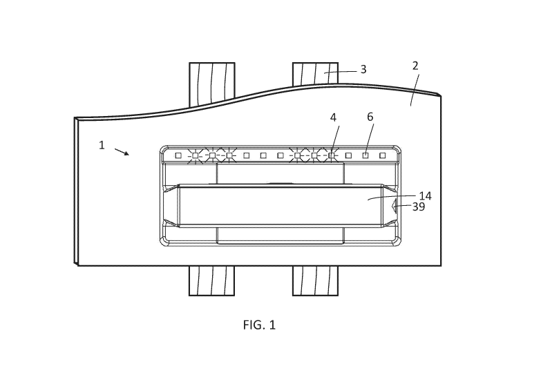
[0038] FIG. 1 illustrates an obscured feature detector 1, according to one
embodiment, placed on a piece of sheetrock 2 (or similar surface) and
detecting an
obscured feature 3. FIG. 2 is a perspective view of the obscured feature
detector 1 of
FIG. 1. FIG. 3 shows a sensor side of the obscured feature detector 1, which
includes a plurality of sensor plates 5 and a shortened common plate 33.
[0039] With reference to FIGS. 1-3, generally and collectively, the
obscured
feature detector 1 includes three or more sensor plates 5, a sensing circuit
(see FIG.
6
CA 03050083 2019-07-12
WO 2018/132129 PCT/US2017/040857
4), one or more indicators 6, one or more proximity indicators 39, and a
housing 19
to provide or otherwise accommodate a handle 14, an active shield plate 23,
and a
battery cover 28.
[0040] The
three or more sensor plates 5 each can take a sensor reading that
varies based on a proximity of the sensor plate 5 to one or more surrounding
objects
and on a material property of each of the one or more surrounding objects. The
three
or more sensor plates 5 may collectively create a sensing field. Each
individual
sensor plate 5 of the three or more sensor plates 5 may create a corresponding
primary sensing field zone that may be a geometric three-dimensional volume
within
the sensing field where the individual sensor plate 5 contributes more
strongly to the
sensing field than any other of the three or more sensor plates 5. The three
or more
sensor plates 5 may all create primary sensing field zones that are
geometrically
similar. The sensing circuit may couple to the three or more sensor plates 5
to
measure the sensor readings of the three or more sensor plates 5.
[0041] Each sensor plate 5 forms a first end of a corresponding electric
field. The
electric field is produced or received at the sensor plates 5. An area on the
common
plate 33 may form a second end of the corresponding electric field of each
sensor
plate 5. The common plate 33 has a length extending along one side of each of
the
sensor plates 5. The length of the common plate 33 is less than a collective
linear
dimension of the sensor plates 5. In some embodiments, the common plate 33 is
coupled to a non-changing voltage. In some embodiments the common plate 33 is
coupled to the circuit ground. In
some embodiments the common plate 33 is
coupled to an alternating signal.
[0042] In
some embodiments each sensor plate 5 may be part of a group 7 or
array of sensor plates 5. Each group 7 may include two or more sensor plates 5
and
may also include an active shield plate 23. The sensor plates 5 and active
shield
plate 23 may be on different planes. Nevertheless if they are driven
simultaneously,
in some embodiments, they may be part of the same group 7 of sensor plates 5.
Each sensor plate 5 has a geometry that is defined by its shape. Each sensor
plate 5
also has a perimeter. In some embodiments the perimeter may be composed of
multiple segments. In some embodiments each segment of the perimeter is either
an
internal border 10, or an external border 11. In some embodiments, if a sensor
plate
has a segment of the perimeter that is adjacent to the perimeter of the group
7,
then said segment comprises an external border 11. In some embodiments, if a
7
CA 03050083 2019-07-12
WO 2018/132129 PCT/US2017/040857
sensor plate 5 has a segment of the perimeter that is not adjacent to the
perimeter of
the group 7, then said segment comprises an internal border 10.
[0043] In some embodiments to sense the location of an obscured feature 3,
a
sensor plate 5 may be driven with a current source, and the obscured feature
detector 1 measures the time it takes for the sensor plate 5 to reach a
certain
threshold voltage, thereby achieving a sensor reading. In other embodiments a
charge-share mechanism is used to achieve a sensor reading. In other
embodiments
a radio frequency signal is placed on the sensor plates 5 to achieve a sensor
reading. In each of these embodiments a signal is driven on the sensor
plate(s) 5 to
be sensed.
[0044] In some embodiments, only a single sensor plate 5 may be driven at a
time. In these embodiments the single sensor plate 5 may be alone in creating
the
sensing field.
[0045] In some embodiments, a group 7 of sensor plates 5 may all be driven
with
the same signal simultaneously. In these embodiments the group 7 of sensor
plates
may create the sensing field. In some embodiments multiple sensor plates 5 may
be driven simultaneously each with the same signal, although possibly only a
single
sensor plate 5 may be sensed. Advantageously driving multiple sensor plates 5
simultaneously may create field lines that go deeper into an obscured surface
than
may be possible if only a single sensor plate 5 is driven. Deeper field lines
may make
it possible to sense more deeply. In some embodiments a group 7 of sensor
plates 5
and an active shield plate 23 may all be driven with the same signal
simultaneously,
which together would create the sensing field.
[0046] Each sensor plate 5 has a primary sensing field zone. In some
embodiments the primary sensing field zone is a geometric three-dimensional
volume of the sensing field and associated field lines where the individual
sensor
plate 5 is able to sense more strongly than the active shield plate 23 (if
present), or
any other sensor plate 5. In some embodiments it is desirable for each sensor
plate
5 to have similar primary sensing field zones. In some embodiments it is
desirable
for each sensor plate 5 to have primary sensing field zones that are
geometrically
similar and to have similar sensing fields within their respective primary
sensing field
zones.
[0047] FIG. 3 illustrates thirteen sensor plates 5 arranged linearly to
form a
sensor array 7. Each of the sensor plates 5 is rectangular. Each sensor plate
is
8
CA 03050083 2019-07-12
WO 2018/132129 PCT/US2017/040857
configured to take a sensor reading that varies based on the proximity of the
sensor
plate 5 to one or more surrounding objects and on a material property of each
of the
one or more surrounding objects.
[0048] In some embodiments, as shown in FIG. 3, the sensor array 7 may
comprise sensor plates 5 that each have a similar geometry. In some
embodiments
the distance between adjacent sensor plates 5 may be approximately 2.0 mm. As
shown, a shortened common plate 33 extends along the sensor array 7 along one
side of each of the sensor plates 5. The length of the shortened common plate
33 is
less than the collective linear dimension of the sensor array 7. In some
embodiments, the shortened common plate 33 may not extend along a side of one
or both of the end sensor plates.
[0049] In FIG. 3 a sensing field may be created collectively by the sensor
plates
5. In some embodiments an active shield plate 23 may contribute to the sensing
field. In the embodiment of FIG. 3 each of the sensor plates 5 may have
similar
primary sensing field zones. In this embodiment, the shortened common plate 33
causes each sensor plate 5 to have primary sensing zones that are
geometrically
similar as explained in more detail with reference to FIG. 12, 15, and 16.
Likewise,
each of the sensor plates 5 may also have similar sensing fields within their
respective primary sensing field zones. As a result, an obscured feature
detector 1
that is built with a configuration of FIG. 3 may offer improved performance.
When the
obscured feature detector 1 is moved from a thin surface to a thicker surface
the
sensor readings for each of the sensor plates 5 may have a similar increase in
value.
[0050] In some embodiments a sawtooth-shape border or perimeter may have
the same effective border as a straight-line border that does not have a
sawtooth. In
some embodiments a border with a very slight curve may have the same effective
border as a straight-line border that does not have a slight curve. In some
embodiments a sensor plate 5 with a slot in it has the same effective geometry
as an
otherwise equivalent sensor plate 5 without a slot. In some embodiments a
sensor
plate 5 with a small hole in it may have the same effective geometry as an
equivalent
sensor plate 5 without a hole. Many other geometries are possible that may be
effectively equivalent to other substantially equivalent geometries. Many
other
borders are possible that may effectively be equivalent to other substantially
equivalent borders. If a geometry or a border has a property that is
effectively
9
CA 03050083 2019-07-12
WO 2018/132129 PCT/US2017/040857
equivalent to another geometry or border, then the two may be considered to be
similar.
[0051] In some embodiments a group 7 of sensor plates 5 is configured such
that
each sensor plate 5 in the group 7 has the same geometry. In some embodiments
each of the sensor plates 5 in the group 7 is radially symmetrical.
[0052] The plurality of indicators 6 may be toggled between a deactivated
state
and an activated state to indicate a location of a region of relative high
sensor
reading. Activated indicators 4 can indicate the position of the obscured
feature 3.
Proximity indicators 39 can indicate that the obscured feature detector 1 may
be
near the obscured feature 3.
[0053] In FIGS. 1-3, the indicators 6 are positioned on a layer above the
sensor
plates 5. In some embodiments there may be an active shield plate 23 between
the
sensor plates 5 and the indicators 6 so that the indicators 6 do not interfere
with the
function of the sensor plates 5. In some embodiments it may be desirable to
position
the indicators 6 on a layer above the sensor plates 5.
[0054] In some embodiments, a layer of protective material is mounted to
the
bottom of the obscured feature detector housing, such that there is a layer of
protective material between the surface 2 and the obscured feature detector 1.
In
some embodiments, the protective material has the interior substantially
filled such
that it is substantially free from cavities. In some embodiments the
protective
material is unlike felt, Velcro, cloth, or other materials that have an
interior with
cavities. The layer of protective material may serve the purpose of protecting
the
bottom of the obscured feature detector 1 from damage due to knocks, bumps,
and
wear-and-tear. The protective material could be made from a solid piece of
material,
such as plastic or other solid non-conductive materials. A solid layer of
plastic may
provide a low friction surface that would allow the obscured feature detector
1 to
slide across the wall. Although some embodiments of the obscured feature
detector
1 do not require sliding to operate, a low friction surface may be useful to
some
users that may choose to move the obscured feature detector 1 from position to
position by sliding it.
[0055] The protective layer of plastic may be mounted with a pressure
sensitive
adhesive, glue, or other means. The layer of protective material may be a
complete
layer that covers the entire surface; it may be rectangular strips, round
pieces, or
other layers of plastic with other geometries.
CA 03050083 2019-07-12
WO 2018/132129 PCT/US2017/040857
[0056] A protective material that is substantially filled such that it is
substantially
free from cavities may build up less static charge than prior art solutions
and may
advantageously provide for more consistent sensor readings.
[0057] In some embodiments the protective material is UHMW-PE (Ultra-High
Molecular Weight Polyethylene). UHMW-PE has a low coefficient of friction.
UHMW-
PE also absorbs very little moisture which may provide increased immunity from
changes in humidity, and may provide enhanced immunity from changes in
humidity.
[0058] FIG. 4 is a diagram of a circuit of an obscured feature detector 1,
according to one embodiment. The circuit includes a multiplexer 18, a power
controller 20, a display circuit 25, a sensing circuit 27, and a controller
60.
[0059] The power controller 20 may include a power source 22 and an on-off
button 24. The power source 22 can comprise an energy source for powering the
indicators 6 and supplying power to a capacitance-to-digital converter 21, and
a
controller 60. In some embodiments, the power source 22 can comprise a DC
battery supply. The on-off switch 24 can be used to activate the controller 60
and
other components of the obscured feature detector 1. In some embodiments, the
on-
off switch 24 comprises a push-button mechanism that activates components of
the
obscured feature detector 1 for a selected time period. In some embodiments
the
push button activates the components such that the components remain activated
until the button is released. In some embodiments the on-off switch 24
comprises a
capacitive sensor that can sense the presence of a finger or thumb over the
button.
In some embodiments, the on-off switch 24 can comprise a toggle switch, or
other
types of buttons or switches.
[0060] The display circuit 25 may include one or more indicators 6 that are
electronically coupled to the controller 60.
[0061] The sensing circuit 27 may include a voltage regulator 26 and the
capacitance-to-digital converter 21. In some embodiments, as shown in FIG. 4,
the
sensing circuit 27 comprises a plurality of sensors, the voltage regulator 26,
and the
capacitance-to-digital converter 21. The voltage regulator 26 may be used to
condition the output of the power controller 20, as desired. In some
embodiments the
voltage regulator 26 is placed as near as possible to the capacitance-to-
digital
converter 21, which may provide a better power source 22 to the capacitance-to-
digital converter 21. The sensing circuit 27 can be electrically coupled to
the
controller 60. One or more sensor plate traces 35, or electrically conductive
paths on
11
CA 03050083 2019-07-12
WO 2018/132129 PCT/US2017/040857
the PCB, may connect the individual sensor plates 5 to the capacitance-to-
digital
converter 21. The connection of the sensor plates 5 to the capacitance-to-
digital
converter 21 may be made via the multiplexer 18. The multiplexer 18 can
individually
connect the sensor plates 5 to the capacitance-to-digital converter 21.
[0062] In some embodiments the multiplexer 18 may connect a single sensor
plate 5 to the sensing circuit 27. In some embodiments, the multiplexer 18 may
connect more than one adjacent sensor plate 5 to the sensing circuit 27. In
some
embodiments, the multiplexer 18 may connect more than one non-adjacent sensor
plate 5 to the sensing circuit 27. In some embodiments, the multiplexer 18 is
configured so that the sensing circuit 27 measures the capacitance of one
sensor
plate 5. In some embodiments, the multiplexer 18 is configured so that the
sensing
circuit 27 measures the aggregate capacitance of two or more sensor plates 5.
[0063] Each individual sensor plate 5 of a group 7 can be independently
connected to the capacitance-to-digital converter 21 via the multiplexer 18.
In some
embodiments, the group 7 itself is comprised of layers of copper on a PCB.
[0064] In some embodiments a two-layer PCB is configured as a sensor plate
board 40 (see FIG. 6). In some embodiments a first layer of the sensor plate
board
40 comprises the sensor plates 5, and a second layer of the sensor plate board
40
comprises a shield. In some embodiments, the shield is comprised of a layer of
copper that covers the entire surface of the second layer of the PCB. In some
embodiments the layer of copper is covered with a non-conductive layer of
soldermask. In some embodiments there are holes in the layer of soldermask. In
some embodiments, the holes in the layer of soldermask comprise solder pads
that
are suitable for making solder bonds.
[0065] In some embodiments a four-layer PCB is configured as an
interconnection board that has interconnections suitable for connecting
circuitry
components. In some embodiments the interconnection board is configured with
four
layers of interconnections that are suitable for interconnecting the sensing
circuit 27,
the controller 60, and the display circuit 25. In some embodiments one side of
the
PCB is configured for mounting components, and a second side of the PCB is
configured with solder pads.
[0066] In some embodiments the sensor plates 5 are arranged on a first PCB.
In
some embodiments the interconnection circuitry is arranged on a second PCB. In
some embodiments the first PCB is bonded to the second PCB.
12
CA 03050083 2019-07-12
WO 2018/132129 PCT/US2017/040857
[0067] In some embodiments there are solder pads on the sensor plate board
40
that are complementary with solder pads on an interconnection board. In some
embodiments the sensor plate board 40 and the interconnection board may be
stacked on top of one another and bonded to each other. In some embodiments
the
bonding agent that bonds the two PCBs together may be solder. In some
embodiments solder paste may be used to bond two PCBs together. In some
embodiments, they may be bonded together with solder and the process to bond
them together may be standard SMT (surface mount technology) processes. The
standard SMT process may include using a stencil to place solder paste in the
desired locations. The SMT process may include placing one PCB on top of
another.
In some embodiments pins may be used to ensure proper alignment of the two
PCBs. In some embodiments the final step of the SMT process may involve
running
the stacked PCBs through a reflow oven.
[0068] In some embodiments the sensor plates 5, shield, and circuitry are
placed
on a single PCB. In some embodiments a six-layer PCB is used. In some
embodiments the bottom layer, which is the sixth layer, of the PCB is
configured with
sensor plates 5. The fifth layer may be an active shield. The top four layers
may
connect the balance of the circuitry.
[0069] In some embodiments the sensor plates 5, shield, and circuitry are
placed
on a single PCB. In some embodiments a four-layer PCB is used. First and
second
layers of the PCB are configured with interconnection circuitry. In some
embodiments the bottom layer, which is the fourth layer, of the PCB is
configured
with sensor plates 5. The third layer may be an active shield.
[0070] The PCB can be made from a variety of suitable materials, such as,
for
example, FR-4, FR-406, or more advanced materials used in radio frequency
circuits, such as Rogers 4003C. Rogers 4003C, and other radio-frequency-class
PCB substrates, may offer improved performance across a broader temperature
and
humidity range.
[0071] As used herein, the term "module" can describe any given unit of
functionality that can perform in accordance with one or more embodiments of
the
present invention. For example, a module might by implemented using any form
of
hardware or software, or a combination thereof, such as, for example, one or
more
processors, controllers 60, ASICs, PLAs, logical components, software
routines, or
other mechanisms.
13
CA 03050083 2019-07-12
WO 2018/132129 PCT/US2017/040857
[0072] Different processes of reading a capacitance and converting it to a
digital
value, also known as a capacitance-to-digital conversion, are well-described
in the
prior art. The many different methods are not described here, and the reader
is
referred to the prior art for details about different capacitance-to-digital
converter
methods. Some embodiments use a sigma-delta capacitance-to-digital converter,
such as the one that is built into the Analog Devices AD7747 integrated
circuit. Some
embodiments use a charge-sharing method of capacitance-to-digital conversion.
[0073] In some embodiments the voltage regulator 26 may comprise the
ADP150-2.65 from Analog Devices, or the NCP702 from ON Semiconductor, which
provide very low noise. In some embodiments, the controller 60 may comprise
the
C8051 F317 from Silicon Laboratories, or any of many other microcontrollers.
[0074] Detecting obscured features 3 can require a high degree of accuracy,
and
may require more accuracy than a capacitance-to-digital converter 21 may be
able to
provide, if the native capacitance-to-digital converter sensor readings are
used
alone. Native sensor readings are the raw values read from the capacitance-to-
digital converter 21; they are the digital output of the capacitance-to-
digital converter
21.
[0075] Some embodiments perform native reads multiple times, and combine
the
results of the multiple native reads, to create a reading. Some embodiments
perform
native reads multiple times, and combine the results of the multiple native
reads,
using a different configuration for two or more of the native reads to create
a reading.
Some embodiments perform native reads multiple times, and sum or average the
results of the multiple native reads, to create a reading. In some embodiments
this
improves the signal-to-noise ratio. Each native read may involve reading one
sensor
plate 5. A native read could also involve reading a plurality of sensor plates
5, if
multiple sensor plates 5 are multiplexed to the capacitance-to-digital
converter 21. In
some embodiments multiple native reads are combined to create a reading.
[0076] Summing or averaging multiple native reads may improve the signal-to-
noise ratio, but may not reduce the effect of non-linearities in the
capacitance-to-
digital converter 21. The ideal capacitance-to-digital converter 21 is
perfectly linear,
which means that its native sensor readings increase in direct proportion to
an
increase in the capacitance being sensed. However, many capacitance-to-digital
converters 21 may not be completely linear, such that a change in the input
capacitance does not result in an exactly proportional increase in the native
reading.
14
CA 03050083 2019-07-12
WO 2018/132129 PCT/US2017/040857
These non-linearities may be small, but when a high degree of accuracy is
desired it
may be desirable to implement methods that reduce the effects of the non-
linearities.
[0077] In some embodiments, the ill effects of the non-linearities may be
mitigated by summing multiple native reads, using a slightly different
configuration
for each of the native reads. Some embodiments perform native reads using two
or
more different configurations.
[0078] For example, the bias current is one parameter that can be altered
to
create different configurations. The bias current could be set to normal, or
normal
+20%, normal +35%, or normal +50%. Different bias currents produce different
native sensor readings, even if all other factors remain constant. Since each
native
reading has a different value, presumably each native reading may be subject
to
different non-linearities. Presumably summing or averaging sensor readings
that are
subject to different non-linearities may cause the non-linearities to
partially cancel
each other out, instead of being summed, or multiplied.
[0079] In some embodiments there are two separate and independent
capacitance-to-digital converters 21. In some embodiments each of them may
have
different non-linearities. Using both of the capacitance-to-digital converters
21, using
a first converter for some of the reads and using the second converter for
some of
the reads, may mitigate the effect of any single non-linearity.
[0080] Some embodiments perform native reads on each of the sensor plates 5
using each of twelve different configurations.
[0081] After completing the sensor readings, in some embodiments, two
different
calibration algorithms may be performed: first an individual-plate calibration
that
adjusts for individual sensor plate 5 variations, and second a surface
material
calibration that adjusts the sensor readings so that they are tuned to the
surface
density/thickness. Other embodiments may only use one of the two calibration
algorithms. Some embodiments may use other calibration algorithms. In some
embodiments the calibration algorithms are performed by a calibration module.
[0082] In some embodiments, individual plate calibration is employed first.
With
individual plate calibration, each sensor plate 5 may have its own individual
calibration value. In some embodiments, after the sensor readings are taken,
an
individual plate calibration value is added to, or subtracted from, each of
the sensor
readings. Other embodiments may use multiplication, division, or other
mathematical
functions to perform the individual plate calibration. In some embodiments,
the
CA 03050083 2019-07-12
WO 2018/132129 PCT/US2017/040857
individual plate calibration value is stored in non-volatile memory.
Individual plate
calibration compensates for individual sensor plate 5 irregularities, and is
used to
compensate for these irregularities. In some embodiments it is presumed that
after
performing individual plate calibration that the sensor readings will
presumably have
the same calibrated values, if the sensor plate sensor readings are taken
while the
obscured feature detector 1 is on the surface 2 that is similar to the surface
2 the
obscured feature detector 1 was calibrated on. For example, if sensor readings
are
performed on 1/2" sheetrock 2, without any obscured features 3 present, and
the
individual calibration values were created for 1/2" sheetrock 2, then after
performing
individual plate calibration, it is presumed that all the sensor readings
would be
corrected to a common value. If sensor readings are performed on a thicker
material
(such as 5/8" sheetrock 2), a thinner material (such as 3/8" sheetrock 2), or
a
different material (such as 3/4" plywood) then there may be some error in the
values.
Surface material calibration may help correct this error.
[0083] In some embodiments surface material calibration may be used.
[0084] In some embodiments, after calibrating the sensor plate sensor
readings
the obscured feature detector 1 decides if an obscured feature 3 is present.
In some
embodiments the lowest sensor plate reading is subtracted from the highest
sensor
plate reading. If the difference is greater than a threshold value then a
determination
is made that an obscured feature 3 is present.
[0085] If it is determined that no obscured features 3 are present, then
all of the
indicators 6 may be deactivated. If an obscured feature 3 is present then the
obscured feature detector 1 begins the process of determining the position(s)
and
width(s) of the obscured feature(s) 3.
[0086] In some embodiments pattern matching may be employed to determine
which LEDs to activate. In some embodiments a pattern matching module is used
to
determine the locations of obscured features 3. The pattern matching module
compares the calibrated and scaled sensor readings from the sensor plates 5 to
several predetermined patterns. The pattern matching module determines which
predetermined pattern best matches the sensor readings. Then the set of
indicators
6 that corresponds to the best matching pattern is activated. Additional
details about
pattern matching are discussed in the prior art, such as in U.S. Patent No.
8,884,633. Those details will not be repeated here; instead the reader is
encouraged
to refer to them directly.
16
CA 03050083 2019-07-12
WO 2018/132129 PCT/US2017/040857
[0087] In some embodiments the obscured feature detector 1 comprises a
single
capacitance-to-digital converter 21. In some embodiments the sensor plates 5
may
be individually connected to the capacitance-to-digital converter 21. In some
embodiments the sensor plates 5 may be individually connected to the
capacitance-
to-digital converter 21 via the multiplexer 18. In some embodiments more than
one
sensor plate 5 may be connected to the capacitance-to-digital converter 21 at
a time.
In some embodiments multiple adjacent sensor plates 5 may be electrically
connected to the capacitance-to-digital converter 21. In some embodiments
multiple
non-adjacent sensor plates 5 may be connected to the capacitance-to-digital
converter 21. The use of a multiplexer 18 to connect sensor plates 5 to a
single
capacitance-to-digital converter 21 may improve sensor plate 5 to sensor plate
5
consistency of the sensor readings, because the sensor readings from each of
the
sensor plates 5 may be equally affected by variations to the capacitance-to-
digital
converter 21. Factors that may affect the sensor readings from the capacitance-
to-
digital converter 21 may include, but are not limited to, process variations,
temperature variations, voltage variations, electrical noise, aging, and
others.
[0088] In some embodiments, the sensor plate traces 35 are routed such that
each of the sensor plate traces 35 has substantially equal capacitance,
resistance,
and inductance. In some embodiments it is desirable for each of the sensor
plate
traces 35 to have the same electrical properties, so that each of the sensor
plates 5
will respond equivalently to the same detected object(s).
[0089] In some embodiments each of the sensor plate traces 35 from the
capacitance-to-digital converter 21 to each of the sensor plates 5 has
substantially
the same length. In some embodiments two or more of the sensor plate traces 35
from the capacitance-to-digital converter 21 to the sensor plates 5 have
substantially
the same length. In some embodiments sensor plate traces 35 with substantially
the
same length may have more equivalent capacitances, inductances, and
resistances.
Equal length sensor plate traces 35 may offer enhanced performance because
they
may improve the uniformity of the sensor readings, such that the sensor plates
5
respond more equivalently to the same detected objects, and may provide more
immunity from environmental conditions, such as temperature and humidity.
[0090] In some embodiments each of the sensor plate traces 35, which
comprises electrically conductive paths, has substantially the same width. In
some
embodiments, both the width and the length of each of the sensor plate traces
35 are
17
CA 03050083 2019-07-12
WO 2018/132129 PCT/US2017/040857
substantially equivalent. In some embodiments the sensor plate traces 35 will
have
more than one segment. For example, a first segment of the traces may route
the
sensor plate traces 35 from a capacitance-to-digital converter 21 to a via.
The via
may take the sensor plate trace 35 to a different layer of the PCB, where
there may
be a second segment of the sensor plate trace 35. In some embodiments all of
the
sensor plate traces 35 will have the same length and width, in each segment,
as the
other traces in that segment. In some embodiments two or more of the sensor
plate
traces 35 will have the same width throughout a first segment. In some
embodiments
two or more of the sensor plate traces 35 will have the same width throughout
a
second segment. In some embodiments two or more of the sensor plate traces 35
will have the same length throughout a first segment. In some embodiments two
or
more of the sensor plate traces 35 will have the same length throughout a
second
segment.
[0091] In some embodiments the sensor plate traces 35 comprise multiple
segments. In some embodiments a segment of a sensor plate trace 35 may be the
wire bonds that are within the package of an integrated circuit that route the
signals
from the piece of silicon to the pins of the integrated circuit package. In
some
embodiments a segment of a sensor plate trace 35 may comprise a layer of
copper
on a first layer of a PCB. In some embodiments a segment of a sensor plate
trace 35
may comprise a layer of copper on a second layer of a PCB.
[0092] In some embodiments the capacitance-to-digital converter 21 will
read the
sum of the capacitance on the sensor plates 5 and the capacitance on the
sensor
plate traces 35. In some embodiments, only detecting the sensor readings on
the
sensor plates 5, and not detecting the sensor plate traces 35, may be
preferable.
However, because the sensor plates 5 and sensor plate traces 35 are
electrically
coupled, a means of ensuring stable and uniform capacitance on the sensor
plate
traces 35 may be desired. For example, it may be desirable to configure the
sensor
plate traces 35 so that their capacitance is uniform and stable. Consequently,
it may
be preferred for the sensor plate traces 35 to be configured so that the
sensor plate
traces 35 do not change. In some embodiments it may be preferred that the
sensor
plate traces 35 do not change relative to each other, such that any change in
the
capacitance on one sensor plate trace 35 is reflected in each of the sensor
plate
traces 35.
18
CA 03050083 2019-07-12
WO 2018/132129 PCT/US2017/040857
[0093] In some embodiments it may be advantageous to shield the sensor
plate
traces 35. Sensor plate trace shielding may protect the sensor plate traces 35
from
external electromagnetic fields. In some embodiments shielding the sensor
plate
traces 35 may also advantageously provide a more consistent environment for
the
sensor plate traces 35 by helping to ensure that each of the sensor plate
traces 35
has an environment that is similar to each of the other sensor plate traces
35.
[0094] In some embodiments each of the sensor plate traces 35 from the
capacitance-to-digital converter 21 to each of the sensor plates 5 has
substantially
the same surroundings. In some embodiments the sensor plate traces 35 are
routed
sufficiently far apart so that capacitive and inductive coupling between the
sensor
plate traces 35 is minimized, and may improve consistency because each of the
sensor plate traces 35 may have surroundings that are more similar to the
other
sensor plate traces 35. In some embodiments each of the sensor plate traces 35
is
shielded on one or both sides with an active shield trace.
[0095] In some embodiments a user may be electrically coupled to the
sensing
circuit 27. In some embodiments the quality of the sensor readings is
increased
when an electrically conductive point of the sensing circuit 27 is coupled to
the user.
Electrically coupling the user to the sensing circuit 27 may provide a
stationary
voltage level for the sensing circuit 27 and may result in higher quality
sensor
readings that have higher sensitivity. For example, a prior art obscured
feature
detector that drives the sensor plates 5 with a 3.0V may in reality only drive
the
sensor plates 5 with a 3.0V signal relative to ground. However, if the ground
is
floating, then driving the sensor plates 5 with 3.0V could result in a 1.5V
signal on
the sensor plates 5, and a -1.5V signal on the ground. In some embodiments the
quality of the sensor readings is not increased when an electrically
conductive point
of the sensing circuit 27 is coupled to the user.
[0096] In some embodiments electrically coupling the user to the sensing
circuit
27 may result in higher absolute voltage swings on the sensor plates 5, which
may
be due in part to the sensing circuit 27 being held at a stable level. In some
embodiments electrically coupling the user to the sensing circuit 27 may also
result
in sensor readings that are more consistent.
[0097] In some embodiments the user is electrically coupled to the ground
of the
sensing circuit 27, as shown in FIG. 4. In some embodiments the user is
electrically
coupled to the voltage source of the sensing circuit 27. In some embodiments
the
19
CA 03050083 2019-07-12
WO 2018/132129 PCT/US2017/040857
user is electrically coupled to a different electrically conductive point of
sensing
circuit 27.
[0098] In some embodiments the hand of the user may be electrically coupled
to
the sensing circuit 27 by making direct contact with the sensing circuit 27.
In some
embodiments an electrically conductive material, such as a wire, may
electrically
couple the hand of the user to the sensing circuit 27. In some embodiments the
button, which the user would need to touch to activate the obscured feature
detector
1, may comprise an electrically conductive material which may be electrically
coupled to the sensing circuit 27. In some embodiments the button may comprise
aluminum or another electrically conductive material such as tin-plated steel.
In
some embodiments an aluminum button may be anodized, which may provide
pleasing cosmetics.
[0099] In some embodiments the housing 19 (see FIG. 2) of the obscured
feature
detector 1 may comprise an electrically conductive material, such as an
electrically
conductive plastic. In some embodiments only a portion of the housing 19 may
comprise electrically conductive plastic. The electrically conductive housing,
or a
portion of the electrically conductive housing may be coupled to an
electrically
conductive point in the sensing circuit 27, thereby coupling the user to the
sensing
circuit 27.
[00100] In some embodiments mixing carbon black with the plastic resin may
provide electrically conductive properties. Many thermoplastics, including
polypropylene and polyethylene, become electrically conductive when a carbon
black is mixed into the plastic resin. In some embodiments the conductivity
increases
as the concentration of carbon black is increased, advantageously making it
possible
to control the conductivity of the plastic. In some embodiments a plastic with
a
conductivity that is less than about 25,000 ohms-cm provides sufficiently high
conductivity to effectively couple the user to the sensing circuit 27. In some
embodiments a higher degree of conductivity may be desired. In some
embodiments
a lower degree of conductivity may be desired. In some embodiments it is
advantageous for the user to be coupled to the sensing circuit by a path with
less
than about fifty mega-ohms.
[0101] In some prior art obscured feature detectors, a change in the
position of
the hand of the user can cause a change in the sensor readings. This may occur
in
some prior art obscured feature detectors because the hand may form a portion
of
CA 03050083 2019-07-12
WO 2018/132129 PCT/US2017/040857
the path between the sensor plates 5 and ground. As a result, a change in hand
position can cause a change in the sensor readings of the sensor plates 5.
Disadvantageously, this may reduce the accuracy of the sensor readings.
[0102] If it were possible for the size and position of the hand of the
user to be
constant, it may be possible to do a calibration adjustment to mathematically
remove
the effect of the hand of the user from the raw sensor readings. However, in
practice
this may not be feasible. In practice the size, shape, and position of hands
of
different users may vary too much to make a calibration adjustment practically
possible.
[0103] To improve performance in light of the aforementioned issues, in
some
embodiments a conductive hand guard may be positioned between the hand of the
user and the sensor plates 5. In some embodiments the hand guard may be
grounded to the sensing circuit 27, as illustrated in FIG. 4.
[0104] FIG. 5 is a diagram of the controller 60, according to one
embodiment. The
controller 60 includes a processor 61, a clock 62, random access memory (RAM)
64,
a non-volatile memory 65, and/or another computer-readable medium. The non-
volatile memory 65 may include a program 66 (e.g., in the form of program code
or
computer-executable instructions for performing operations) and calibration
tables
68. In operation, the controller 60 may receive the program 66 and may
synchronize
the functions of the capacitance-to-digital converter 21 and the display
circuit 25 (see
FIG. 4). The non-volatile memory 65 receives and stores the program 66 as well
as
look-up tables (LUT) and calibration tables 68. The program 66 can include a
number of suitable algorithms, such as, for example, an initialization
algorithm, a
calibration algorithm, a pattern-matching algorithm, a multiplexing algorithm,
a
display management algorithm, an active sensor activation algorithm, and a non-
active sensor management algorithm.
[0105] FIG. 6 is a cross-sectional view of an obscured feature detector,
according
to one embodiment, including a housing, with light pipes and a button, and a
printed
circuit board. In some embodiments, as shown in FIG. 6, a housing 19 comprises
an
upper housing, an on-off switch 24, a handle 14, a plurality of light pipes 8,
and a
power supply compartment. In some embodiments a conforming core may be
configured to flexibly couple the housing 19 to a sensor plate board 40. In
some
embodiments the sensor plate board 40 is a multi-layered printed circuit board
with a
top layer 44, a second layer 43, a third layer 42, and a bottom layer 41. In
some
21
CA 03050083 2019-07-12
WO 2018/132129 PCT/US2017/040857
embodiments the sensor plate board 40 is a multi-layered printed circuit board
that
couples a capacitance-to-digital converter 21, a display circuit 25, and a
controller
60, as described above with reference to FIG. 4. In some embodiments, the
housing
19 comprises plastic. In some embodiments, the housing 19 comprises ABS
plastic.
In some embodiments a conductive hand guard 56 shields the user's hand from
the
sensor plate board 40. In some embodiments the hand guard 56 is connected to
the
ground of a sensing circuit.
[0106] In some embodiments, the handle 14 comprises a gripping surface. In
some embodiments a portion of the gripping surface comprises an elastomer that
makes the handle 14 easier to grip. The handle 14 is preferably positioned so
that
the user's hand does not obscure a view of the indicators 6 when grasping the
handle 14. In some embodiments, the power supply compartment comprises a
cavity
for holding a suitable power supply, such as batteries, and a battery cover
for
accessing the compartment.
[0107] In some embodiments the hand guard 56 may be configured so that
there
are no significant straight-line paths between the sensor plates and the
user's hand.
In some embodiments the housing 19 may be composed of an electrically
conductive material which may comprise the hand guard 56. In some embodiments
the conductive layer of material of the hand guard 56 may be a layer of
conductive
plastic. In some embodiments the conductive layer of material of the hand
guard 56
may be a layer of a different conductive material, such as a conductive paint.
In
some embodiments the conductive layer of material of the hand guard 56 may be
a
sheet of metal that is hidden within the housing 19. In some embodiments the
hand
guard 56 may comprise tin-plated steel, which may provide for quick, easy and
reliable solder joints. In some embodiments an entire layer of a PCB may
comprise
the hand guard 56. In some embodiments only a portion of a layer of a PCB may
comprise the hand guard 56, because in some embodiments it may not be
necessary to for the hand guard 56 to comprise an entire layer. For example a
ring
around the outside of a PCB may be an effective hand guard 56.
[0108] In some embodiments this hand guard 56 is configured to minimize an
effect of a size and position of the hand. In some embodiments the hand guard
56 is
positioned so that it is near the hand because in some embodiments it may be
most
effective when it is nearest to the hand. In some embodiments the hand guard
56
may be electrically coupled to the ground of a sensing circuit 27 (see FIG.
4). In
22
CA 03050083 2019-07-12
WO 2018/132129 PCT/US2017/040857
some embodiments the hand guard 56 may be coupled to the voltage of the
sensing
circuit 27. In some embodiments a different electrically conductive point of
the
sensing circuit 27 may be electrically coupled to the hand guard 56. In some
embodiments an electrical wire comprises the electrical path between the hand
guard 56 and the sensing circuit 27.
[0109] In
prior art obscured feature detectors a set of identical sensor plates 105
are typically arranged in a linear fashion, such as is shown in FIGS. 7, 8, 9,
and 10.
FIG. 7 is a prior art obscured feature detector 101 placed on a comparatively
thinner
surface 12. FIG. 8 is the prior art obscured feature detector 101 placed on a
comparatively thicker surface 13. FIG. 9 shows a side view of the prior art
obscured
feature detector 101, illustrating primary sensing field zones 15, 16, 17 for
several
sensor plates 105, including sensor plates A, B, C, D, E. FIG. 10 shows an
elevation
view of a bottom surface of the prior art obscured feature detector 101,
illustrating
the primary sensing field zones 15, 16, 17 for sensor plates A, B, C, D, E.
[0110]
Referring generally and collectively to FIGS. 7-14, each of the sensor
plates 105 performs a sensor reading of the surface 2. The sensor readings are
then
compared. The sensor plates 105 that have the highest sensor readings are
interpreted to be the locations of obscured features. However, as shown in
FIG. 7
and FIG. 8, the sensor plates 105 that are near the ends of the group may not
respond to obscured features in the same manner as the sensor plates 105 that
are
near the center. This issue may be particularly evident when the prior art
obscured
feature detector 101 is moved from the thinner, or less dense, surface 12, to
an
thicker, or more dense, surface 13.
[0111]
FIG. 7 shows representative sensor readings of the prior art obscured
feature detector 101 that is placed on the relatively thinner surface 12. The
relatively
thinner surface 12 could be 0.375-inch-thick sheetrock. FIG. 8 shows
representative
sensor readings of the prior art obscured feature detector 101 that is placed
on a
relatively thicker surface 13. The relatively thicker surface 13 could be
0.625-inch-
thick sheetrock.
[0112] In
FIG. 7, the prior art obscured feature detector 101 is placed on the
relatively thinner surface 12. Each of the sensor plates 105 may have a
calibration
adjustment so that each has a calibrated reading of, for example, 100. If this
same
prior art obscured feature detector 101 is then moved to another surface 13
that is
thicker, or to a surface that has a higher dielectric constant, the sensor
readings
23
CA 03050083 2019-07-12
WO 2018/132129 PCT/US2017/040857
would change. An image of the same prior art obscured feature detector 101 on
the
thicker surface 13 is shown in FIG. 8. Ideally each of the sensor plates 105
on the
thicker surface 13 would have similar sensor readings to each other, because
they
are all on the same thicker surface 13, with no obscured features present.
However,
it may be observed that the sensor readings of the sensor plates 105 near the
ends
may see a larger reading increase than the sensor plates 105 near the center.
In
FIG. 8, it may be seen that the sensor plates 105 near the center have sensor
readings of 200, but the sensor plates 105 at the ends have sensor readings of
250.
[0113] In the prior art obscured feature detector 101 of FIG. 8, and other
prior art
obscured feature detectors, the sensor plates 105 that are at the ends are
alone in
creating electric fields 9 that extend beyond the edges of the group of sensor
plates
105. As a result, the sensor plates 105 near the end may respond with a
disproportionately higher reading when placed on a thicker surface 13.
Disadvantageously, the controller 60 may have difficulty determining if the
elevated
sensor readings are due to the presence of an obscured feature, or due to the
prior
art obscured feature detector 101 being placed on the thicker surface 13. The
disclosed embodiments may address these and other challenges.
[0114] FIG. 9 illustrates the field lines for the prior art obscured
feature detector
101 of FIGS. 7 and 8. FIG. 9 shows a group of sensor plates 105 and also shows
a
two-dimensional representation of the field lines for each of the sensor
plates 105.
The field lines are shown for illustrative purposes and are a representation
of the
actual sensing field. The field lines drawn are equipotential electric field
lines.
However, this drawing does not limit the scope of the disclosure to this type
of field
alone. Vector electric field lines or magnetic field lines could have been
illustrated in
the drawing and are within the scope of the disclosure. The sensing field may
be an
electric field, or it may be a magnetic field, or it may be an electromagnetic
field,
which is a combination of an electric field and a magnetic field.
[0115] In FIG. 9 there are thirteen sensor plates 105. All of the sensor
plates 105
may be driven with the same signal simultaneously, while one sensor plate 105
at a
time is sensed. Because the sensor plates 105 are driven simultaneously, with
the
same signal, the sensing field is defined by the field created by the group of
sensor
plates 105, as illustrated in FIG. 9. An active shield plane is not
illustrated in the
figure, but an active shield may contribute to the sensing field in some
embodiments.
Five of the sensor plates 105 are labeled A, B, C, D, E. The field lines
emanating
24
CA 03050083 2019-07-12
WO 2018/132129 PCT/US2017/040857
from sensor plate E are primarily parallel to sensor plate E. However, the
field lines
emanating from sensor plate A are not very parallel to sensor plate A. Because
the
field lines do not have similar direction and strength at each point within
the primary
sensing field zone the sensor plates A and E do not have similar sensing
fields
within their primary sensing field zones.
[0116] In contrast, sensor plate D and sensor plate E have similar primary
sensing field zones because the volume of the sensing field where they are
able to
sense effectively and the sensing field within that primary sensing field zone
are
similar. The sensing fields within a primary sensing field zone are similar if
the
direction of the sensing field and strength of the sensing field are similar
at each
point within the primary sensing field zone.
[0117] FIG. 10 illustrates the same concept from a different angle or
perspective.
In FIG. 10 the five sensor plates 105 are again labeled A, B, C, D, E. The
approximate primary sensing field zones for each of the sensor plates 105 are
highlighted. On the two-dimensional drawing of FIG. 10, the primary sensing
field
zone 15 for sensor plate A is indicated by the drawing of the sensing field
lines for
sensor plate A. On the two-dimensional drawing of FIG. 10, the primary sensing
field
zone 16 for sensor plate B is indicated by the drawing of sensing field lines
for
sensor plate B. On the two-dimensional drawing of FIG. 10, the primary sensing
field
zone 17 for sensor plate C is indicated by the drawing of sensing field lines
for
sensor plate C.
[0118] FIGS. 9 and 10 illustrate the primary sensing field zone with a two-
dimensional drawing. However, in reality a three-dimensional primary sensing
field
zone may exist. There may be a three-dimensional zone for each sensor plate
105
that comprises the primary sensing field zone for each given sensor plate 105.
In
contrast to the prior art embodiment of FIGS. 9 and 10, in some embodiments of
the
present disclosure the sensor plates 105 may have an equivalent primary
sensing
field zone. Each sensor plate 105 in a group that has an equivalent primary
sensing
field zone may have an equivalent response to change in surfaces. This
disclosure
illustrates some configurations wherein each sensor plate 105 in a group may
have
an equivalent primary sensing field zone. In some embodiments each sensor
plate
105 with a similar primary sensing field zone may have a similar change in
sensor
readings in response to a change in the detected surface.
CA 03050083 2019-07-12
WO 2018/132129 PCT/US2017/040857
[0119] FIG. 11 is a flow diagram of a method 200 of detecting an obscured
feature
behind a surface, according to one embodiment. A first operation, as
illustrated in the
flow diagram in FIG. 11, may be to initialize a detector 202, which may
involve
running an initialization algorithm. The detector may be according to one of
the
embodiments described herein. After initialization, the sensor plates may be
read
204. In some embodiments each of the sensor plates may be read multiple times,
each time using a different configuration. The different configurations may
comprise
different drive currents, different voltage levels, different sensing
thresholds, or other
different configuration parameters. Each of these readings of the sensor
plates may
be referred to as native readings. In some embodiments multiple native
readings
may be added together to comprise a reading. In some embodiments there may be
a
separate reading for each sensor plate.
[0120] In some embodiments, each of these readings has a calibration 206
adjustment performed that is achieved by adding a predetermined calibration
value
to each reading. In some embodiments, after calibration, the readings for each
of the
sensor plates would be the same if the detector were to be placed on a uniform
surface.
[0121] In some embodiments, the largest sensor plate reading is compared
208
to the lowest sensor plate reading. The difference is then compared 208 to a
threshold value. In some embodiments, if the difference is less than a
predetermined
threshold value, then all of the indicators may be turned off 210, to indicate
that no
stud is present. If the difference is larger than a predetermined threshold
value, then
a determination may be made as to which indicators to activate. In certain
embodiments, the readings may be scaled 212 to a predetermined range, which
may
involve setting the lowest value to a number such as 0, and scaling the
largest
reading to a value such as 100. Then all of the intermediate values would be
scaled
proportionately. The scaled readings may then be compared 214 to predetermined
patterns which are scaled in a similar fashion.
[0122] In some embodiments there may be a set of predetermined patterns.
The
set of predetermined patterns may correspond to different combinations of
hidden
features that the detector may encounter. For example, the set of
predetermined
patterns may correspond to different positions for a single stud. In some
embodiments, the set of predetermined patterns may include positional
combinations
of two studs. A pattern matching algorithm may be employed to determine which
26
CA 03050083 2019-07-12
WO 2018/132129 PCT/US2017/040857
predetermined pattern best matches the reading pattern. The detector may then
activate 216 the indicators that correspond to the best matching predetermined
pattern.
[0123] In
other embodiments, after calibrating the sensor plate readings, a
determination is made if an obscured feature is present. The lowest sensor
plate
reading may be subtracted from the highest sensor plate reading. If the
difference is
greater than a threshold value, then a determination is made that an obscured
feature is present. If it is determined that no obscured features are present,
then all
of the indicators may be deactivated. If an obscured feature is present then a
process may begin to determine position(s) and/or width(s) of the obscured
feature(s). In some embodiments, all of the current sensor plate readings may
be
scaled such that the lowest reading is scaled to a predetermined value (such
as 0)
and the maximum reading is scaled to a second predetermined value (such as
100).
All intermediate values may be scaled proportionately. Scaled readings may be
easier to compare to a set of predetermined patterns.
[0124]
FIG. 12 is a prior art obscured feature detector 1200 configuration having
a typical plate configuration. As shown, the obscured feature detector 1200
may
comprise three or more sensor plates 5, a common plate 1202, and an active
shield
plate 23.
[0125] The
sensor plates 5, in the embodiment shown, are arranged linearly to
form a sensor array 7. As shown, the sensor plates 5 may have the same
geometry
and be evenly spaced. Each sensor plate 5 has an internal border extending
along at
least a portion of an internal border of one or more other sensor plates, and
an
external border disposed at an outer perimeter of the sensor array 7. The
linear
sensor array includes two end sensor plates 1210, 1212 and at least one non-
end
sensor plate 1214.
[0126]
Each sensor plate 5 is configured to take a sensor reading that varies
based on a proximity of the sensor plate to one or more surrounding objects
and on
a material property of each of the one or more surrounding objects. To
facilitate the
sensor reading, an area of each sensor plate 5 may form a first end of a
corresponding electric field.
[0127] The common plate 1202 may form a second end of the corresponding
electric field of each sensor plate 1202. The common plate 1202 has a length
1220
extending along a length 1222 of the sensor array, such that the common plate
1202
27
CA 03050083 2019-07-12
WO 2018/132129 PCT/US2017/040857
extends along one external border of each of the sensor plates 5. As shown,
the
common plate extends beyond an entire linear dimension of the sensor array 7.
Common plates of presently available plate configurations are at least 17
millimeters
longer than the sensor array, whether due to housing size or shape, shielding
configurations, or other reasons. The electric fields of the end sensor plates
formed
with such longer common plates are non-uniform in comparison to the electric
fields
formed by non-end sensor plates with such longer common plates.
[0128] FIG. 13 is an obscured feature detector 1300 having an improved
plate
configuration with a shortened common plate 1302. As shown, the obscured
feature
detector 1300 may comprise three or more sensor plates 5, a shortened common
plate 1302, and an active shield plate 23.
[0129] The sensor plates 5 in the embodiment shown are arranged linearly to
form a sensor array 7. As shown, the sensor plates 5 may have the same
geometry
and be evenly spaced. In other embodiments, the sensor plates 5 may vary in
size
and/or shape, and may be spaced differently based on the position of the
sensor
plate 5 in the sensor array 7. Each sensor plate 5 has an internal border
extending
along at least a portion of an internal border of one or more other sensor
plates, and
an external border disposed at an outer perimeter of the sensor array. The
linear
sensor array 7 includes two end sensor plates 1310, 1312 and at least one non-
end
sensor plate 1314.
[0130] Each sensor plate 5 is configured to take a sensor reading that
varies
based on a proximity of the sensor plate 5 to one or more surrounding objects
and
on a material property of each of the one or more surrounding objects. To
facilitate
the sensor reading, an area of each sensor plate 5 may form a first end of a
corresponding electric field.
[0131] The shortened common plate 1302 may form a second end of the
corresponding electric field of each sensor plate. The shortened common plate
1302
has a length 1320 extending along a length 1322 of the sensor array 7 such
that the
shortened common plate 1302 extends along the sensor array 7 and at least
partially
along one external border of each of the three or more sensor plates 5. In
some
embodiments, the shortened common plate may not extend along one or both of
the
end sensor plates. The length 1320 of the shortened common plate 1302 is less
than
the collective linear dimension of the sensor array 7 along which the
shortened
common plate 1302 extends. In the embodiment shown, the shortened common
28
CA 03050083 2019-07-12
WO 2018/132129 PCT/US2017/040857
plate 1302 is centered along the sensor array 7. In some embodiments, the
shortened common plate may be off-centered.
[0132] The active shield plate 23 separates the sensor plates 5 and the
shortened
common plate 1302. In the embodiment shown, the active shield plate 23
surrounds
the shortened common plate 1302 along three sides. In other embodiments the
active shield plate 23 may only run along the length 1320 of the shortened
common
plate 1302. However, having the active shield plate 23 surround the common
plate
may decrease the complexity of manufacturing.
[0133] In some embodiments, one sensor plate 5 may be sensed at a time. In
some embodiments when one sensor plate 5 is sensed, all of the sensor plates
5,
including the active shield plate 23, are driven with the same signal as the
sensed
sensor plate 5. The sensor array 7, plus the active shield plate 23, when
driven
together may push the field lines of the corresponding electric field deeper
into the
sensed surface than may be possible if just a single sensor plate 5 was
driven. In
some embodiments this allows field lines from a single sensor plate 5 to
penetrate
more deeply, and allows a single sensor plate 5 to sense more deeply, than may
be
possible if a single sensor plate 5 were driven alone.
[0134] FIG. 14 illustrates the electric fields created by the prior art
plate
configuration 1200 of FIG. 12. Each sensor plate 5 is configured to provide a
primary
coupling area 1402, 1412 to form a first end of a corresponding electric field
1406,
1408. Further, the common plate 1202 is configured to provide a corresponding
primary coupling area 1404, 1414 to correspond to a sensor plate 5 and form a
second end of the corresponding electric field 1406, 1408 of that sensor plate
5.
[0135] A primary coupling area 1402, 1412 is the area of a sensor plate 5
where
an electric field 1406, 1408 primarily couples. In the illustrated prior art,
a primary
coupling area 1402 of an end sensor plate 1210 is on a line 1420 with a
corresponding primary coupling area 1404 of the common plate 1202. Similarly,
a
primary coupling area 1404 of a non-end sensor plate 1214 is on a line 1422
with a
corresponding primary coupling area 1414 of the common plate 1202. As shown,
the
line 1420 of the primary coupling area 1402 of the end sensor plate 1210 to
the
corresponding primary coupling area 1404 of the common plate 1202 is
approximately parallel with the line 1422 of the primary coupling area 1404 of
the
non-end sensor plate 1214 to the corresponding primary coupling area 1414 of
the
common plate 1202.
29
CA 03050083 2019-07-12
WO 2018/132129 PCT/US2017/040857
[0136] As
shown, the electric field 1406 formed from the end sensor plate 1210 in
this configuration has a different geometry than the electric field 1408
formed from
the non-end sensor plate 1214. The electric fields generated by surrounding
sensing
plates 5 affect each other sensing plate 5. The non-uniform electric field
1406 is a
result of the end-sensor plate 1210 not having sensor plates 5 along both
sides. The
non-uniformity of the electric field 1406 may result in an inaccurate
detection or a
missed detection of obscured features. For
example, the electric field 1406
generated by the end sensor plate 1210 may penetrate more broadly into a
surface
than the electric filed 1408 generated by the non-end sensor plate 1214.
Because of
the different sensing areas, the end sensor plate 1210 may falsely identify an
obscured feature.
[0137]
FIG. 15 illustrates the electric fields 1506, 1508 created between an end
sensor plate 1310 and a non-end sensor plate 1314 in the plate configuration
of the
obscured feature detector 1300 of FIG. 13. Primary coupling areas (e.g., 1502,
1512) may couple the sensor plates 5 to the common plate 1302. Each of the
sensor
plates 5 is configured to provide a primary coupling area (e.g., 1502, 1512)
to form a
first end of a corresponding electric field. The common plate 1302 is
configured to
provide corresponding primary coupling areas (e.g., 1504, 1514) that each
correspond to a sensor plate 5 and forms a second end of the corresponding
electric
field of that sensor plate 5.
[0138] For
example, as shown, the end sensor plate 1310 is configured to provide
primary coupling area 1502 and the non-end sensor plate 1314 is configured to
provide primary coupling area 1512. The common plate 1302 is configured to
provide a corresponding primary coupling area 1504 that corresponds to the
primary
coupling area 1502 of the end sensor plate 1310 and a corresponding primary
coupling area 1514 that corresponds to the primary coupling area 1512 of the
non-
end sensor plate 1314.
[0139] As
illustrated, the electric fields 1506, 1508 couple the primary coupling
areas 1502, 1512 of the sensor plates 5 to the corresponding primary coupling
areas
1504, 1524 of the common plate 1302. The primary coupling area 1502 of the end
sensor plate 1310 is on a first line 1520 with the corresponding primary
coupling
area 1504 of the common plate 1302. Further, the primary coupling area 1512 of
the
non-end sensor plate 1314 is on a second line 1522 with the corresponding
primary
coupling area 1514 of the common plate 1302.
CA 03050083 2019-07-12
WO 2018/132129 PCT/US2017/040857
[0140] To achieve similar electric fields, the first line 1520 and the
second line
1522 between the coupling areas of the sensor plates 5 and the common plate
1302
are non-parallel. The electric fields generated by neighboring sensing plates
5 affect
each other sensing plate 5. Because the end sensor plate 1310 only has one
neighboring sensor plate 5, the electric field 1506 would naturally travel a
greater
distance than the electric field 1508 of the non-end sensor plate 1324. As
shown in
FIG. 14, the path of the greater distance may extend beyond the obscured
feature
detector. In contrast, as shown In FIG 15, the shortened common plate 1302
pulls
the electric field 1506 into near alignment with electric field 1508. This may
be
because the sizing and placement of the shortened common plate 1302 causes the
electric field 1506 from the end sensor plate 1310 to have more similarity to
the
electric fields 1508 to the non-end sensor plate 1314, as compared prior art
obscured feature detectors.
[0141] In some embodiments the electric field 1506 that corresponds to the
end
sensor plates 1310 have the same size, shape, direction, and/or geometry as
the
electric field 1508 that corresponds to non-end sensor plates 1314. In some
embodiments the electric fields that corresponds to each of the sensor plates
5 have
the same size, shape, direction, and/or geometry as each of the other sensor
plates
5. In some embodiments, the electric fields that correspond to each of a group
of
sensor plates 5 has the same size, shape, direction, and/or geometry.
[0142] In some embodiments similar electric field size, shape, direction,
and/or
geometry results in more consistent readings, because each sensor plate 5 will
respond more uniformly to a change to surface or to the object(s) being
detected.
Sensor plates 5 that each respond similarly may be able to better detect
obscured
features that are deeper in a wall, or obscured features that may be harder to
detect.
With similar electric fields the result may be an obscured feature detector
that can be
used on a variety of different surfaces and may perform equally well on each
of the
variety of different surfaces. The result may also be an obscured feature
detector
that can sense more deeply, or more accurately, or both.
[0143] In some embodiments an obscured feature detector may have a common
plate that is less than the collective linear dimension of the three or more
sensor
plates. This configuration may result in forming electric fields that have a
similar size,
shape, and/or geometry. In some embodiments an obscured feature detector may
have a common plate that is less than the collective linear dimension of the
three or
31
CA 03050083 2019-07-12
WO 2018/132129 PCT/US2017/040857
more sensor plates plus 16 millimeters. This configuration of a common plate
less
than a length of the sensor array plus 16 millimeters may result in electric
fields that
have a similar size, shape, direction, and/or geometry. In
other words, in some
embodiments there may be a length that is defined as an array-plus length.
This
array-plus length may be at most 16 millimeters longer than the collective
length of
the sensor array. In some embodiments this array-plus length may be at most
one
and a half times a sensor width longer than the collective length of the
sensor array.
In other words, the length of the common plate may measure longer than the
array
by at most one and a half times a width of a sensor plate (e.g., a width of an
end
sensor plate). An obscured feature detector that has a common plate that is
less
than the array-plus length may be called a shortened common plate. In some
embodiments an obscured feature detector that has a shortened common plate may
have electric fields that each have a more similar size, shape, direction,
and/or
geometry.
[0144] A
result of the increased similarity of the electric fields may be that the
obscured feature detector can sense more accurately and more deeply into
and/or
through a surface.
[0145] An obscured feature detector with a shortened common plate may have
electric fields that each have a more similar size, shape, direction, and/or
geometry,
as compared to obscured feature detectors with a common plate described in the
prior art. More uniformity in the size, or shape, or direction, or geometry of
the
electric fields associated with each sensor plate may provide more uniform
readings
for each of the sensor plates. Sensor plates that each have similar electric
fields
may each respond in a more uniform manner to different surface materials and
thicknesses. For example, one embodiment of an obscured feature detector with
a
shortened common plate may be placed on a particular surface, such as a
surface of
0.25 inch thick sheetrock. When placed on this surface each of the sensor
plates
may each have the same reading, such as a reading of 100 units, for example.
In
this example if the same obscured feature detector is placed on a different
surface,
such as 0.50 inch sheetrock each of the readings may change to a different
value,
but once again each of the sensor plate readings may be similar, such as a
value of
200 units. When the readings from each of the sensor plates provide similar
readings, independent of whatever surface the obscured feature detector is
placed
upon, any variation in sensor plate readings may be attributed to the presence
of an
32
CA 03050083 2019-07-12
WO 2018/132129 PCT/US2017/040857
obscured feature. Obscured feature detectors with shortened common plates may
maintain a greater uniformity in the readings, across different surfaces, than
prior art
obscured feature detectors. Readings that are uniform, independent of the
surface,
may make it possible to sense more accurately and more deeply, identify
feature
width more accurately, and make it possible to sense two objects
simultaneously
more precisely. In some embodiments a shortened common plate may have the
advantageous result of the sensing field for each sensor plate being
positioned more
precisely in the region near the sensor plate. As a result, the obscured
feature
detector may sense more accurately and more deeply.
[0146] In some presently available obscured feature detectors the common
plate
is less than 8.00 millimeters wide. In some embodiments of an improved
obscured
feature detector there may be improved performance if the common plate is more
than 8.00 millimeters wide. Obscured feature detectors that have a common
plate
that is more than 8.00 millimeters wide may have may have electric fields that
each
have a more similar size, shape, direction, and/or geometry, as compared to
obscured feature detectors with a common plate described in the prior art.
[0147] As shown in FIG. 15, an obscured feature detector 1300 may have a
primary coupling area 1502 of an end sensor plate 1310 of the sensor array 7
on a
first line 1520 with the corresponding primary coupling area 1504 of the one
or more
common plates. The obscured feature detector may also have a primary coupling
area 1512 of a non-end sensor plate 1314 of the sensor array 7 on a second
line
1522 with a corresponding primary coupling area 1514 of the one or more common
plates. In some embodiments, the first line 1520 and the second line 1522 are
non-
parallel. This may result in electric fields that have a similar size, shape,
direction,
and geometry.
[0148] In other words, if origin and termination of the electric field
corresponding
to a non-end sensor plate 1314 is on a first line 1520, and, if the origin and
termination of the electric field corresponding to an end sensor plate 1310 is
on a
second line 1522, and if the first line 1520 and the second line 1522 are non-
parallel,
then the electric fields 1506 corresponding to the end sensor plates 1310 may
be
more similar to the electric fields 1508 corresponding to non-end sensor
plates 1314,
than would be the case if the first and second lines 1520, 1522 were parallel.
The
result may be that each of the sensor plates 5 may have a more uniform
response to
33
CA 03050083 2019-07-12
WO 2018/132129 PCT/US2017/040857
changes in the surface or object being detected. As a result, the obscure
feature
detector 1300 may sense more accurately and more deeply.
[0149] For example, if the presence of an obscured feature causes one of
the
sensor plates 5 to have a particular reading when an object is placed in
proximity to
the sensor plate 5, it would be desirable for each of the sensor plates 5 to
have the
same reading when the obscured featured is placed in the same position
relative to
the sensor plate 5. The uniform response just described may make it possible
to
sense more independently of the surface material or thickness. The result may
be
that studs are sensed more accurately, independent of the surface material or
thickness.
[0150] The plate configuration of the embodiment of an obscured feature
detector
1300 of FIG. 15 causes the electric field 1506 formed from an end sensor plate
1310
and the electric field 1508 formed from a non-end sensor plate 1314 to have a
similar size, shape, or orientation. This is in contrast with the electric
fields shown in
FIG. 14. The uniformity of the electric fields may increase the accuracy of an
obscured feature detector. The increased accuracy may be a result of the
electric
fields of each sensing plate 5 taking a similar reading (e.g., a reading
covering a
similar depth and width).
[0151] FIG. 16 illustrates the electric fields 1606, 1608 emitted from an
end
sensor plate 1310 and a non-end sensor plate 1314 for a plate configuration
1600
with multiple common plates 1601. As shown, the multiple common plates 1601
may
be sized, configured, and aligned to cause the electric field 1606 formed from
an end
sensor plate 1310 to have a similar size, shape, and/or orientation to the
electric field
1608 formed from a non-end sensor plate 1314. The multiple common plates 1601
may be arranged linearly to extend along the length of a sensor array 7.
[0152] Just as in FIG. 15, the primary coupling area 1602 of the end sensor
plate
1310 of the sensor array 7 is on a first line with the corresponding primary
coupling
area 1604 of the multiple common plates 1601. Further, the primary coupling
area
1612 of a non-end sensor plate 1314 of the sensor array is on a second line
with the
corresponding primary coupling area 1614 of the multiple common plates 1601.
Due
to the positioning of the multiple common plates 1601, the first line and the
second
line are non-parallel causing the electric field 1606 formed from the end
sensor plate
1310 to have a similar geometry to the electric field 1608 formed from the non-
end
34
CA 03050083 2019-07-12
WO 2018/132129 PCT/US2017/040857
sensor plate 1314. The uniformity of the electric fields may increase the
accuracy of
an obscured feature detector.
[0153] FIG. 17 is a flow chart illustrating a method 1700 of detecting an
obscured
feature behind a surface. The method includes taking 1702 a sensor reading
between the three or more sensor plates and a shortened common plate of an
obscured feature detector. The three or more sensor plates are arranged
linearly in a
sensor array. The sensor reading is of a region of a sensing field formed
between
the three or more sensor plates and a common plate of the obscured feature
detector. The common plate is less than a dimension of the sensor array.
[0154] The method may further include measuring 1704, via a sensing
circuit, the
sensor readings of the three or more sensor plates, and comparing 1706
measurements of sensor readings in different regions of the sensing field. The
measured sensor reading may be a capacitive reading or an electromagnetic
reading. Further, the method may toggle 1708 indicators from a deactivated
state to
an activated state to indicate a location of a region of the sensing field
having a
relatively high sensor reading.
[0155] EXAMPLES
[0156] The following are some example embodiments within the scope of the
disclosure. In order to avoid complexity in providing the disclosure, not all
of the
examples listed below are separately and explicitly disclosed as having been
contemplated herein as combinable with all of the others of the examples
listed
below and other embodiments disclosed hereinabove. Unless one of ordinary
skill in
the art would understand that these examples listed below, and the above
disclosed
embodiments, are not combinable, it is contemplated within the scope of the
disclosure that such examples and embodiments are combinable.
[0157] Example 1: An obscured feature detector may include three or more
sensor plates arranged linearly to form a sensor array. Each sensor plate may
be
configured to take a sensor reading that varies based on a proximity of the
sensor
plate to one or more surrounding objects and on a material property of each of
the
one or more surrounding objects. Each sensor plate may form a first end of a
corresponding electric field. The obscured feature detector may also include a
common plate to form a second end of the corresponding electric field of each
sensor plate. The common plate may have a length extending along the sensor
array
and along one side of each of the three or more sensor plates. The length of
the
CA 03050083 2019-07-12
WO 2018/132129 PCT/US2017/040857
common plate may be less than a collective linear dimension of the sensor
array
along which the common plate extends. The obscured feature detector may also
include a sensing circuit coupled to the three or more sensor plates, the
sensing
circuit may be configured to measure the sensor readings of the three or more
sensor plates. The obscured feature detector may include an indicator that may
toggle between a deactivated state and an activated state to indicate a
location of a
region of relative high sensor reading.
[0158] Example 2: An obscured feature detector comprising may include three or
more sensor plates forming a sensor array. Each sensor plate may capture a
sensor
reading that varies based on a proximity of the sensor plate to one or more
surrounding objects and on a material property of each of the one or more
surrounding objects. The three or more sensor plates may collectively create a
sensing field. Each individual sensor plate of the three or more sensor plates
may
create a corresponding primary sensing field zone within the sensing field
where the
individual sensor plate contributes more strongly to the sensing field than
any other
of the three or more sensor plates. The three or more sensor plates may create
primary sensing field zones that are geometrically similar. The obscured
feature
detector may include a common plate to receive the primary sensing field
zones, the
common plate having a length that extends along a length of the sensor array,
the
length of the common plate being less than the length of the sensor array. In
some
embodiments, the common plate may have a length less than 16 millimeters wider
than the sensor array length. The obscured feature detector may include a
sensing
circuit coupled to the three or more sensor plates, the sensing circuit
configured to
measure sensor readings of the three or more sensor plates. The obscured
feature
detector may include an indicator to be toggled between a deactivated state
and an
activated state to indicate a location of a region of relative high sensor
reading.
[0159] Example 3: An obscured feature detector may include three or more
sensor
plates arranged linearly to form a sensor array. Each sensor plate may take a
sensor
reading that varies based on a proximity of the sensor plate to one or more
surrounding objects and on a material property of each of the one or more
surrounding objects. Each of the sensor plates may provide a primary coupling
area
to form a first end of a corresponding electric field. The obscured feature
detector
may include one or more common plates that are configured to provide a
corresponding primary coupling area to correspond to a sensor plate and form a
36
CA 03050083 2019-07-12
WO 2018/132129 PCT/US2017/040857
second end of the corresponding electric field of that sensor plate. The
primary
coupling area of an end sensor plate of the sensor array is on a first line
with the
corresponding primary coupling area of the one or more common plates, and the
primary coupling area of a non-end sensor plate of the sensor array is on a
second
line with the corresponding primary coupling area of the one or more common
plates,
wherein the first line and the second line are non-parallel. The obscured
feature
detector may include a sensing circuit coupled to the three or more sensor
plates,
the sensing circuit being configured to measure the sensor readings of the
three or
more sensor plates. The obscured feature detector may include an indicator to
be
toggled between a deactivated state and an activated state to indicate a
location of a
region of relative high sensor reading.
[0160] It will be obvious to those having skill in the art that many
changes may be
made to the details of the above-described embodiments without departing from
the
underlying principles of the invention. The scope of the present invention
should,
therefore, be determined only by the following claims.
37