Note: Descriptions are shown in the official language in which they were submitted.
-1-
SYSTEM AND METHODS FOR
MAPPING AND DEMAPPING DIGITIZED SIGNALS
FOR OPTICAL TRANSMISSION
BACKGROUND
[0002] The field of the disclosure relates generally to fiber communication
networks, and more particularly, to digitization techniques in hybrid fiber
coaxial networks.
[0003] Typical hybrid fiber-coaxial (HFC) architectures deploy few long
fiber strands from fiber a hub to a node, but often many short fiber strands
are deployed to
cover the shorter distances that are typical from legacy HFC nodes to end
users.
Conventional Multiple Service Operators (MS0s) offer a variety of services,
including
analog/digital TV, video on demand (VoD), telephony, and high speed data
intemet, over
HFC networks that utilize both optical fibers and coaxial cables.
[0004] FIG. 1 is a schematic illustration of a conventional HFC network
100 operable to provide video, voice, and data services to subscribers. HFC
network 100
includes a master headend 102, a hub 104, a fiber node 106, and end
users/subscribers 108.
An optical fiber 110 carries optical analog signals and connects the link
between master
headend 102, hub 104, and fiber node 106. A plurality of coaxial cables 112
carry radio
frequency (RF) modulated analog electrical signals and connect fiber node 106
to
respective end users 108.
[0005] In operation, fiber node 106 converts the optical analog signals
from optical fiber 110 into the RF modulated electrical signals, which are
then transported
along coaxial cables 112 to end users/subscribers 108. In some instances, HFC
network
Date Recue/Date Received 2023-04-13
CA 03050283 2019-07-15
WO 2018/136765 -2- PCT/US2018/014461
100 implements a fiber deep architecture. HFC network 100 may further utilize
electrical
amplifiers 114 respectively disposed along coaxial cables 112 to amplify the
RF analog
signals to respective end users 108. In RFC network 100, both the optical and
electrical
signals are in the analog form from hub 104 all the way to the subscriber's
home of end
user 108. Typically, a cable modem termination system (CMTS) is located at
either
headend 102 or hub 104, and provides complementary functionality to cable
modems
(CMs) (not shown) respectively disposed at end users 108.
[0006] Recently, the Data Over Cable Service Interface Specification
(DOCSIS) has been established as an international standard interface that
permits the
addition of high-bandwidth Internet protocol (IP) data transfer to an existing
HFC network,
such as HFC network 100. The latest DOCSIS standard, DOCSIS 3.1, offers (1)
the
opportunity to expand transmitted spectrum beyond the bandwidths that had
previously
been available, and in both the downstream and upstream directions, and (2)
more efficient
use of the spectrum itself. However, a DOCSIS 3.1 HFC network (i.e.,
supporting
orthogonal frequency division multiplexing (OFDM)), when compared with its
previous
DOCSIS HFC network counterpart, requires significantly higher system
performance for
both the upstream and the downstream signals, and particularly with respect to
the carrier
to noise ratio (CNR) or the modulation error ratio (MER).
[0007] The DOCSIS 3.1 Physical Layer Specification defines the
downstream minimum required CNR performance of OFDM signals with low-density
parity-check (LDPC) error correction in additive white Gaussian noise (AWGN)
channel as
shown in Table 1, below. For example, a typical OFDM quadrature amplitude
modulation
(QAM) of 1024 (1K-QAM) requires a signal performance of 34dB CNR, or
approximately
41-41.5 decibels (dB) CNR for the 4K-QAM modulation format option in the
downstream
direction. A similar situation occurs in the DOCSIS 3.1 upstream transmission
path, as
shown in Table 2, also below.
[0008] In such analog RFC systems, the quality of the recovered RF signal
channel (e.g., at CMs of end users 108) is determined according to the carrier-
to-composite
noise (CCN), or CCN ratio. The CCN of an HFC fiber link represents the
combination of
noise components (e.g., shot noise, theimal noise, laser noise (i.e., from
hub/headend laser
transmission), etc.), the intermodulation noise (e.g., second, third, and
higher order
CA 03050283 2019-07-15
WO 2018/136765 -3-
PCT/US2018/014461
components), and the crosstalk noise (e.g., nonlinear fiber interactions, such
as four-wave
mixing, cross-phase modulation, Raman crosstalk, etc.). Continuous envelope
and high
peak-to-average power ratio (PAPR) are significant concerns with respect to
OFDM
signals in particular. That is, OFDM signals are very sensitive to
nonlinear
intermodulation, especially composite triple beat (Cm). Second-order nonlinear
products
are out-of-band and are typically filtered. However, most third-order
nonlinear products
are located in-band, and cause problems by overlapping with existing carriers.
Table 1: CM minimum CNR performance in AWGN channel
Constellation (QAM) CNR (dB) up to 1 GHz CNR
(dB) up to 1.0-
1.218 GHz
4096 41 41.5
2048 37.0 37.5
1024 34.0 34.0
512 30.5 30.5
256 27.0 27.0
128 24.0 24.0
64 21.0 21.0
16 15.0 15.0
Table 2: CMTS minimum CNR performance in AWGN channel
Constellation (QAM) CNR (dB)
4096 43.0
2048 39.0
1024 35.5
512 32.5
256 29.0
128 26.0
64 23.0
32 20.0
16 17.0
8 14.0
QPSK 11.0
CA 03050283 2019-07-15
WO 2018/136765 -4- PCT/US2018/014461
[0009] Accordingly, the link loss and the analog linear distortions
significantly limit the achievable link budget of the conventional HFC
network. The effect
on the achievable link budget is even more pronounced with respect to high-
order
modulation formats, which target a high data rate. Conventional analog optics
technology
is unable to keep up with the increasing data demand on legacy HFC networks.
Replacing
such legacy HFC networks, however, would be very expensive, and thus
impractical.
BR 11-,F SUMMARY
[0010] In an embodiment, an analog signal processor includes a sampling
unit configured to (i) filter, in the frequency domain, a received time domain
analog signal
into a low-frequency end of a corresponding frequency spectrum, (ii) sample
the filtered
analog signal at a frequency substantially higher than the low-frequency end,
and (iii)
spread quantization noise over an expanded Nyquist zone of the corresponding
frequency
spectrum. The processor further includes a noise shaping unit configured to
shape the
spread quantization noise out of the low-frequency end of the corresponding
frequency
spectrum such that the filtered analog signal and the shaped quantization
noise are
substantially separated in the frequency domain, and a quantization unit
configured to
apply delta-sigma modulation to the filtered analog signal using at least one
quantization
bit and output a digitized bit stream that substantially follows the amplitude
of the received
time domain analog signal.
[0011] In an embodiment, a hybrid fiber coaxial (HFC) network is
provided. The network includes an optical hub configured to transmit a
digitized bit stream
over a digital optical link, a fiber node configured to receive the digitized
bit stream over
the digital optical link and convert the received digitized bit stream into a
delta-sigma
demodulated analog signal, and at least one end user configured to receive the
delta-sigma
demodulated analog signal from the fiber node.
[0012] In an embodiment, an optical network includes a transmitter
portion configured to transmit a digitized stream of symbols over a digital
optical link, a
mapping unit disposed within the transmitter portion and configured to code
the transmitted
digitized stream of symbols with a mapping code prior to transmission over the
digital
optical link, a receiver portion configured to recover the coded stream of
symbols from the
CA 03050283 2019-07-15
WO 2018/136765 -5- PCT/US2018/014461
digital optical link, and a demapping unit disposed within the receiver
portion and
configured to map the recovered coded stream of symbols into an uncoded
digitized signal
corresponding to the digitized stream of symbols at the transmitter portion
prior to coding
by the mapping unit.
[0013] In an embodiment, a symbol mapping method for a digitized signal
is provided. The digitized signal includes a series of transmitted symbols
having a
Gaussian distribution of symbol amplitude values. The method includes a step
of mapping,
for at least one input occurrence of a first symbol of the series of
transmitted symbols, the
first symbol to a second symbol of the series of transmitted symbols. The
first symbol has
a first symbol amplitude value and the second symbol as a second symbol
amplitude value
greater than the first symbol amplitude value. The method further includes a
step of
mapping, for at least one occurrence of the second symbol, the second symbol
to the first
symbol.
BRIFF DESCRIPTION OF THE DRAWINGS
[0014] These and other features, aspects, and advantages of the present
disclosure will become better understood when the following detailed
description is read
with reference to the accompanying drawings in which like characters represent
like parts
throughout the drawings, wherein:
[0015] FIG. 1 is a schematic illustration of a conventional HFC network.
[0016] FIGS. 2A-2B are graphical illustrations depicting respective
operating principles of a conventional sampling process 200 compared with an
exemplary
modulation process.
[0017] FIG. 3 is a graphical illustration depicting an operating principle of
a demodulation process for the modulated digitized output signal depicted in
FIG. 2B,
according to an embodiment.
[0018] FIGS. 4A-B are schematic illustrations of an exemplary HFC
network utilizing the delta-sigma modulation process depicted in FIG. 2B, and
the delta-
sigma demodulation process depicted in FIG. 3.
CA 03050283 2019-07-15
WO 2018/136765 -6- PCT/US2018/014461
[0019] FIGS. 5A-B are schematic illustrations of an exemplary digitized
distributed network utilizing the delta-sigma modulation process depicted in
FIG. 2B, and
the delta-sigma demodulation process depicted in FIG. 3.
[0020] FIGS. 6A-B are schematic illustrations of an exemplary radio
frequency over glass network utilizing the delta-sigma modulation process
depicted in FIG.
2B, and the delta-sigma demodulation process depicted in FIG. 3.
[0021] FIG. 7 is a schematic block diagram of an exemplary system-level
signal mapping process, according to an embodiment.
[0022] FIG. 8 is a graphical illustration depicting an unmapped electrical
eye diagram of a digitized signal after delta-sigma digitization, according to
an
embodiment.
[0023] FIG. 9 is a graphical illustration depicting an electrical eye diagram
of a digitized signal after delta-sigma digitization, implementing a flip
mapping process.
[0024] FIG. 10 is a graphical illustration of a flip mapping table that may
be implemented with the digitized signal of the electrical eye diagram
depicted in FIG. 9.
[0025] FIGS. 11A-B are graphical illustrations depicting a comparative
result of a transmitted signal with and without implementation of the flip
mapping
processes depicted in FIGS. 9 and 10.
[0026] FIGS. 12A-B are graphical illustrations depicting a comparative
result of an electrical eye diagram of a pseudorandom binary sequence PAM4
signal with
that of a signal implementing a unifolin mapping process, according to an
embodiment.
[0027] FIGS. 13A-B are graphical illustrations of alternative symbol
mapping tables that may be implemented with the digitized signal of the
electrical eye
diagram depicted in FIG. 12B.
[0028] FIGS. 14A-B are graphical illustrations depicting a comparative
result of a signal implementing the uniform mapping process depicted in FIG.
13A with a
signal implementing the alternative uniform mapping process depicted in FIG.
13B.
CA 03050283 2019-07-15
WO 2018/136765 -7- PCT/US2018/014461
[0029] FIG. 15 is a graphical illustration of a symbol table comparing the
symbol mapping of the several processes described herein.
[0030] Unless otherwise indicated, the drawings provided herein are
meant to illustrate features of embodiments of this disclosure. These features
are believed
to be applicable in a wide variety of systems including one or more
embodiments of this
disclosure. As such, the drawings are not meant to include all conventional
features known
by those of ordinary skill in the art to be required for the practice of the
embodiments
disclosed herein.
DETAILED DESCRIPTION
[0031] In the following specification and the claims, reference will be
made to a number of terms, which shall be defined to have the following
meanings.
[0032] The singular forms "a," "an," and "the" include plural references
unless the context clearly dictates otherwise.
[0033] "Optional" or "optionally" means that the subsequently described
event or circumstance may or may not occur, and that the description includes
instances
where the event occurs and instances where it does not.
[0034] Approximating language, as used herein throughout the
specification and claims, may be applied to modify any quantitative
representation that
could permissibly vary without resulting in a change in the basic function to
which it is
related. Accordingly, a value modified by a term or terms, such as "about,"
"approximately," and "substantially," are not to be limited to the precise
value specified.
In at least some instances, the approximating language may correspond to the
precision of
an instrument for measuring the value. Here and throughout the specification
and claims,
range limitations may be combined and/or interchanged; such ranges are
identified and
include all the sub-ranges contained therein unless context or language
indicates otherwise.
[0035] According to the embodiments described herein, a digital optical
network implements a digital optical link over a digitized distributed
network, or utilizing a
digitized analog signal over the conventional FIFC network. The digital
optical network
CA 03050283 2019-07-15
WO 2018/136765 -8- PCT/US2018/014461
according to the present systems and methods is less affected by link loss,
and also realizes
a higher tolerance to nonlinear noise from the laser (e.g., of the
headend/hub) or the fiber
itself when the optical power is above the sensitivity of the receiver (e.g.,
of an end user).
The present digital optical network is therefore advantageously able to
realize transmission
over longer distances, support wavelengths per fiber, and effectively
eliminate optical noise
contribution to CNR. Moreover, according to the advantageous techniques
described
herein, the CMTS and respective CMs may operate at higher orders of modulation
format.
[0036] In the exemplary embodiments, optical digital transmission is
accomplished utilizing delta-sigma modulation and demodulation. Key steps in
the optical
digital transmission process include analog-to-digital (AID) and digital-to-
analog (D/A)
conversion. The AID conversion (ADC) and D/A conversion (DAC) subprocesses
involve
two important factors: (1) sampling rate; and (2) bit resolution. The minimum
sampling
rate is generally governed according to the Nyquist Sampling Theorem, whereas
the bit
resolution it important for determining the quantization noise. In some of the
embodiments
described below, a DOCSIS digitization scheme, utilizing delta-sigma
modulation and
demodulation, is applied to variations of a conventional HFC network and
implements one
or more of (i) oversampling, (ii) decimation filtering, and (iii) quantization
noise shaping,
to achieve ultra-high resolution and excellent antialiasing filtering. The
present
embodiments are therefore of particular advantageous use in audio
applications, precision
temperature measurements, and weighing scales.
[0037] The present systems and methods are further capable of
implementing low-pass filtering that does not demand the processing latency
experienced
in conventional FIFC networks. Furthermore, the present optical digital
transmission
systems and networks realize even lower latencies than those experienced
utilizing
conventional ADC/DAC approaches. Low latency is a particularly critical factor
in virtual
reality and immersive applications that networks of the future will have to
support. By
leveraging frequency selective digitization, the present embodiments are even
further able
to advantageously reduce the amount of data required to represent the analog
spectrum,
such as the analog cable signal of I-IFC network 100, FIG. 1, above.
CA 03050283 2019-07-15
WO 2018/136765 -9- PCT/US2018/014461
[0038] FIGS. 2A-2B are graphical illustrations depicting respective
operating principles of a conventional sampling process 200 compared with an
exemplary
modulation process 202, according to an embodiment. Process 200 depicts the
operation
of a conventional Nyquist-Shannon sampling ADC for an analog signal 204 (shown
the
time domain). In the exemplary embodiment, process 200 bandwidth-limits analog
signal
204 in the corresponding frequency domain (e.g., using a low-pass filter 206,
at frequency
fs). In the example shown in FIG. 2A, quantization noise 208 is uncorrelated
with the
frequency of the input signal, and is spread evenly over the Nyquist bandwidth
fs/2.
Process 200 performs Nyquist sampling 210 of analog signal 204 (i.e., at the
Nyquist
frequency), and quantizes each sample by multiple quantization bits to produce
multi-bit
quantization signal 212.
[0039] Since the quantization noise of a Nyquist ADC is approximately
Gaussian, as well as uniformly spread over the Nyquist zone, a very large
number of
quantization bits are needed to ensure the signal-to-noise ratio (SNR) (e.g.,
CNR or MER)
of the resulting digitized signals 212. Such a large number of required
quantization bits
leads to very high requirements for the effective number of bits (ENOB), while
also
producing a low spectral efficiency and a data rate bottleneck. That is,
according to the
prior art techniques, a narrow band analog signal can consume tremendous
transmission
bandwidth after digitization, due to the large number of quantization bits for
each sample.
[0040] These drawbacks of conventional sampling techniques are solved
according to exemplary modulation process 202. As depicted in FIG. 2B, in
exemplary
modulation process 202, a processor 214 of an AID converter (not shown in FIG.
2B)
applies delta-sigma modulation to exploit an oversampling ADC that utilizes
one or two
quantization bits on an input signal 216 to generate an output signal 218. In
some
embodiments, output signal 218 is binary (e.g., one-bit quantization). In
other
embodiments, output signal 218 is a PAM4 output signal (e.g., two-bit
quantization).
[0041] More particularly, modulation process 202 implements an
oversampling subprocess 220, a noise shaping subprocess 222, and a
quantization
subprocess 224. In oversampling subprocess 220, modulation process 202 samples
analog
input signal 216 (e.g., a DOCSIS RF signal) at a high frequency, and spreads
the
quantization noise over an expanded Nyquist zone 226. Modulation process 202
then
CA 03050283 2019-07-15
WO 2018/136765 -10- PCT/US2018/014461
implements noise shaping subprocess 222 to push the quantization noise out of
the signal
band. In the example depicted in FIG. 2B, a low-pass delta-sigma modulator 228
places
analog signal 216 in the low-frequency end of the spectrum, and a noise
transfer function
230 functions as a high-pass filter to push the quantization noise out of the
signal band to
the high frequency end, such that analog signal 216 is separated from the
noise in the
frequency domain. The delta-sigma modulation technique of modulation process
202
outputs binary (e.g., on/off key (00K)) signal 218 (1) or non-binary signal
218 (2) (e.g.,
PAM4 (pulse-amplitude-modulation having four amplitude levels)), depending on
one-bit
or two-bit quantization, and having a baud rate equal to the oversampling ADC
of the
subprocess 220. Accordingly, the resulting output binary or non-binary signal
218
generally follows the amplitude of analog input signal 216 in an average
sense.
[0042] According to the advantageous technique of modulation process
202, the output produced using the present delta-sigma modulation techniques
represents a
high data rate bit stream (e.g., output 218), having an amplitude that
generally tracks with
the amplitude of the input analog signal (e.g., input signal 216) after a
weighted moving
average, for example. In the exemplary embodiment, an averaging process
implements
low-pass filtering, and is thereby capable of smoothing out the high frequency
oscillation
of the output digitized bit stream. The use of low-pass filtering further
advantageously
allows for easier and more reliable retrieval, i.e., modulation, of the
original analog signal
from the output digitized bit stream, as described below with respect to FIG.
3.
[0043] FIG. 3 is a graphical illustration depicting an operating principle of
a demodulation process 300 for the modulated digitized output signal 218, FIG.
2B, above.
More specifically, in demodulation process 300, a processor 302 implements
delta-sigma
demodulation to retrieve an analog signal 304 from digitized bit stream 218,
FIG. 2B, using
a low-pass filter 306. This advantageous technique is significantly simpler in
comparison
to the conventional Nyquist DAC, which reads the quantization bits of each
sample, and
converts the read quantization bits to an appropriate output level. A
frequency domain
diagram 308 illustrates the advantages of the present delta-sigma operating
principle, in the
frequency domain, over the more laborious conventional Nyquist demodulation
techniques.
That is, low-pass filter 306 effectively eliminates the out-of-band noise and
filters retrieved
CA 03050283 2019-07-15
WO 2018/136765 -11- PCT/US2018/014461
analog signal 304 at the low frequency end. In this example, as illustrated in
FIG. 3,
retrieved analog signal 304 has an uneven noise floor 310 due to noise
shaping.
[0044] FIGS. 4A-B are schematic illustrations of an exemplary digitized
HFC network 400 utilizing modulation process 202, FIG. 2B, and demodulation
process
300, FIG. 3. Digitized RFC network 400 is similar to HFC network 100 in
overall
structure, except that digitized HFC network 400 is configured to implement
delta-sigma
modulation and demodulation instead of the conventional A/D and D/A conversion
techniques. Specifically, HFC network 400 includes a headend 402, a hub 404, a
fiber
node 406, end users/subscribers 408, and at least one optical fiber 410
connecting the link
between headend 402, hub 404, and fiber node 406. Optical fiber 410 is also
configured to
carry digitized bit streams of the downstream and/or upstream optical signals.
A plurality
of coaxial cables 412 connect fiber node 406 to respective end users 408, and
carry the
analog electrical signals therebetween. Digitized HFC network 400 optionally
implements
amplifiers 414 along coaxial cables 412.
[0045] In some embodiments, both of the digitized upstream and
downstream optical signals are transmitted along the same optical fiber 410.
In such
instances, hub 404 includes an optical multiplexer/demultiplexer 416 for
respectively
combining/splitting the downstream and upstream optical signals, and fiber
node 406
similarly includes an optical multiplexer/demultiplexer 418.
Multiplexers/demultiplexers
416, 418 may be passive devices, such as diplexers, or active configuration
units. In other
embodiments, the upstream and downstream signals are transmitted along
separate fibers,
and multiplexing is optional (e.g., where multiple optical signals are
transmitted in the
same direction).
[0046] FIG. 4B illustrates an exemplary architecture 420 for implementing
the delta-sigma modulation and demodulation processes of digitized HFC network
400. In
operation of architecture 420, a downstream analog signal (e.g., analog signal
216, FIG.
2B) from a CMTS 422 of headend 402/hub 404 is converted into a digital signal
by a
downstream delta-sigma modulator 424 (e.g., using modulation process 202, FIG.
2B) for
analog signal digitization. In the exemplary embodiment, the downstream analog
signal is
an analog DOCSIS RF signal from a broadcast service of CMTS 422, or may
constitute
edge QAM technology or a converged cable access platform (CCAP). A bit stream
(e.g.,
CA 03050283 2019-07-15
WO 2018/136765 -12- PCT/US2018/014461
output 218, FIG. 2B) generated by downstream modulator 424 drives a downstream
digital
optical transmitter 426 to transmit the downstream digitized bit stream over
optical fiber
410 to be received by a downstream digital optical receiver 428 of fiber node
406.
[0047] At fiber node 406, a downstream delta-sigma demodulator 430
converts (e.g., by demodulation process 300, FIG. 3) the downstream electrical
digital bit
stream from downstream demodulator 430 back into analog form, where this
demodulated
downstream analog signal may be further transmitted throughout an existing HFC
cable
infrastructure, such as over coaxial cables 412, amplifiers 414, and optional
taps 432.
[0048] In further operation of digitized RFC network 400, upstream
transmissions are accomplished similarly to the downstream transmissions, but
in reverse.
That is, fiber node 406 receives an analog RF signal from one or more end
users 408. An
upstream delta-sigma modulator 434 converts the upstream analog signal into a
digital
upstream bit stream, which drives an upstream digital optical transmitter 436
of fiber node
406 to transmit the upstream digitized bit stream over optical fiber 410, to
be received by
an upstream digital optical receiver 438 of hub 404. An upstream delta-sigma
demodulator
440 converts the upstream electrical digital bit stream into analog form,
which may then be
received by CMTS 422.
[0049] As described above, for upstream transmissions, a different optical
wavelength from the downstream transmission may be used.
Alternatively, the
downstream and upstream digitized bit streams may be separately transmitted
over separate
optical fibers 410Ds and 410us, respectively. In the alternative embodiments,
an electrical
diplexer 442 and or optical multiplexers/demultiplexers (e.g., elements 416,
418, FIG. 4A)
may be utilized where node aggregation and/or node splitting is desired. The
present
embodiments are therefore of particular advantage to fiber-starved network
environments
faced by many present-day cable operators, where more limited conventional
node
aggregation and splitting techniques are commonly implemented to maximize
fiber
utilization.
[0050] By rendering the delta-sigma modulation and demodulation
processes complementary (or the same) in both the downstream and upstream
directions,
the present techniques may be further advantageously deployed within existing
legacy HFC
CA 03050283 2019-07-15
WO 2018/136765 -13- PCT/US2018/014461
networks, and without requiring significant hardware modifications to the CMTS
in the
headend/hub, or to the existing infrastructure between the fiber node and end
users (i.e.,
electrical amplifiers, taps, etc.). In the exemplary embodiment illustrated in
FIGS. 4A-4B,
the optical connection between the hub and the fiber node is upgraded to a
digital optical
link. Through this digital optical link, digitized fliF'C network 400 is
therefore
advantageously capable of utilizing several different optical transport
technologies, such as
direct optical detection or coherent optical detection, depending on the
requirement of
oversampling rate and SNR for the various transmission conditions (e.g.,
legacy fiber,
distance, etc.) and resulting link capacity. Through these advantageous
techniques, the
present systems and methods are thus able to achieve significantly longer
transmission
distances through use of the high-performance, delta-sigma modulation-based
digital
transmission.
[0051] At present, transport in the cable environment is asymmetric.
Accordingly, the requirements for I-IFC systems that implement the present
delta-sigma
modulation techniques may also be applied asymmetrically. According to the
delta-sigma
modulation techniques described herein though, only the transmitter side
experiences
increased complexity to the oversampling subprocesses. In contrast, no such
complexity is
required on the receiver side. That is, implementation costs at the receiver
side will be
minimal. However, the asymmetry of conventional HFC networks nevertheless
allows
implementation costs on the transmitter side to be significantly reduced as
well. For
example, some DOCSIS 3.1 implementations utilize a high-split scenario, such
as 1.2 GHz
downstream/200 MHz upstream. Accordingly, the costs of transmitting upstream
will still
be reduced in comparison with costs of transmitting downstream, since the
upstream
bandwidth is a fraction of the downstream bandwidth. Furthermore, since many
end users
do not fully utilize the available upstream transport, the sampling needs from
a customer
perspective might be even lower in practice, and therefore the resulting
transmitter
implementation costs on the customer side as well.
[0052] Additionally, the digital optical link of the upgraded node,
according to the embodiments illustrated in FIGS. 4A-B, achieve significantly
improved
reliability as compared to conventional techniques that are intended to
support higher
DOCSIS performance levels. That is, the delta-sigma modulation/demodulation
techniques
CA 03050283 2019-07-15
WO 2018/136765 -14- PCT/US2018/014461
of the present embodiments will have superior reliability over conventional
remote-CMTS,
remote-PHY, and A/D-D/A digitization approaches. The delta-sigma modulation
and
demodulation processes described herein therefore have particular
applicability to support
heterogeneous service environments that include wireless backhaul and business
connections according to end user requirements, while greatly simplifying the
operational
complexity for all end users.
[0053] FIGS. 5A-B are schematic illustrations of an exemplary digitized
distributed network 500 utilizing modulation process 202, FIG. 2B, and
demodulation
process 300, FIG. 3. As shown in FIG. 5A, distributed network 500 is
structurally similar
to digitized HFC network 400, and includes a headend 502, a hub 504, a fiber
node 506,
end users/subscribers 508, at least one optical fiber 510, a plurality of
coaxial cables 512,
and optional amplifiers 514. Distributed network 500 differs though, from
digitized HFC
network 400 in operation, as explained further below with respect to FIG. 5B.
[0054] FIG. 5B illustrates an exemplary distributed architecture 516 for
implementing the delta-sigma modulation and demodulation processes of
distributed
network 500. Operation of distributed architecture 516 differs from the
operation of
architecture 420, FIG. 4, in that distributed architecture 516 distributes the
PHY layer into
the HFC network. That is, distributed architecture 516 distributes the PHY
layer to fiber
node 506 (or the PHY shelf), thereby effectively removing the PHY from a CMTS
518
(i.e., the CCAP Core), for example, thereby further rendering it possible to
eliminate the
need for an analog laser (not shown) in the headend 502/hub 504. In this
embodiment,
CMTS 518 is thus functionally converted to digital fiber Ethernet link (e.g.,
a network
aggregation layer for an optical Ethernet or passive optical network (PON)),
and optical
fiber 510 functionally serves as an optical Ethernet digital fiber.
[0055] At fiber node 506, a digital optical transceiver 520 receives the
digital signals from CMTS 518, at a downstream distributed MAC/PHY layer 522
for
conversion, by a downstream delta-sigma demodulator 524, to an analog signal.
Similarly,
an upstream delta-sigma modulator converts analog signals from end users 508
into digitize
signals for an upstream distributed MAC/PHY layer 528 to provide to digital
optical
transceiver 520 for upstream transport over fiber 510. Similar to architecture
420, FIG. 4,
distributed architecture 516 may further include a diplexer 530 and at least
one tap 532. In
CA 03050283 2019-07-15
WO 2018/136765 -15- PCT/US2018/014461
this example, distributed architecture 516 advantageously utilizes downstream
delta-sigma
demodulator 524 as a D/A converter, and upstream delta-sigma modulator 526 as
an A/D
converter. Therefore, the delta-sigma modulation and demodulation techniques
of FIGS.
5A-B may be fully implemented in both the upstream and downstream directions,
respectively.
[0056] According to this embodiment, a low-cost demodulation process is
provided. The implementation thereof achieves an ultra-high resolution for RF
signal
conversion, and is capable of utilizing either direct or coherent detection
technologies using
the optical connection between the headend/hub and fiber node. Through the
economic
simplification of distributed architecture 516, distributed network 500
requires only one
delta-sigma modulator/demodulator pair at fiber node 506 for RF-to-digital
conversion.
[0057] FIGS. 6A-B are schematic illustrations of an exemplary radio
frequency over glass (RFoG) network 600 utilizing modulation process 202, FIG.
2B, and
demodulation process 300, FIG. 3. As shown in FIG. 6A, RFoG network 600 is
structurally similar to digitized HFC network 400, and includes a headend 602,
a hub 604,
a fiber node 606, end users/subscribers 608, at least one optical fiber 610, a
plurality of
coaxial cables 612, and optional amplifiers 614. RFoG network 600 differs
though, from
digitized HFC network 400, in that RFoG analog optics technology transmits RF
over
fiber, instead of coaxial cable, to a terminating unit (e.g., an optical
network unit (ONU) or
an optical network terminal (ONT), not individually shown) deployed at the
respective
customer premises of end users 608.
[0058] FIG. 6B illustrates an exemplary RFoG architecture 616 for
implementing the delta-sigma modulation and demodulation processes of RFoG
network
600. RFoG architecture 616 is similar to architecture 420, FIG. 4, and
includes a CMTS
618, a downstream delta-sigma modulator 620, a downstream digital optical
transmitter
622, a hub diplexer 624 (or multiplexer/demultiplexer), a fiber node diplexer
626 (or
multiplexer/demultiplexer), a downstream digital optical receiver 628, a
downstream delta-
sigma demodulator 630, an upstream delta-sigma modulator 632, an upstream
digital
optical transmitter 634, an upstream digital optical receiver 636 of hub 604,
and an
upstream delta-sigma demodulator 638. In the exemplary embodiment, RFoG
architecture
616 further includes at least one optical splitter 640 disposed along optical
fiber 610.
CA 03050283 2019-07-15
WO 2018/136765 -16- PCT/US2018/014461
Downstream delta-sigma demodulator 630 and upstream delta-sigma modulator 632
communicate with a customer premises equipment (CPE) 642 of at least one end
user 608.
[0059] According to the advantageous embodiments illustrated in FIGS.
6A-B, a significant improvement to the transmission performance of the digital
link of
RFoG network 600 is achieved by introducing delta-sigma modulation and
demodulation
processes at both the headend/hub and the customer premises/end users, thereby
effectively
replacing optical connection with digital transmissions. The architecture and
operation of
RFoG network 600 is particularly advantageous to customer users having
existing home
coaxial wiring and/or CPEs; implementation of RFoG network 600 requires no
hardware
changes to such existing infrastructure. Furtheimore, the digital fiber deep
architecture of
RFoG network 600 further allows the delivered data rate to be increased to end
users 608.
Where splitter 640 is implemented, the splitting ratio may also be further
increased due to
the higher power budget margin achievable from such digital transmission
links.
[0060] According to the advantageous systems and methods described
above, efficient digitization techniques may be employed over conventional HFC
in RFoG
networks to significantly expand transport capabilities of existing fiber
strands, and without
requiring significant hardware modification or costs. The systems and methods
described
herein utilize existing fiber infrastructures to increase the capacity of such
existing
infrastructures, but without increasing complexity at the receiver side. The
present
embodiments also advantageously utilize existing network transmission
asymmetry to
further reduce complexity at the transmitter side. The present systems and
methods thus
significantly extend the life of existing fiber infrastructures, and also more
efficiently use
existing optical wavelengths. Through the techniques described herein, a
fiber
communication network will realize increased scalability, thereby allowing the
network to
flexibly grow according to increasing demand from cable subscribers.
[0061] Exemplary embodiments of analog digitization systems and
methods are described above in detail. The systems and methods of this
disclosure though,
are not limited to only the specific embodiments described herein, but rather,
the
components and/or steps of their implementation may be utilized independently
and
separately from other components and/or steps described herein. Additionally,
the
CA 03050283 2019-07-15
WO 2018/136765 -17- PCT/US2018/014461
exemplary embodiments can be implemented and utilized in connection with other
access
networks utilizing fiber and coaxial transmission.
Mapping and DeMapping Digitized Signals for Optical Transmission
[0062] Digitization of analog signals can significantly improve the
achievable SNR/CNR and capacity over digital optical transmission links. As
described
above, delta-sigma ADC improves over the conventional Nyquist ADC, by
featuring high
oversampling rate and a small number of quantization bits (1-2 bits). As
described above,
the conventional Nyquist ADC operates at the Nyquist sampling rate and
exploits many
quantization bits to suppress the quantization noise, whereas delta-sigma ADC
may use
only 1 or 2 quantization bits, and rely on the oversampling technique to
expand the Nyquist
zone. The delta-sigma ADC further exploits noise shaping techniques to move
quantization noise out of the signal band and enhance in-band SNR, so that the
effective
quantization bit number is increased.
[0063] The embodiments herein and below are described herein
particularly with respect to DOCSIS signals (and DOCSIS 3.1), but the present
embodiments also provide significant advantages with respect to other
multicarrier signals,
such as Wi-Fi, WiMAX, UWB, LTE, and 5G wireless signals. The digitization
processes
of the present embodiments are still further applicable to analog signals for
fronthaul
and/or backhaul applications.
[0064] The following embodiments represent systems and methods for
symbol mapping of digitized signals at the transmitter side, after delta-sigma
digitization
(DSD), and the symbol demapping of recovered signals at the receiver side. The
remapping processes map the recovered signals to the original digitized signal
sequences.
The innovative techniques described herein increase system perfoimance, while
also
reducing costs for deeper nodes and higher bandwidths for customer
applications, while
leveraging existing optical components and fiber infrastructure.
CA 03050283 2019-07-15
WO 2018/136765 -18- PCT/US2018/014461
[0065] In an exemplary embodiment, for OOK signals generated by 1-bit
DSD, a symbol mapping process scrambles the bit sequence to avoid consecutive
Os or is,
such that the digitized signal not only has equal amount of 0 bits and 1 bits,
but also has Os
and Is evenly distributed in the time sequence to facilitate the optical
transmission and
clock recovery at digital receiver. For PAM4 signals, on the other hand,
generated by 2-bit
DSD, a symbol mapping process modifies the distribution of +1 and 3 symbols,
so that
the digitized symbols are equally distributed on ls and 3s for optical
transmission link,
as described further below.
[0066] Analog signal utilization is prevalent in HFC networks of the cable
television industry. Utilization of analog signals though, is being challenged
by the
appearance of DOCSIS 3.1. In analog systems, e.g., DOCSIS 3.0 and earlier HFC
networks, the quality of received RF signals is determined by the composite
carrier to noise
ratio (CCNR), which is limited by a combination of noise and nonlinear
impairments
contributed by both electrical and optical domains.
[0067] By transforming the signal waveforms from single-carrier to
multicarrier OFDM, DOCSIS 3.1 supports higher order modulation formats for
improved
spectral efficiency, increased data capacity, and more flexible spectral
resource allocation.
However, OFDM signals feature continuous envelopes and high peak-to-average
power
ratio (PAPR), which make the OFDM signals vulnerable to transmission
impairments and
nonlinear distortions. For example, third order distortions, such as composite
triple beat
(CTB), can produce in-band interference components, which would overlap with
the
existing OFDM subcarriers and are difficult to filter. Moreover, in order to
support the
challenging CNR requirements for high order modulation formats (e.g., 1024QAM
and
above) of DOCSIS 3.1, conventional analog fiber optic technologies have been
pushed to
their extremes. The achievable link budget of the conventional system is
significantly
limited by the nonlinear distortion of the analog signals.
[0068] According to the innovative embodiments described herein, the
transmission performance of DOCSIS 3.1 signals in HFC networks is
significantly
improved by utilizing digital links to leverage existing digital fiber
communication
technologies in HFC networks, such as coherent data center interconnect (DCI),
or
intensity modulation-direct detection (IM-DD) PONs. Digital links are more
robust against
CA 03050283 2019-07-15
WO 2018/136765 -19- PCT/US2018/014461
power loss and nonlinear impairments, and the received optical power is
maintained above
the receiver sensitivity. Through these innovative techniques, increased fiber
distance,
enlarged coverage of the headend/hub, and enhanced tolerance of transmission
impairments our achieved.
With digital error-free transportation, the transmission
impairments of digital links may be essentially isolated from the quality of
received RF
signals. That is, the CNR degradation contributed by optical/electrical noise
and
distortions can be eliminated.
Furthermore, by exploiting wavelength-division
multiplexing (WDM) technology, the digital optical systems of the present
embodiments
may further support multiple wavelengths per fiber, thereby allowing for
future capacity
upgrade.
[0069] The embodiments described herein are different from the
conventional Nyquist digitization, which features symmetric complexity of
AD/DA
operations on the transmitter/receiver side; the delta-sigma digitization
(DSD) techniques
of the present embodiments provide asymmetric complexities for AD and DA
operations.
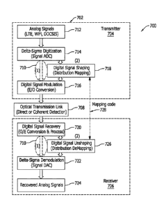
[0070] FIG. 7 is a schematic block diagram of an exemplary system-level
signal mapping process 700. In an exemplary embodiment, process 700 is
implemented
with respect to a coherent optical network system 702, which includes a
transmitter portion
704 and a receiver portion 706, in operable communication with each other over
an optical
transmission link 708 (e.g., for direct or coherent detection). In
the exemplary
embodiment, transmitter portion 704 represents the headend and or optical hub,
and
includes a complex, high speed ADC (not shown in FIG. 7), which is configured
to
perform the oversampling, noise shaping, and quantization (1-bit or 2-bit)
processes
described above to convert the analog input signals to digital outputs (00K or
PAM4,
respectively).
[0071] Also in an exemplary embodiment, receiver portion 706 includes a
fiber node and filters (also not shown in FIG. 7) configured to perform the
DAC processes
described above. As described above, process 700 differs from the conventional
Nyquist
ADC, which eliminates quantization noise by using many quantization bits. In
contrast,
process 700 may implement delta-sigma ADC to move the quantization noise out-
of-band.
Accordingly, a low-pass filter (LPF) or bandpass filter (BPF) may be
implemented on the
side of receiver portion 706 to filter out the desired signal. Simultaneously,
or at
CA 03050283 2019-07-15
WO 2018/136765 -20- PCT/US2018/014461
approximately the same time, the digitized signal may be converted back to its
analog
waveform by eliminating the out-of-band quantization noise. According to this
advantageous configuration, channel frequency demultiplexing and D/A
conversion may
both the implemented by a single device.
[0072] This asymmetry of the AD/DA operations of delta-sigma
digitization may be further advantageously implemented in point-to-multipoint
architectures, such as PONs, mobile fronthaul networks, and H.FC networks. In
an
exemplary embodiment, the complex ADC of process 700 may be centralized in the
headend/hub, and shared by multiple fiber nodes. In contrast, the simplified
LPF/BPF may
be distributed in each fiber node of optical link 708 to function as both the
DAC and
channel de-multiplexer. According to this advantageous system architecture,
the cost and
design complexity of fiber nodes may be significantly reduced, but while
improving system
reliability.
[0073] In an exemplary embodiment, process 700 is implemented with
respect to a DOCSIS 3.1 transmission. DOCSIS 3.1 utilizes OFDM signals, which
have a
continuous envelope and Gaussian-distributed amplitudes, i.e., there are more
small
amplitude samples than large amplitude samples. In the exemplary embodiment,
after 1-bit
delta-sigma digitization, the DOCSIS 3.1 signals are digitized to 00K signals.
Although
if, in this example, the number of 0 bits and 1 bits will be equal, there will
also occur many
consecutive Os or is due to the continuous envelope of input OFDM signals. To
improve
the transmission performance and facilitate the clock recovery of receiver
portion 706,
process 700 further implements symbol mapping to scramble the bit sequence and
thereby
avoid consecutive Os or is. Symbol matching may then be performed, and the
digitized
signal produced therefrom will have not only equal amount of 0 bits and 1
bits, but also
have Os and is therein evenly distributed in the transmitted time sequence.
[0074] Similarly, after 2-bit delta-sigma digitization, the DOCSIS 3.1
signals may be digitized to PAM4 signals using 4 symbols, i.e., 1 and 3. Due
to the
Gaussian distribution of the input analog signal (e.g., signal 216, FIG. 2),
the quantity of
these four symbols will also have a Gaussian distribution, i.e., there will be
more ls than
there will be 3s. As described further below, process 700 addresses this
distribution issue
by adjusting the symbol distribution of the digitized signals two more evenly
equalized the
CA 03050283 2019-07-15
WO 2018/136765 -21- PCT/US2018/014461
quantity of each symbol that is transmitted. According to these advantageous
techniques,
the present embodiments more fully utilize the capacity of the digital fiber
link (e.g., link
708), and maintain zero modification to the commercial DSP algorithms in
coherent/IM-
DD digital receivers. As described above, these techniques not limited to
DOCSIS 3.1, and
may be also applied to other transmitted signals, such as Wi-Fi, WiMAX, UWB,
LTE, and
5G wireless signals with the support of multicarrier modulation formats.
[0075] As described further below, process 700 implements mapping and
demapping flow techniques ("(2)") in in addition to the system flow 710
("(1)," dashed
circles) utilizing only the delta-sigma digitization techniques described
above. In the
exemplary embodiment, for an input analog signal 712, transmitter 704
implements a delta-
sigma digitization subprocess 714 to perform ADC on input analog signal 712.
When
implementing delta-sigma digitization without mapping, process 700 will
proceed from
delta-sigma digitization subprocess 714 to a digital signal modulation
subprocess 716 (e.g.,
E/O conversion). However, according to the exemplary embodiment, process 700
further
includes a digital signal shaping subprocess 718, performed after delta-sigma
digitization in
subprocess 714, but before digital signal modulation in subprocess 716, to
provide a
distribution mapping of the digitized signal on the transmitter side, i.e.,
transmitter portion
704.
[0076] In further operation, after modulation in subprocess 716, the
modulated signal is transmitted over optical transmission link 708. On the
receiver side,
i.e., receiver portion 706, process 700 then implements a digital signal
recovery subprocess
720 (e.g., 0/E conversion and processing). In the case where distribution
mapping has not
been implemented from subprocess 718, process 700 will proceed from recovery
subprocess 722 a delta-sigma demodulation subprocess 722, from which recovered
analog
signals 724 are obtained. However, according to the exemplary embodiment,
process 700
further includes a digital signal unshaping subprocess 726, performed after
digital signal
recovery in subprocess 720, but before delta-sigma demodulation in subprocess
722, to
provide a distribution demapping of the digitized signal on the receiver side,
i.e.,
transmitter portion 706, prior to analog conversion.
CA 03050283 2019-07-15
WO 2018/136765 -22- PCT/US2018/014461
[0077] In the exemplary embodiment, process 700 inserts a symbol
mapping subprocess (i.e., subprocess 718) on the transmitter side (i.e.,
transmitter portion
704) after delta-sigma digitization of input analog signal 712 in subprocess
714. Similarly,
process 700 employs a symbol demapping subprocess (i.e., subprocess 726) on
the receiver
side (i.e., receiver portion 706) to map/demap the signal back to the original
signal
sequences, and then feed the demapped signal into a DAC (i.e., delta-sigma
demodulation
subprocess 722) for digital-to-analog conversion. In the exemplary embodiment,
a
mapping code 728 is communicated from digital signal shaping subprocess 718 to
digital
signal unshaping process 726 to modify the signal distribution transmitted
over optical
transmission link 708. In some embodiments, mapping code 728 is transmitted
over
optical transmission link 708. In other embodiments, mapping code 728 is
transmitted over
alternative communication channels.
[0078] According to the exemplary configuration of process 700, because
the signal mapping/demapping subprocesses 718/726 are performed according to
their own
mapping code 728, the need is eliminated to modify existing commercial digital
signal
recovery algorithms after delta-sigma digitization is performed, or after the
signals are
transmitted over optical transmission link 708. In some embodiments, the
several
subprocesses of process 700 are performed by one or more hardware units (e.g.,
ADC,
DAC, modulator, demodulator, mapper, demapper) configured to perform one or
more of
the respective functions thereof. In other embodiments, the several
subprocesses are
implemented through software programming of at least one processor of
transmitter portion
704 and/or receiver portion 706. In at least one embodiment, the subprocesses
are
performed by a combination of hardware units and software programming. In an
exemplary embodiment, the DAC includes an LPF and/or a BPF.
[0079] FIG. 8 is a graphical illustration depicting an unmapped electrical
eye diagram 800 of a digitized signal after delta-sigma digitization (e.g.,
subprocess 714,
FIG. 7). In an exemplary embodiment, eye diagram 800 represents a PA1\44
signal after
delta-sigma digitization. In this example, the occurrence of +1 and -1 symbols
will each
have probabilities of pi, whereas the occurrence of +3 and -3 symbols Will
each have
probabilities of p3, and the total probabilities of all four symbols occurring
will be 100%.
CA 03050283 2019-07-15
WO 2018/136765 -23- PCT/US2018/014461
[0080] This total probability may be represented according to the
following equation:
2pi + 2193 = 100% (Eq. 1)
[0081] As described above, OFDM signals follow Gaussian distribution,
end result in more small amplitude samples than large amplitude samples.
Therefore, in
the digitized PAM4 signal, there are much more =1 symbols (small amplitude)
than =3
symbols (large amplitude), i.e. pr>> p3. Accordingly, as can be seen in eye
diagram 800,
areas 802 of greater intensity represent the =1 symbol levels, whereas areas
804 of lesser
intensity represent the +3 symbol levels, due to the unequal distribution.
[0082] FIG. 9 is a graphical illustration depicting an electrical eye diagram
900 of a digitized signal after delta-sigma digitization, implementing a flip
mapping
process. In this example, electrical eye diagram 900 represents the PAM4
signal of eye
diagram 800 after delta-sigma digitization, and after implementation of a flip
mapping
subprocess (described further below with respect to FIG. 10).
[0083] In the exemplary embodiment, the flip mapping subprocess of eye
diagram 900 maps the =1 symbols to the =3 symbols, but with the respective
sign
unchanged, and vice versa. That is, flip mapping of the symbols occurs as
follows: +3 4
+1; +1 4 +3; -1 -3; -3 -1. Accordingly, since pi>> p3, after flip
mapping, there will
be significantly more =3 symbols than =1 symbols. Accordingly, as can be seen
in eye
diagram 900, areas 902 of greater intensity represent the +3 symbol levels,
whereas areas
904 of lesser intensity represent the =1 symbol levels, in contrast to eye
diagram 800.
[0084] This reversal may be represented according to the following
equation:
yn = sgn(xn)(4 xn i) (Eq. 2)
[0085] Where xn is the symbol value of the digitized sequence of n
symbols, and ynis the symbol value of the digitized sequence after the flip
mapping
subprocess is implemented.
CA 03050283 2019-07-15
WO 2018/136765 -24- PCT/US2018/014461
[0086] FIG. 10 is a graphical illustration of a flip mapping table 1000 that
may be implemented with the digitized signal of electrical eye diagram 900,
FIG. 9. Flip
mapping table 1000 graphically illustrates the correspondence of flips of the
flip mapping
subprocess described above with respect to FIG. 9. In an exemplary embodiment,
flip
mapping table 1000 may be implemented in respective databases of the
transmitter (i.e.,
transmitter portion 704, FIG. 7) and the receiver (i.e., receiver portion 706,
FIG. 7) and
communicated therebetween as a code (i.e., mapping code 728, FIG. 7).
[0087] FIGS. 11A-B are graphical illustrations depicting a comparative
result of a transmitted signal with and without implementation of the flip
mapping
processes depicted in FIGS. 9 and 10. Specifically, FIG. 11A depicts a
transmitted signal
1100 upon which a delta-sigma digitization subprocess has been implemented,
but not a
mapping subprocess, and FIG. 11B depicts a mapped signal 1102, which
represents
transmitted signal 1100 after a flip mapping subprocess has been implemented
thereupon.
In this example, signals 1100, 1102 are illustrated as 16QAM 16GBaud signals
over a 40-
km transmission at 128Gb/s. Accordingly, as can be seen from a comparison of
mapped
signal 1102 with the transmitted (unmapped) signal 1100, the signal magnitude
smooths
significantly around the center frequency after implementation of the flip
mapping
subprocess.
[0088] FIGS. 12A-B are graphical illustrations depicting a comparative
result of a pseudorandom binary sequence (PRBS)-based PAM4 signal with a
result of a
signal upon which a unifoim mapping subprocess (subprocess A, described below)
has
been implemented. Specifically, FIG. 12A depicts an electrical eye diagram
1200 of a
PRBS-based PAM4 signal, and FIG. 12B depicts an electrical eye diagram 1202 of
a signal
implementing uniform mapping subprocess A.
[0089] In an exemplary embodiment, uniform mapping subprocess A
utilizes a scrambling code Sn, which represents a periodic pseudo-random bit
stream of 0
and 1 values with equal probabilities (i.e., 50 /a will be Os, and 50% will be
1s). For an
input symbol xn, the value will be flipped when Sn= 1, but remain unchanged
when Sn= 0.
Thus, uniform mapping subprocess A maybe implemented together with the flip
mapping
process described above with respect to FIGS. 9 and 10, above. Accordingly, as
can be
seen from a comparison of eye diagrams 1200 and 1202, after implementation of
uniform
CA 03050283 2019-07-15
WO 2018/136765 -25- PCT/US2018/014461
mapping subprocess A, the respective +1 and 3 symbols are equally
distributed. That is,
eye diagram 1202 of the mapped signal is almost identical with eye diagram
1200 of the
PRBS-based PAM4 signal.
[0090] FIGS. 13A-B are graphical illustrations of alternative symbol
mapping tables 1300 and 1302, respectively, that may be implemented with the
digitized
signal of electrical eye diagram 1202, FIG. 12B.
[0091] Symbol mapping table 1300 corresponds to uniform mapping
subprocess A, described above with respect to FIGS. 12A-B. In the exemplary
embodiment, utilizing scrambling code Sn, 50% of the +3 symbols will be mapped
to a +1
symbol (e.g., Sn= 1), whereas the other half of the +3 symbols will remain
unchanged (e.g.,
Sn= 0). The disposition of the +1, -1, and -3 symbols it will be deteunined
similarly, as
represented by the following equation for symbol mapping table 1300 (mapping
subprocess
A):
Yn
xn (Sn = 0)
= (Eq. 3)
{ sgn(xn)(4 ¨ lxõ D (sr, = 1)
[0092] Symbol mapping table 1302 is similar to symbol mapping table
1300, but utilizes an additional value for scrambling code S. That is,
according to symbol
mapping table 1302 (for uniform mapping subprocess "B"), scrambling code Sn
represents
a periodic pseudo-random bit stream of -1, 0, and 1 values with probabilities
of 25%, 50%
and 25%, respectively (i.e., (i.e., 25% of occurrences will be a -1, 50% of
occurrences will
be a 0, and 25 /0 of occurrences will be a 1). In this alternative embodiment,
for an input
symbol xn, the value will be flipped with its sign unchanged when Sn= 1, and
the value
will be flipped with its sign also flipped when when Sn= -1. When Sn= 0, both
the value
and the sign of xn remain unchanged.
[0093] The resulting values yn may be represented according to the
following equation:
1 xn (Sn = 0)
yn = sgn(xn)(4 ¨ Ixn1) (Sn = 1) (Eq. 4)
¨sgn(xn)(4 ¨ lxni) (Sn = ¨1)
CA 03050283 2019-07-15
WO 2018/136765 -26- PCT/US2018/014461
[0094] Looking specifically at the disposition of the +3 symbol, for
example, 25% of the +3 symbols will be mapped to a +1 symbol, another 25% of
the +3
symbols will be mapped to a -1 symbol, and the remaining 50% of the +3 symbols
remain
unchanged (i.e., mapped to a +3 symbol). The disposition of the +1, -1, and -3
symbols are
similarly deteimined according to the same calculations.
[0095] Similar to the implementation of uniform mapping subprocess A,
described above with respect to FIGS. 12A-B, implementation of uniform mapping
subprocess B also equally distributes the 1 and +3 symbols after mapping,
thereby
producing an eye diagram (not shown) that is also almost identical to eye
diagram 1200 of
the PRBS-based PAM4 signal. That is, an eye diagram produced according to
uniform
mapping subprocess B will be identical to eye diagram 1202 produced according
to
uniform mapping subprocess A (and therefore also to I diagram 1200 of the PRBS-
based
PAM4 signal). Accordingly, both uniform mapping subprocesses A and B May be
successfully implemented to modify the symbol distribution to map the
respective input
signal to a PRBS signal with the statistical accuracy.
[0096] FIGS. 14A-B are graphical illustrations depicting a comparative
result of a signal implementing the uniform mapping process depicted in FIG.
13A with a
signal implementing the alternative uniform mapping process depicted in FIG.
13B.
Specifically, FIG. 13A depicts a transmitted signal 1300 upon which uniform
mapping
subprocess A has been implemented, and FIG. 13B depicts a transmitted signal
1302 upon
which uniform mapping subprocess B has been implemented. In this example,
signal 1300
is illustrated as a 16QAM 16GBaud signal over a 40-km transmission at 128Gb/s,
and
signal 1302 is illustrated as a 16QAM 32GBaud signal over a 40-km transmission
at
256Gb/s. Accordingly, as can be seen from a comparison of signals 1300 and
1302, the
different uniform mapping subprocesses may be successfully implemented for
similar input
signals, but having different symbol rates and data rates.
[0097] FIG. 15 is a graphical illustration of a symbol table 1500
comparing the symbol mapping techniques of the several mapping subprocesses
described
above. In this example, the respective probabilities are labeled on each
mapping pass (i.e.,
"Matching A" for uniform mapping subprocess A, and "Matching B" for uniform
mapping
subprocess B), for each respective scrambling code Si, ("Scrambler A" and
"Scrambler
CA 03050283 2019-07-15
WO 2018/136765 -27- PCT/US2018/014461
B"). As can be seen from symbol table 1500, the respective probabilities of
symbol
occurrences change according to whether only a delta-sigma digitization
subprocess is
implemented on the analog signal, or whether a flip mapping subprocess, and or
a two-
value or a three-value uniform mapping/scrambling subprocess is also
implemented. As
described with respect to the embodiments above, the mapping and demapping
techniques
of the present systems and methods significantly improve the quality and
capability of a
digitized signal transmitted over an optical link.
[0098] Although specific features of various embodiments of the
disclosure may be shown in some drawings and not in others, this is for
convenience only.
In accordance with the principles of the disclosure, a particular feature
shown in a drawing
may be referenced and/or claimed in combination with features of the other
drawings. For
example, the following list of example claims represents only some of the
potential
combinations of elements possible from the systems and methods described
herein.
[0099] a(i). An optical network, comprising: a transmitter
portion
configured to transmit a digitized stream of symbols over a digital optical
link; a mapping
unit disposed within the transmitter portion and configured to code the
transmitted digitized
stream of symbols with a mapping code prior to transmission over the digital
optical link; a
receiver portion configured to recover the coded stream of symbols from the
digital optical
link; and a demapping unit disposed within the receiver portion and configured
to map the
recovered coded stream of symbols into an uncoded digitized signal
corresponding to the
digitized stream of symbols at the transmitter portion prior to coding by the
mapping unit.
[00100] b(i). The system of claim a(i), wherein the transmitter portion
comprises an analog-to-digital converter configured to digitize an input
analog signal.
[00101] c(i). The system of claim b(i), wherein the analog-to-digital
converter is configured to implement delta-sigma digitization on the input
analog signal.
[00102] d(i). The system of claim c(i), wherein the analog-to-digital
converter is disposed within the transmitter portion such that the delta-sigma
digitization of
the input analog signal is implemented prior to coding of the transmitted
digitized stream
by the mapping unit.
CA 03050283 2019-07-15
WO 2018/136765 -28- PCT/US2018/014461
[00103] e(i). The system of claim c(i), wherein the receiver portion
comprises an digital-to-analog converter configured to convert the uncoded
digitized signal
into a recovered analog signal.
[00104] f(i). The system of claim e(i), wherein the digital-to-analog
converter is configured to implement delta-sigma demodulation on the uncoded
digitized
signal.
[00105] g(i). The system of claim f(i), wherein the digital-to-analog
converter is disposed within the receiver portion such that the delta-sigma
demodulation of
the uncoded digitized signal is implemented after mapping of the recovered
coded stream
by the demapping unit.
[00106] h(i). The system of claim a(i), wherein the system is configured
to transmit a signal according to one or more of a DOCSIS 3.1, a Wi-Fi, a
WiMAX, a
UWB, an LTE, and a 5G wireless signal specification.
[00107] i(i). The system of claim a(i), wherein the digitized stream of
symbols is digitized according to at least one of an OOK and a PAM4 signal
format.
[00108] a(ii). A symbol mapping method for a digitized signal, the
digitized signal including a series of transmitted symbols having a Gaussian
distribution of
symbol amplitude values, the method comprising the steps of: mapping, for at
least one
input occurrence of a first symbol of the series of transmitted symbols, the
first symbol to a
second symbol of the series of transmitted symbols, wherein the first symbol
has a first
symbol amplitude value and the second symbol as a second symbol amplitude
value greater
than the first symbol amplitude value; and mapping, for at least one
occurrence of the
second symbol, the second symbol to the first symbol.
[00109] b(ii). The method of claim a(ii), wherein the sign of the first and
second symbols remains unchanged after mapping to the other of the first and
second
symbols.
[00110] c(ii). The method of claim a(ii), further comprising the step of
applying a scrambling code to each input occurrence of the first and second
symbols.
CA 03050283 2019-07-15
WO 2018/136765 -29- PCT/US2018/014461
[00111] d(ii). The method of claim c(ii), wherein the scrambling code
comprises a periodic pseudo-random bit stream of 0 and 1 values having
substantially
equal probabilities of occurrence.
[00112] e(ii). The method of claim d(ii), wherein, for each occurrence of
the first input symbol, the first symbol is mapped to the second symbol when
the
scrambling code has a 1 value, and the first symbol remains unchanged when the
scrambling code has a 0 value.
[00113] f(ii). The method of claim c(ii), wherein the scrambling code
comprises a periodic pseudo-random bit stream of -1, 0, and 1 values, wherein
the -1 and 1
values each have a 25% probability of occurrence, and wherein the 0 value has
a 50%
probability of occurrence.
[00114] g(ii). The method of claim f(ii), wherein, for each occurrence of
the first input symbol, the first symbol is mapped to the second symbol when
the
scrambling code has a -1 or 1 value, and the first symbol remains unchanged
when the
scrambling code has a 0 value.
[00115] h(ii). The method of claim g(ii), wherein, for each mapping of
the first symbol to the second symbol, the symbol amplitude value of the
mapped first
symbol will be equal to the symbol amplitude value of the second symbol, the
sign of the
mapped first symbol will remain unchanged when the scrambling code has a 1
value, and
the sign of the mapped first symbol will be reversed when the scrambling code
has a -1
value.
[00116] i(ii). The method of claim a(ii), wherein the first symbol has a 1
value in the second symbol has a 3 value.
[00117] j(ii). The method of claim a(ii), wherein the series of transmitted
symbols represents a PAM4 signal.
[00118] k(ii). The method of claim a(ii), wherein the digitized signal is a
DOCSIS 3.1 signal.
CA 03050283 2019-07-15
WO 2018/136765 -30- PCT/US2018/014461
[00119] Some embodiments involve the use of one or more electronic or
computing devices. Such devices typically include a processor or controller,
such as a
general purpose central processing unit (CPU), a graphics processing unit
(GPU), a
microcontroller, a reduced instruction set computer (RISC) processor, an
application
specific integrated circuit (ASIC), a programmable logic circuit (PLC), a
field
programmable gate array (FPGA), a DSP device, and/or any other circuit or
processor
capable of executing the functions described herein. The processes described
herein may
be encoded as executable instructions embodied in a computer readable medium,
including,
without limitation, a storage device and/or a memory device. Such
instructions, when
executed by a processor, cause the processor to perform at least a portion of
the methods
described herein. The above examples are exemplary only, and thus are not
intended to
limit in any way the definition and/or meaning of the term "processor."
[00120] This written description uses examples to disclose the
embodiments, including the best mode, and also to enable any person skilled in
the art to
practice the embodiments, including making and using any devices or systems
and
performing any incorporated methods. The patentable scope of the disclosure is
defined by
the claims, and may include other examples that occur to those skilled in the
art. Such
other examples are intended to be within the scope of the claims if they have
structural
elements that do not differ from the literal language of the claims, or if
they include
equivalent structural elements with insubstantial differences from the literal
language of the
claims.