Note: Descriptions are shown in the official language in which they were submitted.
CA 03051248 2019-07-22
WO 2018/144639
PCT/US2018/016300
REDUCING OSCILLATION IN A SIGNAL BOOSTER
BACKGROUND
[0001] Signal boosters and repeaters can be used to increase the quality of
wireless
communication between a wireless device and a wireless communication access
point,
such as a cell tower. Signal boosters can improve the quality of the wireless
communication by amplifying, filtering, and/or applying other processing
techniques to
uplink and downlink signals communicated between the wireless device and the
wireless
communication access point.
[0002] As an example, the signal booster can receive, via an antenna, downlink
signals
from the wireless communication access point. The signal booster can amplify
the
downlink signal and then provide an amplified downlink signal to the wireless
device. In
other words, the signal booster can act as a relay between the wireless device
and the
wireless communication access point. As a result, the wireless device can
receive a
stronger signal from the wireless communication access point. Similarly,
uplink signals
from the wireless device (e.g., telephone calls and other data) can be
directed to the signal
booster. The signal booster can amplify the uplink signals before
communicating, via an
antenna, the uplink signals to the wireless communication access point.
BRIEF DESCRIPTION OF THE DRAWINGS
[0003] Features and advantages of the disclosure will be apparent from the
detailed
description which follows, taken in conjunction with the accompanying
drawings, which
together illustrate, by way of example, features of the disclosure; and,
wherein:
[0004] FIG. 1 illustrates a signal booster in communication with a wireless
device and a
base station in accordance with an example;
[0005] FIG 2 illustrates a cellular signal booster configured to amplify
uplink (UL) and
downlink (DL) signals using one or more downlink signal paths and one or more
uplink
signal paths in accordance with an example;
[0006] FIG. 3 illustrates a signal booster with a controller operable to
reduce oscillation in
the signal booster in accordance with an example;
1
CA 03051248 2019-07-22
WO 2018/144639
PCT/US2018/016300
[0007] FIG. 4 illustrates a technique for reducing oscillation in a signal
booster in
accordance with an example;
[0008] FIG. 5 illustrates a technique for reducing oscillation in a signal
booster in
accordance with an example; and
[0009] FIG 6 illustrates a wireless device in accordance with an example.
[0010] Reference will now be made to the exemplary embodiments illustrated,
and
specific language will be used herein to describe the same. It will
nevertheless be
understood that no limitation of the scope of the invention is thereby
intended.
DETAILED DESCRIPTION
[0011] Before the present invention is disclosed and described, it is to be
understood that
this invention is not limited to the particular structures, process steps, or
materials
disclosed herein, but is extended to equivalents thereof as would be
recognized by those
ordinarily skilled in the relevant arts. It should also be understood that
terminology
employed herein is used for the purpose of describing particular examples only
and is not
intended to be limiting. The same reference numerals in different drawings
represent the
same element. Numbers provided in flow charts and processes are provided for
clarity in
illustrating steps and operations and do not necessarily indicate a particular
order or
sequence.
EXAMPLE EMBODIMENTS
[0012] An initial overview of technology embodiments is provided below and
then
specific technology embodiments are described in further detail later. This
initial
summary is intended to aid readers in understanding the technology more
quickly but is
not intended to identify key features or essential features of the technology
nor is it
intended to limit the scope of the claimed subject matter.
[0013] FIG. 1 illustrates an exemplary signal booster 120 in communication
with a
wireless device 110 and a base station 130. The signal booster 120 can be
referred to as a
repeater. A repeater can be an electronic device used to amplify (or boost)
signals. The
signal booster 120 (also referred to as a cellular signal amplifier) can
improve the quality
2
CA 03051248 2019-07-22
WO 2018/144639
PCT/US2018/016300
of wireless communication by amplifying, filtering, and/or applying other
processing
techniques via a signal amplifier 122 to uplink signals communicated from the
wireless
device 110 to the base station 130 and/or downlink signals communicated from
the base
station 130 to the wireless device 110. In other words, the signal booster 120
can amplify
.. or boost uplink signals and/or downlink signals bi-directionally. In one
example, the
signal booster 120 can be at a fixed location, such as in a home or office.
Alternatively,
the signal booster 120 can be attached to a mobile object, such as a vehicle
or a wireless
device 110.
[0014] In one configuration, the signal booster 120 can include an integrated
device
antenna 124 (e.g., an inside antenna or a coupling antenna) and an integrated
node
antenna 126 (e.g., an outside antenna). The integrated node antenna 126 can
receive the
downlink signal from the base station 130. The downlink signal can be provided
to the
signal amplifier 122 via a second coaxial cable 127 or other type of radio
frequency
connection operable to communicate radio frequency signals. The signal
amplifier 122
can include one or more cellular signal amplifiers for amplification and
filtering. The
downlink signal that has been amplified and filtered can be provided to the
integrated
device antenna 124 via a first coaxial cable 125 or other type of radio
frequency
connection operable to communicate radio frequency signals. The integrated
device
antenna 124 can wirelessly communicate the downlink signal that has been
amplified and
filtered to the wireless device 110.
[0015] Similarly, the integrated device antenna 124 can receive an uplink
signal from the
wireless device 110. The uplink signal can be provided to the signal amplifier
122 via the
first coaxial cable 125 or other type of radio frequency connection operable
to
communicate radio frequency signals. The signal amplifier 122 can include one
or more
.. cellular signal amplifiers for amplification and filtering. The uplink
signal that has been
amplified and filtered can be provided to the integrated node antenna 126 via
the second
coaxial cable 127 or other type of radio frequency connection operable to
communicate
radio frequency signals. The integrated device antenna 126 can communicate the
uplink
signal that has been amplified and filtered to the base station 130.
[0016] In one example, the signal booster 120 can filter the uplink and
downlink signals
using any suitable analog or digital filtering technology including, but not
limited to,
3
CA 03051248 2019-07-22
WO 2018/144639
PCT/US2018/016300
surface acoustic wave (SAW) filters, bulk acoustic wave (BAW) filters, film
bulk acoustic
resonator (FBAR) filters, ceramic filters, waveguide filters or low-
temperature co-fired
ceramic (LTCC) filters.
[0017] In one example, the signal booster 120 can send uplink signals to a
node and/or
receive downlink signals from the node. The node can comprise a wireless wide
area
network (WWAN) access point (AP), a base station (BS), an evolved Node B
(eNB), a
baseband unit (BBU), a remote radio head (RRH), a remote radio equipment
(RRE), a
relay station (RS), a radio equipment (RE), a remote radio unit (RRU), a
central
processing module (CPM), or another type of WWAN access point.
[0018] In one configuration, the signal booster 120 used to amplify the uplink
and/or a
downlink signal is a handheld booster. The handheld booster can be implemented
in a
sleeve of the wireless device 110. The wireless device sleeve can be attached
to the
wireless device 110, but can be removed as needed. In this configuration, the
signal
booster 120 can automatically power down or cease amplification when the
wireless
device 110 approaches a particular base station. In other words, the signal
booster 120 can
determine to stop performing signal amplification when the quality of uplink
and/or
downlink signals is above a defined threshold based on a location of the
wireless device
110 in relation to the base station 130.
[0019] In one example, the signal booster 120 can include a battery to provide
power to
various components, such as the signal amplifier 122, the integrated device
antenna 124
and the integrated node antenna 126. The battery can also power the wireless
device 110
(e.g., phone or tablet). Alternatively, the signal booster 120 can receive
power from the
wireless device 110.
[0020] In one configuration, the signal booster 120 can be a Federal
Communications
.. Commission (FCC)-compatible consumer signal booster. As a non-limiting
example, the
signal booster 120 can be compatible with FCC Part 20 or 47 Code of Federal
Regulations (C.F.R.) Part 20.21 (March 21, 2013). In addition, the signal
booster 120 can
operate on the frequencies used for the provision of subscriber-based services
under parts
22 (Cellular), 24 (Broadband PCS), 27 (AWS-1, 700 MHz Lower A-E Blocks, and
700
MHz Upper C Block), and 90 (Specialized Mobile Radio) of 47 C.F.R. The signal
booster
120 can be configured to automatically self-monitor its operation to ensure
compliance
4
CA 03051248 2019-07-22
WO 2018/144639
PCT/US2018/016300
with applicable noise and gain limits. The signal booster 120 can either self-
correct or
shut down automatically if the signal booster's operations violate the
regulations defined
in FCC Part 20.21.
[0021] In one configuration, the signal booster 120 can improve the wireless
connection
between the wireless device 110 and the base station 130 (e.g., cell tower) or
another type
of wireless wide area network (WWAN) access point (AP). The signal booster 120
can
boost signals for cellular standards, such as the Third Generation Partnership
Project
(3GPP) Long Term Evolution (LTE) Release 8, 9, 10, 11, 12, or 13 standards or
Institute
of Electronics and Electrical Engineers (IEEE) 802.16. In one configuration,
the signal
booster 120 can boost signals for 3GPP LTE Release 13Ø0 (March 2016) or
other
desired releases. The signal booster 120 can boost signals from the 3GPP
Technical
Specification 36.101 (Release 12 Jun 2015) bands or LTE frequency bands. For
example,
the signal booster 120 can boost signals from the LTE frequency bands: 2, 4,
5, 12, 13,
17, and 25. In addition, the signal booster 120 can boost selected frequency
bands based
on the country or region in which the signal booster is used, including any of
bands 1-70
or other bands, as disclosed in ETSI T5136 104 V13.5.0 (2016-10).
[0022] The number of LTE frequency bands and the level of signal improvement
can vary
based on a particular wireless device, cellular node, or location. Additional
domestic and
international frequencies can also be included to offer increased
functionality. Selected
models of the signal booster 120 can be configured to operate with selected
frequency
bands based on the location of use. In another example, the signal booster 120
can
automatically sense from the wireless device 110 or base station 130 (or GPS,
etc.) which
frequencies are used, which can be a benefit for international travelers.
[0023] In one example, the integrated device antenna 124 and the integrated
node antenna
126 can be comprised of a single antenna, an antenna array, or have a
telescoping form-
factor. In another example, the integrated device antenna 124 and the
integrated node
antenna 126 can be a microchip antenna. An example of a microchip antenna is
AMMAL001. In yet another example, the integrated device antenna 124 and the
integrated node antenna 126 can be a printed circuit board (PCB) antenna. An
example of
a PCB antenna is TE 2118310-1.
[0024] In one example, the integrated device antenna 124 can receive uplink
(UL) signals
5
CA 03051248 2019-07-22
WO 2018/144639
PCT/US2018/016300
from the wireless device 110 and transmit DL signals to the wireless device
110 using a
single antenna. Alternatively, the integrated device antenna 124 can receive
UL signals
from the wireless device 110 using a dedicated UL antenna, and the integrated
device
antenna 124 can transmit DL signals to the wireless device 110 using a
dedicated DL
antenna.
[0025] In one example, the integrated device antenna 124 can communicate with
the
wireless device 110 using near field communication. Alternatively, the
integrated device
antenna 124 can communicate with the wireless device 110 using far field
communication.
[0026] In one example, the integrated node antenna 126 can receive downlink
(DL)
signals from the base station 130 and transmit uplink (UL) signals to the base
station 130
via a single antenna. Alternatively, the integrated node antenna 126 can
receive DL
signals from the base station 130 using a dedicated DL antenna, and the
integrated node
antenna 126 can transmit UL signals to the base station 130 using a dedicated
UL
antenna.
[0027] In one configuration, multiple signal boosters can be used to amplify
UL and DL
signals. For example, a first signal booster can be used to amplify UL signals
and a
second signal booster can be used to amplify DL signals. In addition,
different signal
boosters can be used to amplify different frequency ranges.
[0028] In one configuration, the signal booster 120 can be configured to
identify when
the wireless device 110 receives a relatively strong downlink signal. An
example of a
strong downlink signal can be a downlink signal with a signal strength greater
than
approximately -80dBm. The signal booster 120 can be configured to
automatically turn
off selected features, such as amplification, to conserve battery life. When
the signal
booster 120 senses that the wireless device 110 is receiving a relatively weak
downlink
signal, the integrated booster can be configured to provide amplification of
the downlink
signal. An example of a weak downlink signal can be a downlink signal with a
signal
strength less than -80dBm.
[0029] In one example, the signal booster 120 can also include one or more of:
a
waterproof casing, a shock absorbent casing, a flip-cover, a wallet, or extra
memory
storage for the wireless device. In one example, extra memory storage can be
achieved
6
CA 03051248 2019-07-22
WO 2018/144639
PCT/US2018/016300
with a direct connection between the signal booster 120 and the wireless
device 110. In
another example, Near-Field Communications (NFC), Bluetooth v4.0, Bluetooth
Low
Energy, Bluetooth v4.1, Bluetooth v4.2, Bluetooth 5, Ultra High Frequency
(UHF), 3GPP
LTE, Institute of Electronics and Electrical Engineers (IEEE) 802.11a, IEEE
802.11b,
IEEE 802.11g, IEEE 802.11n, IEEE 802.11ac, or IEEE 802.11ad can be used to
couple
the signal booster 120 with the wireless device 110 to enable data from the
wireless
device 110 to be communicated to and stored in the extra memory storage that
is
integrated in the signal booster 120. Alternatively, a connector can be used
to connect the
wireless device 110 to the extra memory storage.
[0030] In one example, the signal booster 120 can include photovoltaic cells
or solar
panels as a technique of charging the integrated battery and/or a battery of
the wireless
device 110. In another example, the signal booster 120 can be configured to
communicate
directly with other wireless devices with signal boosters. In one example, the
integrated
node antenna 126 can communicate over Very High Frequency (VHF) communications
directly with integrated node antennas of other signal boosters. The signal
booster 120
can be configured to communicate with the wireless device 110 through a direct
connection, Near-Field Communications (NFC), Bluetooth v4.0, Bluetooth Low
Energy,
Bluetooth v4.1, Bluetooth v4.2, Ultra High Frequency (UHF), 3GPP LTE,
Institute of
Electronics and Electrical Engineers (IEEE) 802.11a, IEEE 802.11b, IEEE
802.11g, IEEE
802.11n, IEEE 802.11ac, IEEE 802.11ad, a TV White Space Band (TVWS), or any
other
industrial, scientific and medical (ISM) radio band. Examples of such ISM
bands include
2.4 GHz, 3.6 GHz, 4.9 GHz, 5 GHz, or 5.9 GHz. This configuration can allow
data to
pass at high rates between multiple wireless devices with signal boosters.
This
configuration can also allow users to send text messages, initiate phone
calls, and engage
.. in video communications between wireless devices with signal boosters. In
one example,
the integrated node antenna 126 can be configured to couple to the wireless
device 110. In
other words, communications between the integrated node antenna 126 and the
wireless
device 110 can bypass the integrated booster.
[0031] In another example, a separate VHF node antenna can be configured to
.. communicate over VHF communications directly with separate VHF node
antennas of
other signal boosters. This configuration can allow the integrated node
antenna 126 to be
used for simultaneous cellular communications. The separate VHF node antenna
can be
7
CA 03051248 2019-07-22
WO 2018/144639
PCT/US2018/016300
configured to communicate with the wireless device 110 through a direct
connection,
Near-Field Communications (NFC), Bluetooth v4.0, Bluetooth Low Energy,
Bluetooth
v4.1, Bluetooth v4.2, Ultra High Frequency (UHF), 3GPP LTE, Institute of
Electronics
and Electrical Engineers (IEEE) 802.11a, IEEE 802.11b, IEEE 802.11g, IEEE
802.11n,
.. IEEE 802.11ac, IEEE 802.11ad, a TV White Space Band (TVWS), or any other
industrial,
scientific and medical (ISM) radio band.
[0032] In one configuration, the signal booster 120 can be configured for
satellite
communication. In one example, the integrated node antenna 126 can be
configured to act
as a satellite communication antenna. In another example, a separate node
antenna can be
used for satellite communications. The signal booster 120 can extend the range
of
coverage of the wireless device 110 configured for satellite communication.
The
integrated node antenna 126 can receive downlink signals from satellite
communications
for the wireless device 110. The signal booster 120 can filter and amplify the
downlink
signals from the satellite communication. In another example, during satellite
communications, the wireless device 110 can be configured to couple to the
signal
booster 120 via a direct connection or an ISM radio band. Examples of such ISM
bands
include 2.4 GHz, 3.6 GHz, 4.9 GHz, 5 GHz, or 5.9 GHz.
[0033] FIG. 2 illustrates an exemplary bi-directional wireless signal booster
200
configured to amplify uplink (UL) and downlink (DL) signals using a separate
signal path
for each UL frequency band and DL frequency band and a controller 240. The bi-
directional wireless signal booster 200 can be integrated with a GPS module in
a signal
booster. An outside antenna 210, or an integrated node antenna, can receive a
downlink
signal. For example, the downlink signal can be received from a base station
(not shown).
The downlink signal can be provided to a first B1/B2 diplexer 212, wherein B1
represents
.. a first frequency band and B2 represents a second frequency band. The first
B1/B2
diplexer 212 can create a B1 downlink signal path and a B2 downlink signal
path.
Therefore, a downlink signal that is associated with B1 can travel along the
B1 downlink
signal path to a first B1 duplexer 214, or a downlink signal that is
associated with B2 can
travel along the B2 downlink signal path to a first B2 duplexer 216. After
passing the first
B1 duplexer 214, the downlink signal can travel through a series of amplifiers
(e.g., A10,
All and Al2) and downlink band pass filters (BPF) to a second B1 duplexer 218.
Alternatively, after passing the first B2 duplexer 216, the downlink can
travel through a
8
CA 03051248 2019-07-22
WO 2018/144639
PCT/US2018/016300
series of amplifiers (e.g., A07, A08 and A09) and downlink band pass filters
(BFF) to a
second B2 duplexer 220. At this point, the downlink signal (B1 or B2) has been
amplified
and filtered in accordance with the type of amplifiers and BPFs included in
the bi-
directional wireless signal booster 200. The downlink signals from the second
B1
.. duplexer 218 or the second B2 duplexer 220, respectively, can be provided
to a second
B1/B2 diplexer 222. The second B1/B2 diplexer 222 can provide an amplified
downlink
signal to an inside antenna 230, or an integrated device antenna. The inside
antenna 230
can communicate the amplified downlink signal to a wireless device (not
shown), such as
a mobile phone.
[0034] In one example, the inside antenna 230 can receive an uplink (UL)
signal from the
wireless device. The uplink signal can be provided to the second B1/B2
diplexer 222. The
second B1/B2 diplexer 222 can create a B1 uplink signal path and a B2 uplink
signal
path. Therefore, an uplink signal that is associated with B1 can travel along
the B1 uplink
signal path to the second B1 duplexer 218, or an uplink signal that is
associated with B2
.. can travel along the B2 uplink signal path to the second B2 duplexer 222.
After passing
the second B1 duplexer 218, the uplink signal can travel through a series of
amplifiers
(e.g., A01, A02 and A03) and uplink band pass filters (BPF) to the first B1
duplexer 214.
Alternatively, after passing the second B2 duplexer 220, the uplink signal can
travel
through a series of amplifiers (e.g., A04, A05 and A06) and uplink band pass
filters (BPF)
to the first B2 duplexer 216. At this point, the uplink signal (B1 or B2) has
been amplified
and filtered in accordance with the type of amplifiers and BFFs included in
the bi-
directional wireless signal booster 200. The uplink signals from the first B1
duplexer 214
or the first B2 duplexer 216, respectively, can be provided to the first Bl/B2
diplexer 12.
The first Bl/B2 diplexer 212 can provide an amplified uplink signal to the
outside
antenna 210. The outside antenna can communicate the amplified uplink signal
to the
base station.
[0035] In one example, the bi-directional wireless signal booster 200 can be a
6-band
booster. In other words, the bi-directional wireless signal booster 200 can
perform
amplification and filtering for downlink and uplink signals having a frequency
in bands
Bl, B2, B3 B4, B5 and/or B6.
[0036] In one example, the bi-directional wireless signal booster 200 can use
the
9
CA 03051248 2019-07-22
WO 2018/144639
PCT/US2018/016300
duplexers to separate the uplink and downlink frequency bands, which are then
amplified
and filtered separately. A multiple-band cellular signal booster can typically
have
dedicated radio frequency (RF) amplifiers (gain blocks), RF detectors,
variable RF
attenuators and RF filters for each uplink and downlink band.
.. [0037] FIG. 3 illustrates an example of a signal booster 300. The signal
booster 300 can
also be referred to as a repeater. The signal booster 300 can include a first
antenna (or
inside antenna 310) and a second antenna (or outside antenna 320). The signal
booster
300 can include a first multi-band filter 312 and a second multi-band filter
322. The first
multi-band filter 312 can be communicatively coupled between the first antenna
(or inside
antenna 310) and the second antenna (or outside antenna 320), and the second
multi-band
filter 322 can be communicatively coupled between the first antenna (or inside
antenna
310) and the second antenna (or outside antenna 320). The first multi-band
filter 312 and
the second multi-band filter 322 can include splitters, duplexers, triplexers,
quad-plexers,
etc.
[0038] In one example, the signal booster 300 can include one or more
amplification and
filtering signal paths. For example, the signal booster 300 can include one or
more uplink
amplification and filtering signal paths, and the signal booster 300 can
include one or
more downlink amplification and filtering signal paths. Each amplification and
filtering
signal path (either uplink or downlink) can include one or more amplifiers and
one or
more filters to manipulate the signals.
[0039] In one configuration, the signal booster 300 can include a controller
340. The
controller 340 can be configured to reduce oscillation in the signal booster
300. Generally
speaking, the oscillation can be created when outside and inside antennas that
are
internally located in the signal booster 300 are within a defined distance
from each other,
such that a level of booster amplification is greater than a path loss between
the antennas
and a positive feedback loop exists. With signal boosters, two antennas that
are within a
defined distance from each other can produce an RF squeal.
[0040] From an installation perspective, a customer may install signal booster
antennas
relatively close to each other (e.g., due to constraints in a home), but a
greater gain of the
signal booster requires that the antennas be installed further away from each
other. When
antennas are installed relatively close to each other, the oscillation can
occur in either a
CA 03051248 2019-07-22
WO 2018/144639
PCT/US2018/016300
downlink path or an uplink path. In some cases, downlink and/or uplink signals
can be
analyzed to determine the presence of or confirm an oscillation created by an
amplifier in
the signal booster.
[0041] In one example, oscillations can be caused due to feedback or noise,
which can be
amplified in the signal booster 300 over a period of time. Since the signal
booster 300 can
include both an uplink path and a downlink path, there is a loop that has the
potential to
cause internal oscillations. For example, in a feedback path from one antenna
to another
antenna, one antenna can transmit to the other antenna. An oscillation can
occur when a
loss between antennas is less than a gain in the signal booster 300. An
oscillation may not
occur when a loss between the antennas is greater than a gain in the signal
booster 300. In
addition, an oscillation can occur when an output port of the signal booster
300 couples
back to an input port of the signal booster due to poor shielding.
[0042] In one example, the signal booster 300 can include the first antenna
(or inside
antenna 310), the one or more amplifiers, the second antenna (or outside
antenna 320),
and cabling that connects the first antenna (or inside antenna 310), the one
or more
amplifiers, and the second antenna (or outside antenna 320). The second
antenna (or
outside antenna 320) can receive a signal outside a building and transmit the
signal to the
one or more amplifiers. The one or more amplifier can boost the signal and
then send an
amplified signal to the first antenna (or inside antenna 310). The first
antenna (or inside
antenna 310) can broadcast the amplified signal to an area with poor signal
coverage. An
oscillation can occur when a broadcasted signal from the first antenna (or
inside antenna
310) is detected by the second antenna (or outside antenna 320), and the
broadcasted
signal is passed through the signal booster 300 again, which can result in a
background
noise. This noise can result in poor reception on the device being used. In
some cases, the
signal booster 300 can automatically reduce their capabilities or shut down
when an
oscillation or feedback begins to occur.
[0043] In one configuration, the controller 340 can detect an oscillation in
the signal
booster 300. The controller 340 can reduce a gain in the signal booster 300 by
a first
amount to cease the oscillation in the signal booster 300. In other words, the
oscillation
can be stopped by reducing the gain by the first amount in the signal booster
300 to an
oscillation threshold level at which oscillation begins. This level can be a
predetermined
11
CA 03051248 2019-07-22
WO 2018/144639
PCT/US2018/016300
threshold level based on certain non-linearities that occur in oscillation.
For example,
when an input gain is increased by a predetermined amount, and the output gain
is greater
than the input. In another example, a noise floor level can increase by a non-
linear
amount relative to an input gain. The controller 340 can reduce the gain in
the signal
booster 300 further, below the oscillation threshold, by a second amount to
create an
oscillation margin. The oscillation margin can be a margin between an
operating gain of
the signal booster 300 and a gain at which oscillation begins (the oscillation
threshold) in
the signal booster 300. The oscillation margin can ensure that a noise floor
does not rise
above a level allowed by the set oscillation margin. The controller 340 can
modify (e.g.,
reduce) the gain in the signal booster 300 further by a third amount to create
an offset to
the oscillation margin. In other words, the offset can create an additional
margin to the
oscillation margin. In effect, the oscillation margin can be increased by the
offset (based
on the reduction of the gain in the signal booster 300 by the third amount).
The first
amount, the second amount and the third amount can be represented in decibels
(dB). In
addition, the offset to the oscillation margin can reduce a transmitted noise
power from
the signal booster 300. The transmitted noise power can increase as the signal
booster 300
gets closer to oscillation, so the offset to the oscillation margin can
function to reduce the
transmitted noise power.
[0044] In one example, the controller 340 can periodically increase the gain
in the signal
booster 300. The offset to the oscillation margin can reduce a likelihood that
the increase
to the gain causes a subsequent oscillation at the signal booster 300. In
addition, the gain
can be periodically increased to confirm an existence of the oscillation
margin. In other
words, the gain can be periodically increased to confirm an expected
oscillation margin.
In one example, the controller 340 can increase the gain by the oscillation
margin. In
another example, the controller 340 can increase the gain by the offset to the
oscillation
margin. In yet another example, the controller 340 can increase the gain by
the oscillation
margin and the offset to the oscillation margin.
[0045] In one configuration, the controller 340 can create an offset to the
oscillation
margin, which can further minimize the noise floor impact of the signal
booster 300. The
creation of the offset to the oscillation margin can be implemented in
firmware. The
creation of the offset to the oscillation margin can be more accurate under
stable antenna
feedback conditions (e.g., when the antennas and environment are not moving).
In one
12
CA 03051248 2019-07-22
WO 2018/144639
PCT/US2018/016300
configuration, the controller 340 can determine and add an oscillation margin
(e.g., a first
margin relative to the oscillation threshold level). Then, the controller 340
can add an
additional margin (e.g., a second margin relative to the first margin) on top
of the
oscillation margin (or first margin). The additional margin (e.g., the second
margin) can
also be referred to as the offset to the oscillation margin or the additional
margin to the
oscillation margin (e.g., the first margin).
[0046] In one example, the gain can be periodically increased to ensure that
the signal
booster 300 has a proper margin. The feedback path can be changed due to a
variety of
issues, such as time, temperature, objects moving around, a vehicle or the
mobile device
moving around, etc. The feedback path can be changed when antenna becomes
bumped or
moved. Therefore, to ensure that the oscillation margin (e.g., 5 dB) is still
present (and is
at an expected level), the signal booster can be periodically bumped up (i.e.,
the gain can
be increased to remove the oscillation margin). In other words, the signal
booster 300 can
periodically remove the oscillation margin to ensure that the oscillation
margin is still
accurate, and this can be referred to as a `bump-up', and the noise floor can
increase
during bump-up.
[0047] The amount of amplification applied by a signal booster can change due
to a
number of factors, including changes in the atmosphere, movement of objects
around the
antennas, movement of the antennas, movement of the wireless device, and so
forth. The
periodic bump-up (or increase of the gain in the signal booster) can function
to remove
the oscillation margin (e.g., the first margin) to ensure that the signal
booster 300 is still
operating within the oscillation margin (e.g., the first margin). By adding
the second
margin, it reduces the chances that the signal booster will be operating at or
above the
oscillation threshold level when the bump-up is applied. Accordingly, when the
bump-up
is applied, the noise floor increase can be reduced by adding the additional
margin (e.g.,
the second margin) to the oscillation margin (e.g., the first margin) since
non-linear
increases in noise floor will be reduced by maintaining the second margin
below the
oscillation threshold level.
[0048] In another example, the controller 340 can confirm that the additional
margin
(e.g., the second margin) is still accurate with a less frequent bump-up that
removes both
the oscillation margin (e.g., the first margin) and the additional margin
(e.g., the second
13
CA 03051248 2019-07-22
WO 2018/144639
PCT/US2018/016300
margin). By operating the signal booster near, at, or above the oscillation
threshold level
less frequently, the amplifiers operating in the signal booster can have a
longer operating
life. In addition, power use can be reduced and interference with a base
station can be
reduced.
[0049] In one configuration, the signal booster 300 can be turned on and an
oscillation
can be detected. The signal booster 300 can add noise to the network. The
noise (or noise
floor) can increase as a donor and server booster antennas become closer
together. Upon
detection of the oscillation, a gain in the signal booster 300 can be reduced
until the signal
booster 300 stops oscillating at the oscillation threshold level. Then, the
controller 340
can drop the gain below the oscillation threshold level by the oscillation
margin (e.g., 5
dB). In this example, after dropping the gain by the oscillation margin, there
is 5 dB of
margin before the signal booster 300 is operating at or above the oscillation
threshold
level. After determining an oscillation point, the controller 340 can drop the
gain by the
oscillation margin (e.g., 5 dB). In previous solutions, the signal booster 300
can
periodically increase the gain (e.g., every 10 minutes) to confirm an expected
oscillation
margin. When this occurs, the signal booster 300 can increase the gain by the
oscillation
margin (e.g., 5 dB). Therefore, in previous solutions, after the increase to
the gain, the
signal booster 300 can be back to operating at the edge of oscillation again.
However, this
can result in non-linear increases in the noise floor (i.e. more than 5 dB).
[0050] Therefore, in the present solution, after the gain is dropped by the
oscillation
margin (e.g., 5 dB), the signal booster 300 can drop the again by an offset to
the
oscillation margin (e.g., ldB, 2 dB, or 3dB). In other words, the signal
booster 300 can
further reduce the gain by an additional margin to the oscillation margin
(e.g., 2 dB). In
this case, when the signal booster periodically increases the gain by the
oscillation margin
(e.g., 5 dB), even with the increase to the gain, the signal booster 300 can
be the offset to
the oscillation margin (e.g., 2 dB) away from the oscillation threshold level.
Due to the
offset to the oscillation margin or the additional margin to the oscillation
margin (e.g., 2
dB), the signal booster 300 is not back to the edge of oscillation after
increasing the gain
by the oscillation margin (e.g., 5 dB). Rather, the signal booster 300 still
has a 2 dB
margin from the point of oscillation. This can allow the booster to
periodically test that it
is operating within the oscillation margin level, while reducing the chances
of periodically
operating within the oscillation region and increasing the noise floor by more
than the
14
CA 03051248 2019-07-22
WO 2018/144639
PCT/US2018/016300
oscillation margin level (e.g. 5 dB).
[0051] In the above non-limiting example, the oscillation margin is 5 dB and
the offset to
the oscillation margin (or additional margin to the oscillation margin) is 2
dB. However,
these values are not intended to be limiting. Therefore, the oscillation
margin can be 5 dB,
10 dB, 15 dB, etc., and the offset to the oscillation margin (or additional
margin to the
oscillation margin) can be 1 dB, 2 dB, 5 dB, etc.
[0052] In one example, the signal booster 300 can be operating on the
oscillation margin
(e.g., 5 dB). After the signal booster 300 bumps up (i.e., increases the gain
to remove the
oscillation margin), the signal booster 300 can be on the edge of oscillating
(but not
.. actually oscillating). The bump-up can be advantageous because getting
closer to
oscillation causes feedback to start in the signal booster 300. In the signal
booster 300, as
the two antennas get closer to each other and start to feedback, the noise
floor increases
until the signal booster 300 is subject to the oscillation. The oscillation
bump-up is
performed by the controller 340 to determine that the threshold still exists,
which is used
.. to prevent the signal booster 300 from oscillating, which provides a margin
from having
the noise floor increase. The signal booster 300 can periodically increase the
gain, and as
a result, the network can periodically be hit with a noise floor bump.
[0053] In one example, the signal booster 300 can be turned on and an
oscillation can be
detected. The controller 340 can reduce the gain to a point that there is no
oscillation (i.e.
.. the oscillation threshold level). In other words, the controller 340 can
reduce the gain
until the oscillation substantially stops. Then, the controller 340 can
further reduce the
gain by a predetermined amount (e.g., 5 dB), which provides the oscillation
margin. As a
result, in this example, the operating level of the signal booster 300 is 5 dB
below where
the oscillation no longer exists. After a defined period of time (e.g., 10
minutes), the
controller 340 can increase the gain to 5 dB above the operating level (i.e.,
the controller
340 increases the gain by 5 dB), which results in the controller 340
effectively removing
the oscillation margin. This can be referred to as the bump-up level. The
controller 340
can bump-up, thereby resulting in the signal booster 300 operating at the bump-
up level.
Then, the controller 340 can detect whether there is an oscillation in the
signal booster
.. 300. If there is an oscillation, then the controller 340 can reduce the
gain again (e.g., the
controller 340 can reduce the gain by 2 dB to cause the oscillation to stop
and set a new
CA 03051248 2019-07-22
WO 2018/144639
PCT/US2018/016300
oscillation threshold level). After the oscillation is removed, the controller
340 can reduce
the gain again (e.g., by 5 dB) below the new oscillation threshold level, and
this can be
the new operating level. In this example, the new operating level is 2 dB
lower than the
previous operating level. After the defined period of time (e.g., 10 minutes),
the controller
can increase the gain by 5 dB (i.e., the controller 340 bumps up again), and
if there is an
oscillation, the controller 340 can reduce the gain again to a new oscillation
threshold
level, thereby causing the signal booster 300 to drop down to a new operating
level. If the
signal booster 300 bumps up and there is no oscillation, then the signal
booster 300 can
drop back down to the same operating level as before. As an example, if the
controller
340 determines that there is no oscillation after increasing the gain by 5 dB,
then the
controller 340 can drop the gain down by 5 dB, and the controller 340 can know
that the
oscillation margin is at least 5 dB below the oscillation threshold level.
[0054] In one example, oscillation detection can involve applying the bump-up
as a first
action after an oscillation is confirmed. After the oscillation is confirmed,
bump-up may
not be applied. Instead, the controller 340 can immediately begin a mitigation
process.
When a mitigation cycle is complete and a suitable gain reduction is
determined which
stops the oscillation and results in a new oscillation threshold level, then a
bump-up's
worth of attenuation (the oscillation margin) plus the offset to the
oscillation margin can
be applied as additional attenuation below the new oscillation threshold
level.
[0055] In one configuration, the controller 340 can be configured to reduce
oscillation in
the signal booster 300. The controller 340 can determine an oscillation
threshold level at
which oscillation is substantially reduced or ceases to occur at the signal
booster 300. The
controller 340 can select an oscillation margin level. The controller 340 can
operate the
signal booster 300 at an amplification level that is the oscillation margin
level below the
oscillation threshold level. The controller 340 can select an oscillation
margin offset level
that is less than the oscillation margin level. The oscillation margin level
and the
oscillation margin offset level can be presented in decibels (dB). The
controller 340 can
increase a gain of the signal booster 300 by the oscillation margin offset
level to
periodically determine if an oscillation occurs at the signal booster 300
while operating at
the increased gain level. The oscillation margin offset level for the
increased gain can
reduce a noise floor impact of the signal booster 300. The controller 340 can
decrease the
gain of the signal booster 300 by the oscillation margin offset level to
operate the signal
16
CA 03051248 2019-07-22
WO 2018/144639
PCT/US2018/016300
booster 300 at the amplification level. In one example, the controller 340 can
select the
oscillation margin offset level to reduce a transmitted noise power from the
signal booster
300.
[0056] In one example, the oscillation margin offset level can be the bump up
level, and
the oscillation margin offset level can be less than a margin amount. The
oscillation
margin offset level can refer to the offset to the oscillation margin level or
the additional
margin to the oscillation margin level. This can allow the signal booster 300
to operate at
an increased gain, while still having the oscillation margin offset level to
minimize the
noise floor impact of the signal booster 300. As an example, rather than
having an
oscillation margin level of 5 dB and an oscillation margin offset level of 2
dB, there can
be an oscillation margin level of 5 dB and a bump up of 3 dB, thereby
resulting in the
signal booster 300 still operating with an increased 2 dB gain. When bump up
is applied,
the signal booster can operate at a level that is 2 dB below the oscillation
threshold level,
thereby reducing the chances of non-linear gains in noise floor, as previously
discussed.
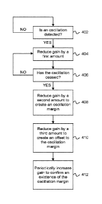
[0057] FIG 4 illustrates an exemplary technique for reducing oscillation in a
signal
booster. The technique can be implemented using a controller in the signal
booster. In
operation 402, the controller can determine whether an oscillation is
detected. If an
oscillation is not detected, then the controller can continue to check for
oscillations that
occur in the signal booster. If an oscillation is detected, then the
controller can reduce a
gain by a first amount, as in operation 404. In operation 406, the controller
can determine
whether the oscillation has ceased or stopped. If the oscillation has not
ceased or stopped,
then the controller can continue to reduce the gain until the oscillation has
ceased or
stopped. In operation 408, the controller can further reduce the gain by a
second amount
to create an oscillation margin. In operation 410, the controller can further
reduce the gain
by a third amount to create an offset to the oscillation margin. The first
amount, the
second amount and the third amount can be represented in decibels (dB). In
operation
412, the controller can periodically increase the gain to confirm an existence
of the
oscillation margin. In other words, the controller can periodically increase
the gain to
confirm an expected oscillation margin.
[0058] FIG 5 illustrates an exemplary technique for reducing oscillation in a
signal
booster. The technique can be implemented using a controller in the signal
booster. In
17
CA 03051248 2019-07-22
WO 2018/144639
PCT/US2018/016300
operation 502, the controller can determine whether an oscillation is
detected. If an
oscillation is not detected, then the controller can continue to check for
oscillations that
occur in the signal booster. If an oscillation is detected, then the
controller can reduce a
gain by a first amount, as in operation 504. In operation 506, the controller
can determine
whether the oscillation has substantially ceased or stopped. If the
oscillation has not
ceased or stopped, then the controller can continue to reduce the gain until
the oscillation
has ceased or stopped. The level at which the oscillation has substantially
ceased or
stopped is referred to as the oscillation threshold level. In operation 508,
the controller
can further reduce the gain from the oscillation threshold level by a second
amount to
create an oscillation margin. In operation 510, the controller can
periodically increase the
gain by a selected amount that is less than the second amount (the oscillation
margin) to
confirm an existence of the oscillation margin. When the controller increases
the gain by
the selected amount, it results in a capability to check the oscillation
margin, while
reducing a noise floor level of the signal booster relative to the signal
booster operating at
the oscillation threshold level. In addition, the technique illustrated in FIG
5 can enable
the signal booster to operate at a higher amplification level than when using
the technique
in FIG. 4, since there is no need to reduce the gain by the third amount.
[0059] FIG 6 provides an example illustration of the wireless device, such as
a user
equipment (UE), a mobile station (MS), a mobile communication device, a
tablet, a
handset, a wireless transceiver coupled to a processor, or other type of
wireless device.
The wireless device can include one or more antennas configured to communicate
with a
node or transmission station, such as an access point (AP), a base station
(BS), an evolved
Node B (eNB), a baseband unit (BBU), a remote radio head (RRH), a remote radio
equipment (RRE), a relay station (RS), a radio equipment (RE), a remote radio
unit
(RRU), a central processing module (CPM), or other type of wireless wide area
network
(WWAN) access point. The wireless device can communicate using separate
antennas for
each wireless communication standard or shared antennas for multiple wireless
communication standards. The wireless device can communicate in a wireless
local area
network (WLAN), a wireless personal area network (WPAN), and/or a WWAN.
[0060] FIG. 6 also provides an illustration of a microphone and one or more
speakers that
can be used for audio input and output from the wireless device. The display
screen can
be a liquid crystal display (LCD) screen, or other type of display screen such
as an
18
CA 03051248 2019-07-22
WO 2018/144639
PCT/US2018/016300
organic light emitting diode (OLED) display. The display screen can be
configured as a
touch screen. The touch screen can use capacitive, resistive, or another type
of touch
screen technology. An application processor and a graphics processor can be
coupled to
internal memory to provide processing and display capabilities. A non-volatile
memory
port can also be used to provide data input/output options to a user. The non-
volatile
memory port can also be used to expand the memory capabilities of the wireless
device.
A keyboard can be with the wireless device or wirelessly connected to the
wireless device
to provide additional user input. A virtual keyboard can also be provided
using the touch
screen.
Examples
[0061] The following examples pertain to specific technology embodiments and
point out
specific features, elements, or actions that can be used or otherwise combined
in
achieving such embodiments.
[0062] Example 1 includes a repeater, comprising: one or more amplification
and filtering
.. signal paths; and a controller configured to: detect an oscillation in the
repeater; reduce a
gain in the repeater by a first amount to cease the oscillation in the
repeater; reduce the
gain in the repeater further by a second amount to create an oscillation
margin; and
modify the gain in the repeater further by a third amount to create an offset
to the
oscillation margin.
[0063] Example 2 includes the repeater of Example 1, wherein the controller is
further
configured to periodically increase the gain in the repeater, wherein the
offset to the
oscillation margin reduces a likelihood that the increase to the gain causes a
subsequent
oscillation at the repeater.
[0064] Example 3 includes the repeater of any of Examples 1 to 2, wherein the
controller
is further configured to increase the gain by the oscillation margin.
[0065] Example 4 includes the repeater of any of Examples 1 to 3, wherein the
controller
is further configured to increase the gain by the offset to the oscillation
margin.
[0066] Example 5 includes the repeater of any of Examples 1 to 4, wherein the
controller
is further configured to increase the gain by the oscillation margin and the
offset to the
oscillation margin.
19
CA 03051248 2019-07-22
WO 2018/144639
PCT/US2018/016300
[0067] Example 6 includes the repeater of any of Examples 1 to 5, wherein the
controller
configured to modify the gain is configured to reduce the gain in the repeater
by the third
amount to create the offset to the oscillation margin.
[0068] Example 7 includes the repeater of any of Examples 1 to 6, wherein the
first
amount, the second amount and the third amount are represented in decibels
(dB).
[0069] Example 8 includes the repeater of any of Examples 1 to 7, wherein the
one or
more amplification and filtering signal paths include at least one of: one or
more uplink
amplification and filtering signal paths or one or more downlink amplification
and
filtering signal paths.
[0070] Example 9 includes the repeater of any of Examples 1 to 8, further
comprising: a
first antenna; and a second antenna.
[0071] Example 10 includes the repeater of any of Examples 1 to 9, further
comprising: a
first multi-band filter; and a second multi-band filter, wherein the first
multi-band filter is
communicatively coupled between the first antenna and the second antenna, and
the
second multi-band filter is communicatively coupled between the first antenna
and the
second antenna.
[0072] Example 11 includes the repeater of any of Examples 1 to 10, wherein
the
controller is further configured to perform network protection for the one or
more
amplification and filtering signal paths.
[0073] Example 12 includes a signal booster, comprising: one or more
amplification and
filtering signal paths; and a controller configured to: reduce a gain in the
signal booster by
a first amount to create an oscillation margin; and reduce the gain in the
signal booster
further by a second amount to create an additional margin to the oscillation
margin.
[0074] Example 13 includes the signal booster of Example 12, wherein the
controller is
configured to create the oscillation margin in response to detecting an
oscillation at the
signal booster.
[0075] Example 14 includes the signal booster of any of Examples 12 to 13,
wherein the
controller is further configured to periodically increase the gain in the
signal booster,
wherein the additional margin to the oscillation margin reduces a likelihood
that the
increase to the gain causes an oscillation at the signal booster.
CA 03051248 2019-07-22
WO 2018/144639
PCT/US2018/016300
[0076] Example 15 includes the signal booster of any of Examples 12 to 14,
wherein the
controller is further configured to increase the gain by the oscillation
margin.
[0077] Example 16 includes the signal booster of any of Examples 12 to 15,
wherein the
controller is further configured to increase the gain by the offset to the
oscillation margin.
[0078] Example 17 includes the signal booster of any of Examples 12 to 16,
wherein the
controller is further configured to increase the gain by the oscillation
margin and the
offset to the oscillation margin.
[0079] Example 18 includes the signal booster of any of Examples 12 to 17,
wherein the
first amount and the second amount are represented in decibels (dB).
[0080] Example 19 includes at least one non-transitory machine readable
storage medium
having instructions embodied thereon for reducing oscillation in a signal
booster, the
instructions when executed by one or more processors perform the following:
determining an oscillation amplification threshold level at which oscillation
is
substantially reduced or ceases to occur at the signal booster; selecting an
oscillation
margin level; operating the signal booster at an amplification level that is
the oscillation
margin level below the oscillation amplification threshold level; selecting an
oscillation
margin offset level that is less than the oscillation margin level; increasing
a gain of the
signal booster by the oscillation margin offset level to periodically
determine if an
oscillation occurs at the signal booster while operating at the increased gain
level,
wherein the oscillation margin offset level for the increased gain reduces a
noise floor
impact of the signal booster; and decreasing the gain of the signal booster by
the
oscillation margin offset level to operate the signal booster at the
amplification level.
[0081] Example 20 includes the at one non-transitory machine readable storage
medium
of Example 19, further comprising instructions when executed perform the
following:
amplifying and filtering signals in at least one of an uplink or a downlink.
[0082] Example 21 includes the at one non-transitory machine readable storage
medium
of any of Examples 19 to 20, further comprising instructions when executed
perform the
following: selecting the oscillation margin offset level to reduce a
transmitted noise
power from the signal booster.
[0083] Example 22 includes the at one non-transitory machine readable storage
medium
21
CA 03051248 2019-07-22
WO 2018/144639
PCT/US2018/016300
of any of Examples 19 to 21, wherein the oscillation margin offset level and
the
oscillation margin level are represented in decibels (dB).
[0084] Various techniques, or certain aspects or portions thereof, can take
the form of
program code (i.e., instructions) embodied in tangible media, such as floppy
diskettes,
compact disc-read-only memory (CD-ROMs), hard drives, non-transitory computer
readable storage medium, or any other machine-readable storage medium wherein,
when
the program code is loaded into and executed by a machine, such as a computer,
the
machine becomes an apparatus for practicing the various techniques. Circuitry
can
include hardware, firmware, program code, executable code, computer
instructions,
and/or software. A non-transitory computer readable storage medium can be a
computer
readable storage medium that does not include signal. In the case of program
code
execution on programmable computers, the computing device can include a
processor, a
storage medium readable by the processor (including volatile and non-volatile
memory
and/or storage elements), at least one input device, and at least one output
device. The
volatile and non-volatile memory and/or storage elements can be a random-
access
memory (RAM), erasable programmable read only memory (EPROM), flash drive,
optical drive, magnetic hard drive, solid state drive, or other medium for
storing
electronic data. One or more programs that can implement or utilize the
various
techniques described herein can use an application programming interface
(API), reusable
controls, and the like. Such programs can be implemented in a high level
procedural or
object oriented programming language to communicate with a computer system.
However, the program(s) can be implemented in assembly or machine language, if
desired. In any case, the language can be a compiled or interpreted language,
and
combined with hardware implementations.
[0085] As used herein, the term processor can include general purpose
processors,
specialized processors such as VLSI, FPGAs, or other types of specialized
processors, as
well as base band processors used in transceivers to send, receive, and
process wireless
communications.
[0086] It should be understood that many of the functional units described in
this
specification have been labeled as modules, in order to more particularly
emphasize their
implementation independence. For example, a module can be implemented as a
hardware
22
CA 03051248 2019-07-22
WO 2018/144639
PCT/US2018/016300
circuit comprising custom very-large-scale integration (VLSI) circuits or gate
arrays, off-
the-shelf semiconductors such as logic chips, transistors, or other discrete
components. A
module can also be implemented in programmable hardware devices such as field
programmable gate arrays, programmable array logic, programmable logic devices
or the
like.
[0087] In one example, multiple hardware circuits or multiple processors can
be used to
implement the functional units described in this specification. For example, a
first
hardware circuit or a first processor can be used to perform processing
operations and a
second hardware circuit or a second processor (e.g., a transceiver or a
baseband
processor) can be used to communicate with other entities. The first hardware
circuit and
the second hardware circuit can be incorporated into a single hardware
circuit, or
alternatively, the first hardware circuit and the second hardware circuit can
be separate
hardware circuits.
[0088] Modules can also be implemented in software for execution by various
types of
processors. An identified module of executable code can, for instance,
comprise one or
more physical or logical blocks of computer instructions, which can, for
instance, be
organized as an object, procedure, or function. Nevertheless, the executables
of an
identified module need not be physically located together, but can comprise
disparate
instructions stored in different locations which, when joined logically
together, comprise
the module and achieve the stated purpose for the module.
[0089] Indeed, a module of executable code can be a single instruction, or
many
instructions, and can even be distributed over several different code
segments, among
different programs, and across several memory devices. Similarly, operational
data can
be identified and illustrated herein within modules, and can be embodied in
any suitable
form and organized within any suitable type of data structure. The operational
data can
be collected as a single data set, or can be distributed over different
locations including
over different storage devices, and can exist, at least partially, merely as
electronic signals
on a system or network. The modules can be passive or active, including agents
operable
to perform desired functions.
[0090] Reference throughout this specification to "an example" or "exemplary"
means
that a particular feature, structure, or characteristic described in
connection with the
23
CA 03051248 2019-07-22
WO 2018/144639
PCT/US2018/016300
example is included in at least one embodiment of the present invention. Thus,
appearances of the phrases "in an example" or the word "exemplary" in various
places
throughout this specification are not necessarily all referring to the same
embodiment.
[0091] As used herein, a plurality of items, structural elements,
compositional elements,
and/or materials can be presented in a common list for convenience. However,
these lists
should be construed as though each member of the list is individually
identified as a
separate and unique member. Thus, no individual member of such list should be
construed as a de facto equivalent of any other member of the same list solely
based on
their presentation in a common group without indications to the contrary. In
addition,
various embodiments and example of the present invention can be referred to
herein
along with alternatives for the various components thereof It is understood
that such
embodiments, examples, and alternatives are not to be construed as defacto
equivalents of
one another, but are to be considered as separate and autonomous
representations of the
present invention.
[0092] Furthermore, the described features, structures, or characteristics can
be combined
in any suitable manner in one or more embodiments. In the following
description,
numerous specific details are provided, such as examples of layouts,
distances, network
examples, etc., to provide a thorough understanding of embodiments of the
invention.
One skilled in the relevant art will recognize, however, that the invention
can be practiced
without one or more of the specific details, or with other methods,
components, layouts,
etc. In other instances, well-known structures, materials, or operations are
not shown or
described in detail to avoid obscuring aspects of the invention.
[0093] While the forgoing examples are illustrative of the principles of the
present
invention in one or more particular applications, it will be apparent to those
of ordinary
skill in the art that numerous modifications in form, usage and details of
implementation
can be made without the exercise of inventive faculty, and without departing
from the
principles and concepts of the invention. Accordingly, it is not intended that
the invention
be limited, except as by the claims set forth below.
24